

Cherry Semiconductor CS5101EN14, CS5101EDWR16, CS5101EDW16 Datasheet
1
Features
■
1.5A Peak Output
(Grounded Totem Pole)
■
8V to 75V Gate Drive Voltage
■
8V to 45V Supply Voltage
■
300ns Propagation Delay
■
1% Error Amplifier
Reference Voltage
■
Lossless Turn On and
Turn Off
■
Sleep Mode: < 100µA
■
Overcurrent Protection with
Dedicated Differential Amp
■
Synchronization to External
Clock
■
External Power Switch
Drain Voltage Monitor
Package Options
16L SO Wide
14L PDIP
CS5101
Secondary Side Post Regulator for AC/DC
and DC/DC Multiple Output Converters
SYNC
V
CC
V
REF
DGnd
V
FB
COMP
RAMP
V
C
PGnd
IS-
IS+
IS COMP
V
D
V
G
PGnd
AGnd
SYNC
V
CC
V
REF
LGnd
V
FB
COMP
RAMP
V
C
PGnd
IS-
IS+
IS COMP
V
D
V
G
CS5101
Description
The CS5101 is a bipolar monolithic
secondary side post regulator
(SSPR) which provides tight regulation of multiple output voltages in
AC-DC or DC-DC converters.
Leading edge pulse width modulation is used with the CS5101.
The CS5101 is designed to operate
over an 8V to 45V supply voltage
(VCC) range and up to a 75V drive
voltage (VC).
The CS5101 features include a totem
pole output with 1.5A peak output
current capability, externally programmable overcurrent protection,
an on chip 2% precision 5V reference, internally compensated error
amplifier, externally synchronized
switching frequency, and a power
switch drain voltage monitor. It is
available in a 14 lead plastic DIP or
a 16 lead wide body SO package.
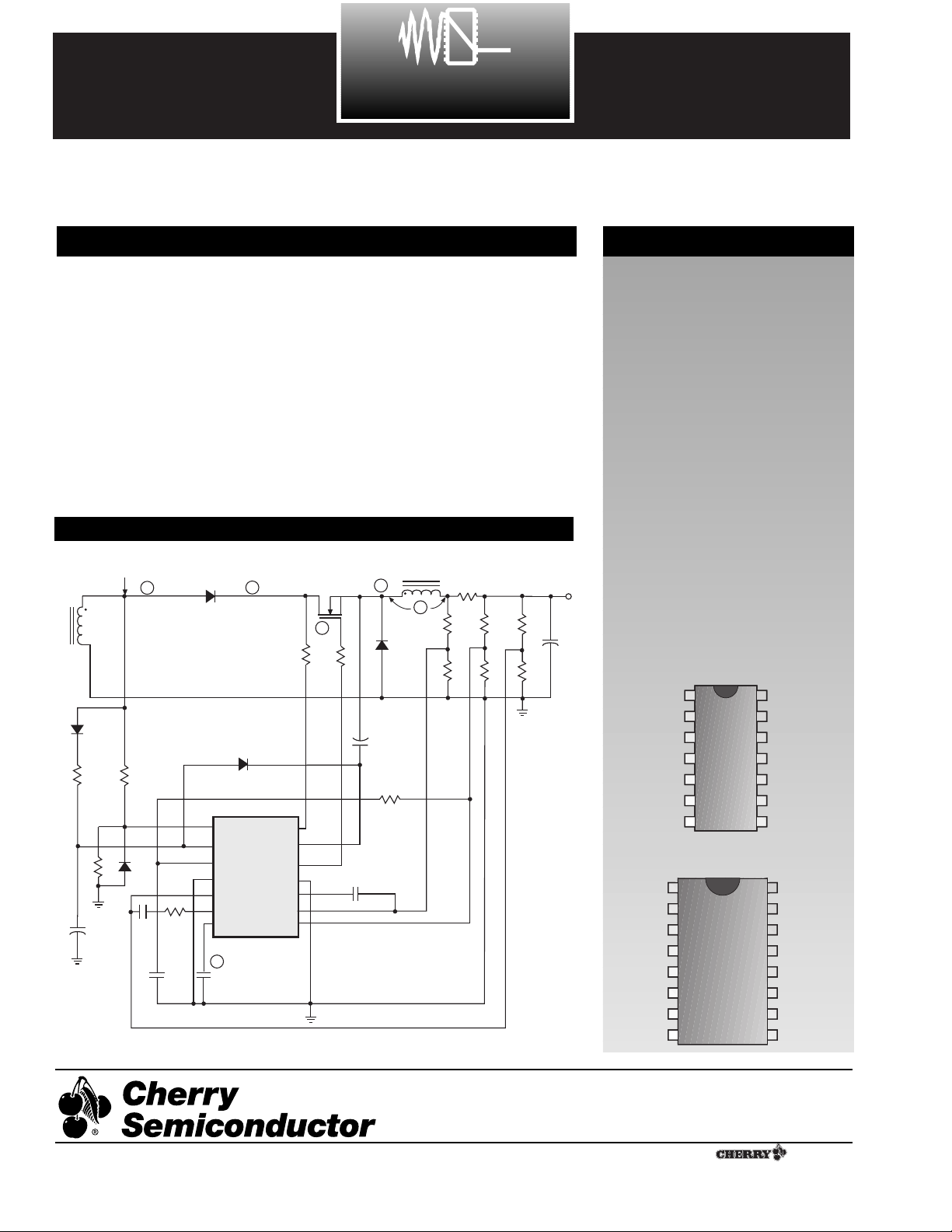
Application Diagram
Cherry Semiconductor Corporation
2000 South County Trail, East Greenwich, RI 02818
Tel: (401)885-3600 Fax: (401)885-5786
Email: info@cherry-semi.com
Web Site: www.cherry-semi.com
A Company
¨
Rev. 3/31/97
V
SY
TR
C
R1
1
C
R4
3
L1
Q1
6
R5
4
C
R6
R5
C5
+
R10
5
R8
R11
R12
R9
R14
R13
Gnd
V
OUT
+
C6
1
R1
+
R2
C
R3
R2
R4
C1
C2
C3
V
V
V
LGnd
V
COMP
RAMP
2
C
SYNC
CC
REF
FB
R
C
R3
CS5101
SSPR
PGnd
IS COMP
R7
V
D
V
C
V
G
C4
IS-
IS+
1

2
PARAMETER TEST CONDITIONS MIN TYP MAX UNIT
CS5101
Absolute Maximum Ratings
Power Supply Voltage, VCC.....................................................................................................................................-0.3V to 45V
V
SYNC
and Output Supply Voltages, VC, VG, V
SYNC
, VD.....................................................................................-0.3V to 75V
VIS+, VIS- (VCCÐ 4V, up to 24V)..................................................................................................................................-0.3 to 24V
V
REF
, VFB, V
COMP
, V
RAMP
, V
ISCOMP
............................................................................................................................-0.3 to 10V
Operating Junction Temperature, TJ.......................................................................................................................-40 to 150¡C
Operating Temperature Range ..................................................................................................................................-40 to 85¡C
Storage Temperature Range ....................................................................................................................................-65 to 150¡C
Output Energy (capacitive load per cycle).............................................................................................................................5µJ
ESD Human Body ....................................................................................................................................................................2kV
ESD Machine Model...............................................................................................................................................................200V
Lead Temperature Soldering
Wave Solder (through hole styles only)....................................................................................10 sec. max, 260¡C peak
Reflow (SMD styles only).....................................................................................60 sec. max above 183¡C, 230¡C peak
Electrical Characteristics:
-40¡C ² TA² 85¡C; -40¡C ² TJ² 150¡C; 10V < VCC< 45V; 8V < VC<75V unless otherwise specified.
■ Error Amplifier
Input Voltage Initial Accuracy V
FB
= V
COMP
; VCC= 15V; 1.98 2.00 2.02 V
T = 25¡C (Note 1)
Input Voltage V
FB
= V
COMP
, includes line and temp 1.94 2.00 2.06 V
Input Bias Current V
FB
= 0V; IVFBflows out of pin 500 nA
Open Loop Gain 1.5V < V
COMP
< 3.0V 60 70 dB
Unity Gain Bandwidth 1.5V < V
COMP
< 3.0V; (Note 1) 0.7 1.0 MHz
Output Sink Current V
COMP
= 2.0V; VFB= 2.2V 2 8 mA
Output Source Current V
COMP
= 2.0V; VFB= 1.8V 2 6 mA
V
COMP
High VFB= 1.8V 3.3 3.5 3.7 V
V
COMP
Low VFB= 2.2V 0.85 1.0 1.15 V
PSRR 10V < V
CC
< 45V; 60 70 dB
V
FB
= V
COMP
(Note 1)
■ Voltage Reference
Output Voltage Initial Accuracy V
CC
= 15V; T = 25¡C (Note 1) 4.9 5.0 5.1 V
Output Voltage 0A < I
REF
< 8mA 4.8 5.0 5.2 V
Line Regulation 10V < V
CC
< 45V; I
REF
= 0A 10 60 mV
Load Regulation 0A < I
REF
< 8mA 20 60 mV
Current Limit V
REF
= 4.8V 10 50 mA
V
REF
_OK FAULT V V
SYNC
= 5V; V
REF
= V
LOAD
4.10 4.40 4.60 V
V
REF
_OK V V
SYNC
= 5V; V
REF
= V
LOAD
4.30 4.50 4.80 V
V
REF
_OK Hysteresis 40 100 250 mV
■ Current Sense Amplifier
IS COMP High V IS
+
= 5V; ISÐ= IS COMP 4.7 5.0 5.3 V
IS COMP Low V IS
+
= 0V; ISÐ= IS COMP 0.5 1.0 1.3 V
Source Current IS
+
= 5V; ISÐ= 0V 2.0 10 mA
Sink Current IS
-
= 5V; IS+= 0V 10 20 mA
Open Loop Gain 1.5V ² V
COMP
² 4.5V; RL= 4k½ 60 80 dB
CMRR (Note 1) 60 80 dB
PSRR 10V < V
CC
< 45V, (Note 1) 60 80 dB
Unity Gain Bandwidth 1.5V ² V
COMP
² 4.5V; RL= 4k½ (Note 1) 0.5 0.8 MHz

3
CS5101
Electrical Characteristics: continued
PARAMETER TEST CONDITIONS MIN TYP MAX UNIT
■ Current Sense Amplifier: continued
Input Offset Voltage V
IS
+ = 2.5V; VIS- = V
ISCOMP
-8 0 8 mV
Input Bias Currents V
IS
+ = VIS- = 0V; IISflows out of pins 20 250 nA
Input Offset Current (IS
+
, IS-) -250 0 250 nA
Input Signal Voltage Range (Note 1) -0.3 V
CC
-4.0 V
■ RAMP/SYNC Generator
Ramp Source Current Initial V
SYNC
= 5V, V
RAMP
= 2.5V ; T = 25¡C 0.18 0.20 0.22 mA
Accuracy (Note 1)
Ramp Source Current V
SYNC
= 5V; V
RAMP
= 2.5V 0.16 0.20 0.24 mA
Ramp Sink Current V
SYNC
= 0V; V
RAMP
= 2.5V 1.0 4.0 mA
RAMP Peak Voltage V
SYNC
= 5V 3.3 3.5 3.7 V
RAMP Valley Voltage V
SYNC
= 0V 1.4 1.5 1.6 V
RAMP Dynamic Range V
RAMPDR
= V
RAMPPK
Ð V
RAMPVY
1.7 2.0 2.3 V
RAMP Sleep Threshold Voltage V
RAMP
@ V
REF
< 2.0V 0.3 0.6 1.0 V
SYNC Threshold V
SYNC
@ V
RAMP
> 2.5V 2.3 2.5 2.7 V
SYNC Input Bias Current V
SYNC
= 0V; I
SYNC
flows out of pin 1 20 µA
■ Output Stage
V
G
, High V
SYNC
= 5V; IVG= 200mA, VCÐ V
G
1.6 2.5 V
V
G
, Low V
SYNC
= 0V; IVG= 200mA 0.9 1.5 V
V
G
Rise Time Switch V
SYNC
High; CG= 1nF; 30 75 ns
VCC= 15V; measure 2V to 8V
V
G
Fall Time Switch V
SYNC
Low; CG= 1nF 40 100 ns
VCC= 15V; measure 8V to 2V
V
G
Resistance to Gnd Remove supplies; VG= 10V 50 100 k½
V
D
Resistance to Gnd Remove supplies; VD= 10V 500 1500 ½
■ General
I
CC
, Operating V
SYNC
= 5V 12 18 mA
I
CC
in UVL VCC= 6V 300 500 µA
I
CC
in Sleep Mode High V
RAMP
= 0V; VCC= 45V 80 200 µA
I
CC
In Sleep Mode Low V
RAMP
= 0V; VCC= 10V 20 50 µA
I
C
, Operating High V
SYNC
= 5V; V
FB
= VISÐ = 0V; 4 8 mA
VC= 75V
I
C
, Operating Low V
SYNC
= 5V; V
FB
= VISÐ = 0V; VC= 8V 3 6 mA
UVLO Start Voltage 7.4 8.0 9.2 V
UVLO Stop Voltage 6.4 7.0 8.3 V
UVLO Hysteresis 0.8 1.0 1.2 V
Leading Edge, t
DELAY
V
SYNC
= 2.5V to VG= 8V 280 ns
Trailing Edge, t
DELAY
V
SYNC
= 2.5V to VG= 2V 750 ns
Note 1: Guaranteed by design. Not 100% tested in production.
 Loading...