

Cherry Semiconductor CS453GTVA5, CS453GTHA5, CS453GT5, CS452GTVA5, CS452GTHA5 Datasheet
...
1
Features
■
Microprocessor
Compatible Inputs
■ On-Chip Power Device
2.4A Peak, Typical CS-452
4.4A Peak, Typical CS453
■ Low Thermal Resistance
To Grounded Tab
■ 60V Peak Transient
Voltage
■ Low Saturation Voltage
■ Operates Over a 4.5V to
24V Battery Range
Package Options
5 Lead TO-220
Tab (Gnd)
1
CS452/453
2.4A/4.4A Injector Solenoid Driver
CS452/453
Description
The CS452/453 is a monolithic integrated circuit designed for medium
current solenoid driver applications. Its typical function is to supply full battery voltage to fuel injector(s) for rapid current rise, in order
to produce positive injector opening.
When load current reaches a preset
level (2.4A for CS452, or 4.4A for
CS453), the injector driver reduces
the load current by a 4:1 ratio and
operates as a constant current
source. This condition holds the
injector open and reduces system
power dissipation.
Other solenoid or relay applications
can be equally well served by the
CS452/453. Two high impedance
inputs are provided which permit a
variety of control options and can
be driven by TTL or CMOS logic.
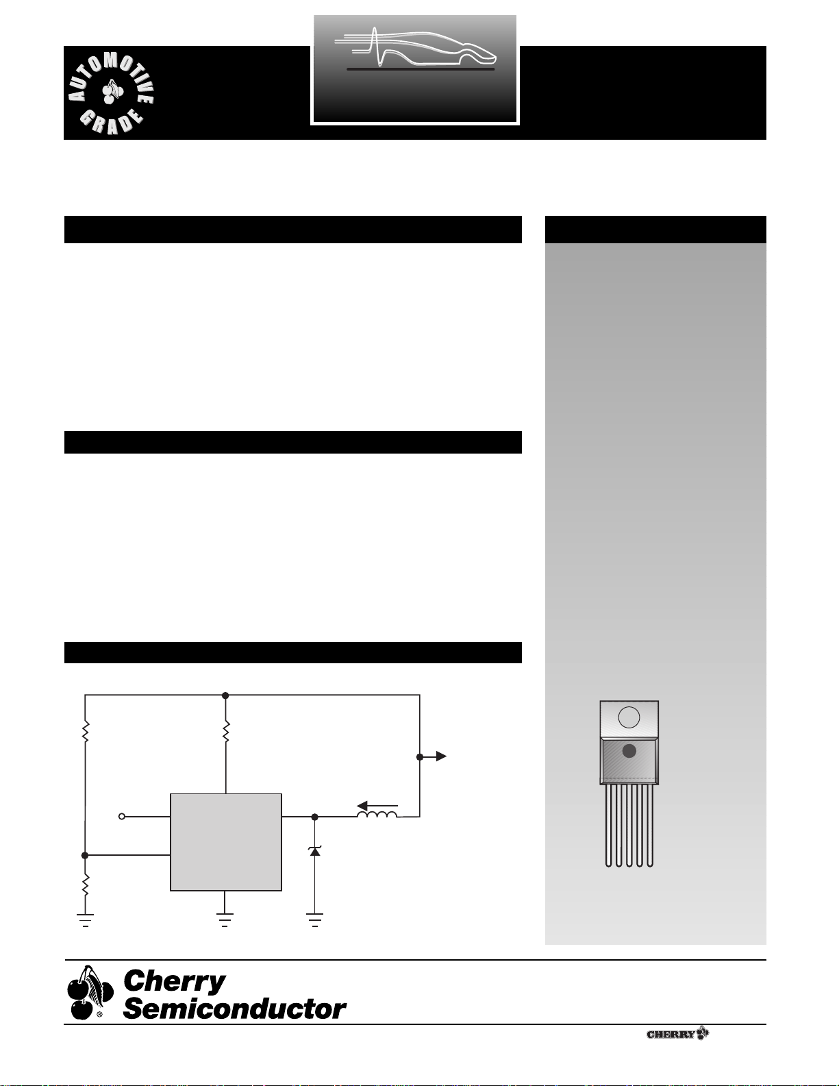
Typical Application Diagram
Absolute Maximum Ratings
Power Supply Voltage (VCC) .........................................................................24V
VIN..........................................................................................................-6.0 to 24V
Control ..................................................................................................-6.0 to 24V
Peak Transient Voltage (46V Load Dump)..................................................60V
Internal Regulator Current.........................................................................50mA
Junction Temperature Range....................................................-40¡C to +150¡C
Operating Temperature Range (Tab Temperature) ..............-40¡C to +125¡C
Storage Temperature Range .....................................................-65¡C to +150¡C
Lead Temperature Soldering
Wave Solder (through hole styles only)...10 sec. max, 260¡C peak
1V
IN
2 CONTROL
3 Gnd
4 OUT
5V
CC
Cherry Semiconductor Corporation
2000 South County Trail, East Greenwich, RI 02818
Tel: (401)885-3600 Fax: (401)885-5786
Email: info@cherry-semi.com
Web Site: www.cherry-semi.com
A Company
¨
Rev. 12/18/97
19kW
V
IN
V
IN
CONTROL
300W
V
CC
CS452/453
I
OUT
OUT
Injector
40VZ (max)
V
BAT
4.5V to 24V
(60V Transient)
1kW
Gnd
2
PACKAGE LEAD # LEAD SYMBOL FUNCTION
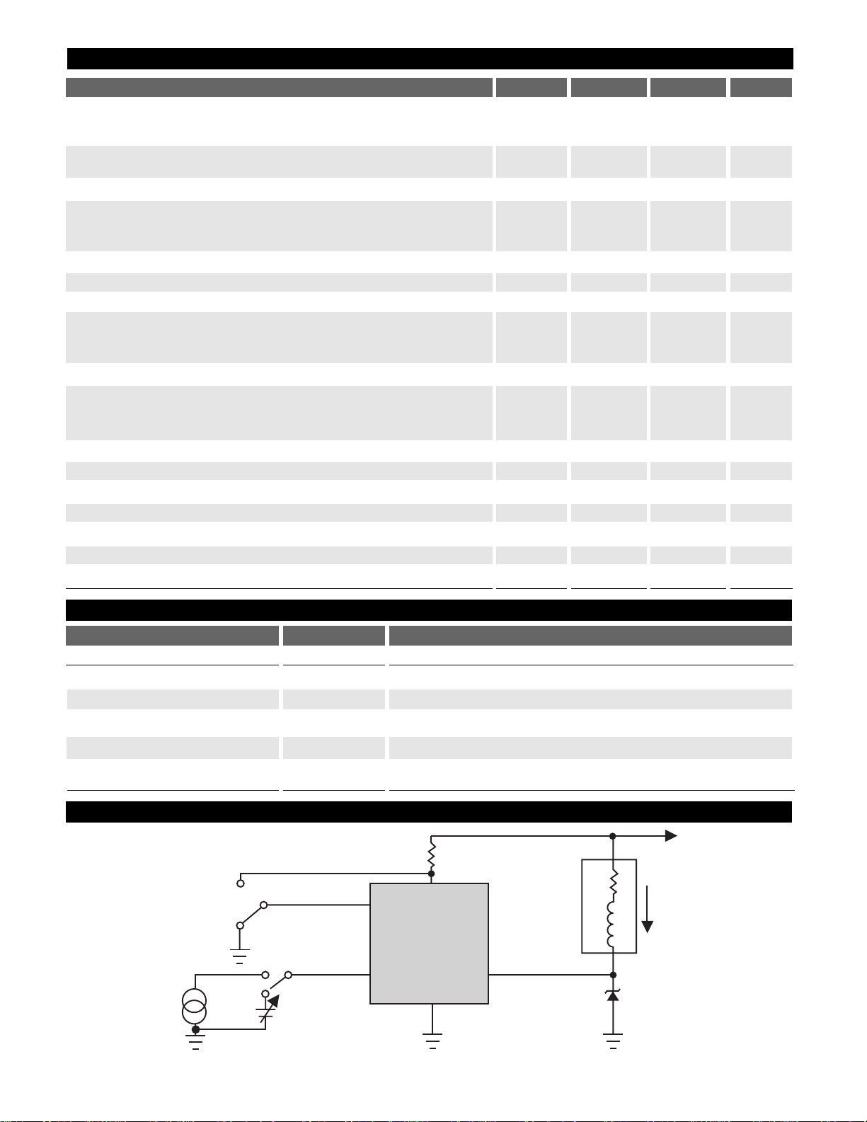
Electrical Characteristics:
V
BAT
= 12 VDC, TA= 25ûC, test circuit of Test Circuit diagram, unless noted
CHARACTERISTIC MIN TYP MAX UNIT
CS452/453
Test Circuit
Package Lead Description
Output Peak Current (Ipk) CS452 1.7 2.4 2.9 A
CS453 3.6 4.4 5.2 A
Output Sustaining Current (I
sus
) CS452 0.50 0.60 0.70 A
CS453 0.95 1.12 1.25 A
V
(BR)CEO(sus)
@ 1mA 42 50 V
Output Voltage in Saturated Mode
CS452 @ 1.5A 1.2 V
CS453 @ 3.0A 1.6 V
Internal Regulated Voltage (@V
CC
, Test Circuit diagram) 6.9 V
Input ÒonÓ Threshold Voltage 1.4 2.0 V
Input ÒoffÓ Threshold Voltage 0.7 1.3 V
Input ÒonÓ Current
@ V
IN
= 1.4V
DC
35 µA
@ V
IN
= 5.0V
DC
220 µA
CONTROL ÒonÓ Threshold Voltage 1.2 1.5 1.8 V
CONTROL Current
CONTROL = 0.8V
DC
-5 -50 µA
CONTROL = 5.0V
DC
1.0 µA
Input Turn On Delay (t
l
) 0.5 1.0 µs
I
pk
sense to I
sus
delay (tp)60µs
CONTROL Signal Delay (t
t
)15µs
Input Turn Off from Saturated Mode Delay (t
s
) 1.0 µs
Input Turn Off from Sustain Mode Delay (t
d
) 0.2 µs
Output Voltage Rise Time (t
v
) 0.4 µs
Output Current Fall Time (t
f
) 4.0A 0.6 1.0 µs
TO-220
1V
IN
Switches the injector driver on and off.
2 CONTROL Acts to disable OUT when high.
3 Gnd Ground connection.
4 OUT Output Drive current.
5V
CC
Supply voltage to IC. VCCis connected to V
BAT
through a series
resistor (300½ typ.)
300 W/2W
1.2
2.0
mH
5 V
p-p
250Hz
Square
Wave
High
Low
S2
S1
0-5.0 V
DC
CONTROL
CS452/453
V
IN
V
CC
Gnd
OUT
R
L
40 V/10 W
Zener
V
BAT
Injector
Load
I
 Loading...