

Cherry Semiconductor CS4172XN16, CS4172XDWFR16, CS4172XDWF16 Datasheet
1
Features
■ Serial Input Bus
■ 2 MHz Operating
Frequency
■ Tangential Drive
Algorithm
■ 80mA Drive Circuits
■ 0.5¡ Accuracy (Typ.)
■ Power-On-Reset
■ Protection Features
Output Short Circuit
Overtemperature
Package Options
Single Air-Core Gauge Driver
CS4172
Description
The CS4172 is a monolithic BiCMOS
integrated circuit used to translate a
digital 10-bit word from a microprocessor/microcontroller to complementary DC outputs. The DC outputs
drive an air-core meter commonly
used in vehicle instrument panels. The
10 bits of data are used to linearly control the quadrature coils of the meter
directly with a 0.35¡ resolution and
±1.0¡ accuracy over the full 360¡ range
of the gauge. The interface from the
microcontroller is by a Serial Peripheral Interface (SPI) compatible serial
connection using up to a 2MHz shift
clock rate.
The digital code, which is directly proportional to the desired gauge pointer
deflection, is shifted into a DAC and
multiplexer. These two blocks provide
a tangential conversion function to
change the digital data into the appropriate DC coil voltage for the angle
demanded. The tangential algorithm
creates approximately 40% more
torque in the meter movement than
does a sin-cos algorithm at 45¡, 135¡,
225¡, and 315¡ angles. This increased
torque reduces the error due to pointer
droop at these critical angles.
Each output buffer is capable of supplying up to 80mA per coil and are
controlled by a common enable pin.
When OE is low the output buffers are
turned off but the logic portion of the
chip remains powered and continues
to operate normally.
The Serial Gauge Driver is self-protected against output short circuit conditions. The output drivers are disabled
anytime the on-chip protection circuitry detects a short circuit condition. The
outputs remain off until a falling edge
is presented on CS. If the short circuit
is still present the output drivers automatically disable themselves again. A
thermal protection circuit limits the
junction temperature to approximately
160¡C for conditions of high supply
voltage and high ambient temperature.
The status pin (ST) reflects the state of
the outputs and is low whenever the
outputs are disabled.
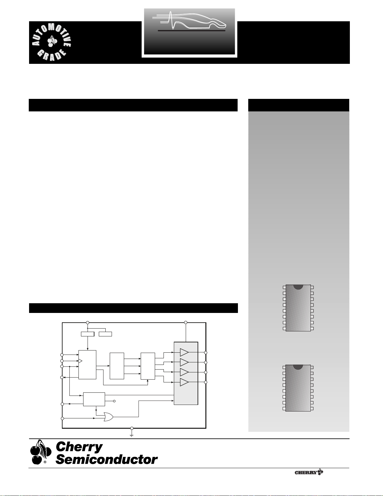
Block Diagram
16 Lead PDIP
SIN
-
SIN
+
Gnd
V
BB
Gnd
NC
SO
SI
V
CC
COS
+
COS
-
CS
SCLK
OE
Gnd
ST
SIN
-
SIN
+
Gnd
V
BB
Gnd
Gnd
SO
SI
V
CC
COS
+
COS
-
CS
SCLK
OE
1
Gnd
ST
16 Lead SO Wide
(internally fused leads)
Rev. 4/19/99
CS4172
Cherry Semiconductor Corporation
2000 South County Trail, East Greenwich, RI 02818
Tel: (401)885-3600 Fax: (401)885-5786
Email: info@cherry-semi.com
Web Site: www.cherry-semi.com
A Company
¨
V
POR
CC
LOGIC
V
BB
1
+
SI
SCLK
CS
SO
ST
OE
Serial
to
D0 Ð D6
Parallel
Shift
Register
D7 Ð D9
RS
FAULT
Latch
S
7 Bit
DAC
POR
Gnd
V
TOP
MUX
V
VAR
V
BAT
OC
Output
Amplifiers
SIN
SIN
COS
COS
Ð
+
Ð
2
Absolute Maximum Ratings
Supply Voltage
V
BB
....................................................................................................................................................................-1.0V to 15.0V
VCC......................................................................................................................................................................-1.0V to 6.0V
Digital Inputs ..............................................................................................................................................................-1.0V to 6.0V
Ground Potential Difference (|AGnd-DGnd|)....................................................................................................................0.5V
Steady State Output Current ............................................................................................................................................±100mA
Forced Injection Current (Inputs and Supply).................................................................................................................±10mA
Operating Junction Temperature (TJ) ..................................................................................................................................150¡C
Storage Temperature Range .................................................................................................................................-65¡C to 150¡C
Lead Temperature Soldering
Wave Solder (through hole styles only) .....................................................................................10 sec. max, 260¡C peak
Reflow (SMD styles only) ......................................................................................60 sec. max above 183¡C, 230¡C peak
ESD Susceptibility (Human Body Model)..............................................................................................................................2kV
CS4172
Electrical Characteristics: -40¡C ² TA² 105¡C; 7.5V ² VBB² 14V; 4.5V ² VCC² 5.5V (unless otherwise specified)
PARAMETER TEST CONDITIONS MIN TYP MAX UNIT
■ Supply Voltages and Currents
VBBQuiescent Current Output disabled (OE = 0V) 1 5 mA
[R
COS
, R
SIN
= R
L(MIN)
] @45¡ 175 mA
(code = XÕ080) VBB= 14V
VCCQuiescent Current OE = high, V
BB
= 0V
SCLK = 2.0MHz 1 mA
■ Digital Inputs and Outputs
Output High Voltage SO, I
OH
= 0.8mA V
CC
- 0.8 V
Output Low Voltage SO, I
OL
=0.8mA 0.4 V
ST, I
OL
= 2.5mA 0.8 V
Output High Current ST, V
CC
= 5.0V 25 µA
Input High Voltage CS, SCLK, SI, OE 0.7 ´ V
CC
V
Input Low Voltage CS, SCLK, SI, OE 0.3 ´ V
CC
V
Input High Current CS, SCLK, SI, OE; V
IN
= 0.7 ´ V
CC
1µA
Input Low Current CS, SCLK, SI, OE; V
IN
= 0.3 ´ V
CC
1µA
■ Analog Outputs
Output Function Accuracy -1.2 +1.2 deg
Output Shutdown Current, V
BB
= 14.0V 70 250 mA
Source
Output Shutdown Current, V
BB
= 14.0V 70 250 mA
Sink
Output Shutdown Current, V
BB
= 7.5V 43 250 mA
Source
Output Shutdown Current, V
BB
= 7.5V 43 250 mA
Sink
Coil Drive Output Voltage 0.748 ´ V
BB
V
Minimum Load Resistance TA= 105¡C 229 ½
TA= 25¡C 171 ½
TA= -40¡C 150 ½
 Loading...