

Cherry Semiconductor CS4124YN16 Datasheet
Features
■ 150mA Peak PWM Gate
Drive Output
■ Patented Voltage
Compensation Circuit
■ 100% Duty Cycle
Capability
■ 5V, ± 3% Linear Regulator
■ Low Current Sleep Mode
■ Overvoltage Protection
■ Boost Mode Power
Supply
■ Output Inhibit
Package Option
CS4124
High Side PWM FET Controller
CS4124
Description
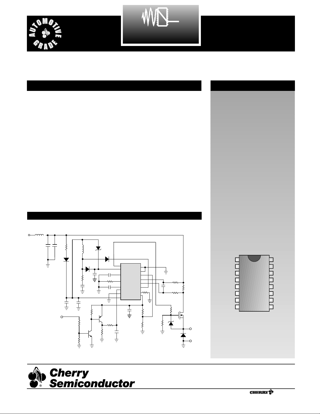
Applications Diagram
Preliminary
OUTPUT
Gnd
INH
I
ADJ
PMP
SNI
V
REG
BOOST
FLT
R
OSC
C
OSC
CTL
PGnd
V
CC
I
SENSE+
I
SENSE-
16 Lead PDIP
1195
Consult Factory for 16 Lead SOIC
Wide package.
Rev. 4/26/99
Cherry Semiconductor Corporation
2000 South County Trail, East Greenwich, RI 02818
Tel: (401)885-3600 Fax: (401)885-5786
Email: info@cherry-semi.com
Web Site: www.cherry-semi.com
A Company
®
The CS4124 is a monolithic integrated circuit designed primarily to
control the rotor speed of permanent magnet, direct current (DC)
brush motors. It drives the gate of
an N channel power MOSFET or
IGBT with a user-adjustable, fixed
frequency, variable duty cycle,
pulse width modulated (PWM) signal. The CS4124 can also be used to
control other loads such as incandescent bulbs and solenoids.
Inductive current from the motor or
solenoid is recirculated through an
external diode.
The CS4124 accepts a DC level
input signal of 0 to 5V to control the
pulse width of the output signal.
This signal can be generated by a
potentiometer referenced to the onchip 5V linear regulator, or a filtered 0% to 100% PWM signal also
referenced to the 5V regulator.
The IC is placed in a sleep state by
pulling the CTL lead below 0.5V. In
this mode everything on the chip is
shutdown except for the on-chip
regulator and the overall current
draw is less than 275µA. There are a
number of on-chip diagnostics that
look for potential failure modes and
can disable the external power
MOSFET.
V
BAT
42.5µH
1000µF
1000µF
10K
10nF
100µF
.01µF
C
FLT
.25µF
R
OSC
C
OSC
470pF
93.1K
OUTPUT
Gnd
INH
BOOST
FLT
R
OSC
I
ADJ
PMP
SNI
V
REG
C
OSC
CTL
PGnd
V
CC
P1
N1
10µF
10K
100K
10K
10K
10K
R
CS1
51
R
CS2
51
C
CS
.022µF
10K
10K
Input
470µH
MOT+
R
GATE
6
R
SENSE
4m
R
SNI
4
1.5µF
1µF
1M
I
SENSE+
I
SENSE-
MOT-
R
S
10
1
Electrical Characteristics:
4V ≤ VCC≤ 26V, -40˚C < TA< 125°C, (unless otherwise specified)
CS4124
1196
Absolute Maximum Ratings
Storage Temperature ................................................................................................................................................-65˚C to 150˚C
V
CC
.................................................................................................................................................................................-0.3V to 30V
V
CC
Peak Transient Voltage (load dump = 26V w/series 10Ω resistor) ...........................................................................40V
Input Voltage Range (at any input) ...........................................................................................................................-0.3V to 10V
Maximum Junction Temperature ..........................................................................................................................................150˚C
Lead Temperature Soldering
Wave Solder (through hole styles only) ......................................................................................10 sec. max, 260°C peak
ESD Capability (Human Body Model) ....................................................................................................................................2kV
PARAMETER TEST CONDITIONS MIN TYP MAX UNIT
■ V
CC
Supply
Operating Current Supply 7V ≤ VCC≤ 18V 5 10 mA
4V ≤ VCC< 7V, 18V < VCC≤ 26V 15 mA
Quiescent Current VCC= 12V 170 275 µA
Overvoltage Shutdown 26.5 29 V
■ Control (CTL)
Control Input Current CTL = 0V to 5V -2 0.1 2 µA
Sleep Mode Threshold 8% 10% 12% V
REG
Sleep Mode Hysteresis 7V ≤ VCC≤ 26V 50 100 150 mV
4V ≤ VCC< 7V 10 150 mV
■ Current Sense
Differential Voltage Sense 7V ≤ VCC≤ 18V
I
ADJ
= 1V and R
CS1
= 51Ω 18 34 mV
I
ADJ
= 4V and R
CS1
= 51Ω 104 125 mV
4V ≤ VCC< 7V
I
ADJ
=1V and R
CS1
= 51Ω 15 39 mV
18V < VCC≤ 26V
I
ADJ
= 1V and R
CS1
= 51Ω 15 39 mV
I
ADJ
= 4V and R
CS1
= 51Ω 102 130 mV
I
ADJ
Input Current 4V ≤ VCC≤ 26V -2 0.3 2 µA
I
ADJ
= 0V to 5V
■ Linear Regulator
Output Voltage, V
REG
VCC= 4V 2.0 V
VCC= 13.2V 4.85 5.15 V
VCC= 26V 4.85 5.20 V
■ Inhibit
Inhibit Threshold 40% 50% 60% V
REG
Inhibit Hysteresis 4V ≤ VCC≤ 7V 100 500 mV
7V ≤ VCC≤ 26V 150 325 500 mV
■ External Drive (OUTPUT)
Output Frequency 4V ≤ VCC< 7V
R
OSC
= 93.1kΩ, C
OSC
= 470pF 10 25 kHz
7V ≤ VCC≤ 18V,
R
OSC
= 93.1kΩ, C
OSC
= 470pF 17 20 23 kHz
18V < VCC≤ 26V
R
OSC
= 93.1kΩ, C
OSC
= 470pF 17 20 25 kHz
 Loading...