

Cherry Semiconductor CS403GTVA5, CS403GTHA5, CS403GT5 Datasheet
The CS403 is a linear regulator specially designed as a post regulator.
The CS403 provides low noise, low
drift, and high accuracy to
improve the performance of a
switching power supply. It is ideal
for applications requiring a highly
efficient and accurate linear regulator. The active RESET makes the
device particularly well suited to
supply microprocessor based systems. The PNP-NPN output stage
assures a low dropout voltage
without requiring excessive supply
current. Its features include low
dropout (1V typically) and low
supply drain (4mA typical with
I
OUT
= 500mA).
The CS403 design optimizes supply rejection by switching the
internal reference from the supply
input to the regulator output as
soon as the nominal output voltage
is reached.
1
Features
■ 5V ±5% Output Voltage
■ Low Drift
■ High Efficiency
■ Short Circuit Protection
■ Active Delayed Reset
■ Noise Immunity on Reset
■ 750mA Output Current
Package Options
5 Lead TO-220
Tab (Gnd)
1
CS403
5V, 750mA Linear Regulator
with RESET
CS403
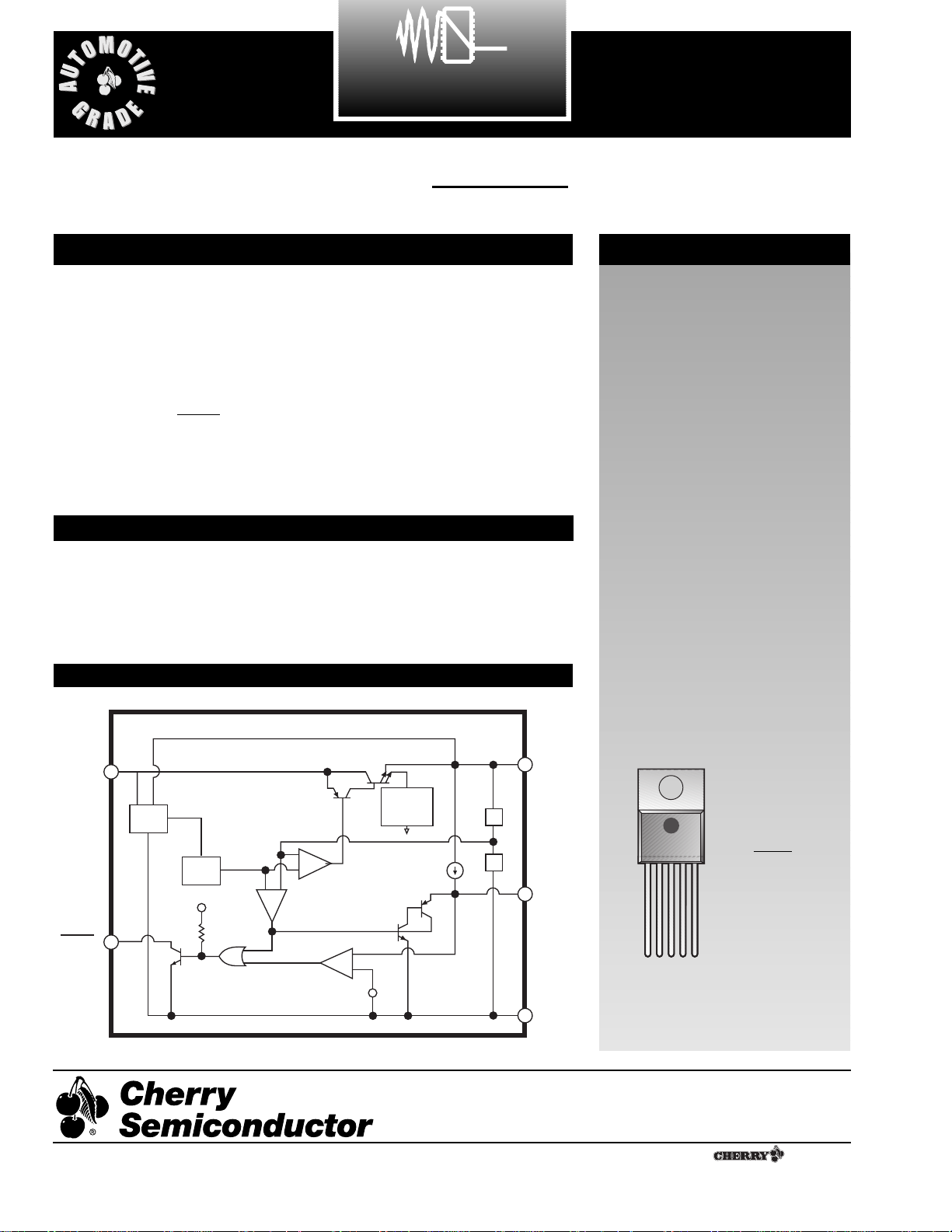
Block Diagram
Absolute Maximum Ratings
Forward Input Voltage ..................................................................................18V
Operating Junction Temperature, T
J
..............................................-40 to 150ûC
Storage Temperature........................................................................-55 to 150ûC
Lead Temperature Soldering
Wave Solder (through hole styles only)..........10 sec. max, 260¡C peak
Description
1. V
IN
2. RESET
3. Gnd
4. Delay
5. V
OUT
Rev. 2/18/98
Cherry Semiconductor Corporation
2000 South County Trail, East Greenwich, RI 02818
Tel: (401)885-3600 Fax: (401)885-5786
Email: info@cherry-semi.com
Web Site: www.cherry-semi.com
A Company
¨
V
IN
RESET
Start
REF
TO V
OUT
+-
Comparator
+
-
Error Amp
Low Voltage
INHIBIT
Comparator
Delay
V
OUT
Output
Current
Limit
I
CHARGE
SCR
Latch
-
+
V
CMP
Delay
Gnd
2
CS403
PARAMETER TEST CONDITIONS MIN TYP MAX UNIT
Electrical Characteristics : Refer to the test circuit, -40¡C ² T
C
² 125¡C, -40 ² TJ² 150¡C, 7V ² VIN² 10V unless otherwise specified
td = Cdx V
DTC/Ich
= C
Delay
x 2.105(typical)
where:
t
d
= Time delay
C
d
= Value of external charging capacitor (see test circuit).
V
DTC
= Delay threshold charge
I
ch
= Reset delay capacitor charging current.
Output Voltage, V
OUT
VIN= 8.5V, I
OUT
= 250mA
TJ= 25¡C 4.95 5.00 5.05 V
100mA ² I
OUT
² 750mA 4.85 5.00 5.15
Operating Input Voltage 100 to 750mA -0.75 18.0 V
Load Regulation 100mA ² I
OUT
² 750mA, VIN= 8.5V 30 100 mV
Dropout Voltage I
OUT
= 750mA 1.4 1.8 V
Quiescent Current I
OUT
= 0mA 3 4 mA
I
OUT
= 750mA 5 25 mA
PSRR I
OUT
-250mA f = 120Hz 70 dB
C
OUT
= 10µF, VIN= 8.5V±V
pp
Output Short Circuit Current 1 A
Reset Output Voltage IR= 1.6mA 1.0 ² V
OUT
² 4.75V 0.08 0.40 V
Reset Output Leakage Current V
OUT
in regulation 0 50 µA
Delay Time for Reset Output Cd= 100nF 10 20 30 ms
Reset Threshold: V
RTH
V
OUT
Increasing V
OUT
-0.04 V
V
RTL
V
OUT
Decreasing 4.75 V
Threshold Hysteresis 10 50 mV
Delay, V
DTC
Charge 3.7 4.0 4.4 V
Delay, V
DTD
Discharge 3.1 3.5 3.9 V
Delay Hysteresis, V
DH
200 500 1000 mV
Reset Delay Capacitor 10 20 40 µA
Charging Current, I
CH
Reset Delay Capacitor 0.6 1.2 V
Discharge Voltage, V
DIS
Package Lead Description
PACKAGE LEAD # LEAD SYMBOL FUNCTION
5 Lead TO-220
1V
IN
Input voltage.
2 CMOS compatible output lead. goes low whenever V
OUT
falls out of regulation.
3 Gnd Ground connection.
4 Delay Timing capacitor for function.
5V
OUT
Regulated output voltage, 5V (typ).
RESET
RESETRESET
 Loading...