

Cherry Semiconductor CS3972YN8, CS3972YDWR16, CS3972YDW16, CS3972YTVA5, CS3972YTHA5 Datasheet
...
1
CS3972
1.25A High Efficiency Switching Regulator
CS3972
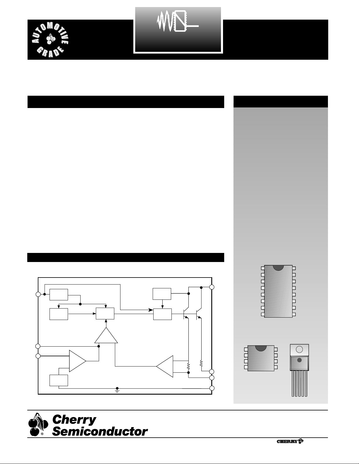
Description
Block Diagram
Features
■
75V
MAX
, 2A
PEAK
Internal
Switch
■
3V to 60V Input Voltage
Range
■
6mA Input Supply
Current
■
1.24V Precision Reference
■
40kHz Switching
Frequency
■
Variable Current Limit
with External Voltage
Clamp
■
Under-Voltage Protection
■
Over-Temperature
Protection
■
External Synchronization
Package Options
5L TO-220
Tab (Gnd)
8L PDIP
1
Gnd
V
C
V
FB
NC
E
2
V
SW
E
1
V
IN
1
1V
C
2V
FB
3 Gnd
4V
SW
5V
IN
16L SO Wide
1
GndNC
NC
NC
NC
V
IN
E
1
V
SW
E
2
V
C
V
FB
NC
NC
NC
NC
NC
The CS3972 is a 1.25A, 60V, current
mode, high efficiency, switching
regulator circuit. It can be configured in buck, boost, forward, isolated and non-isolated topologies,
using a single-ended switch.
The IC contains a 1.25A high efficiency output switch, precision
bandgap reference, voltage regulator, error amplifier, oscillator, control, and protection circuitry.
Output transistor efficiency is
achieved by keeping the switch in
quasi-saturation when it is on. This
minimizes the switch turn-off
delay time and power dissipation,
an important consideration for
applications with wide ranging
loads.
The precision reference is internally
trimmed to 1.24V, while the oscillator frequency is internally trimmed
to 40kHz. The on board 2.3V regulator powers the internal circuitry.
By keeping the voltage regulator at
2.3V, the IC is able to operate down
to 3V and maintain a constant input
supply current of 6mA(typ).
Synchronization mode is achieved
by applying a pulsating VCvoltage
of less than 0.2V with a duration of
about 0.5µs to VCpin. The switching frequency can be adjusted from
50kHz to 70kHz. The IC's synchronization mode is set externally.
Protection circuitry includes a variable current limit with external
voltage clamp, under-voltage and
over-temperature protection.
Rev. 6/23/99
Cherry Semiconductor Corporation
2000 South County Trail, East Greenwich, RI 02818
Tel: (401)885-3600 Fax: (401)885-5786
Email: info@cherry-semi.com
Web Site: www.cherry-semi.com
A Company
®
V
IN
2.3V
Reg
Output
Protection
V
SW
0.22Ω
1.25A,
75V
Switch
E2*
E1*
Gnd
40kHz
OSC
V
C
1.24V
Ref
-
+
Error
Amp
V
FB
*Always connect E1 to Ground Pin on DIP package. Both emitters are tied to ground on TO-220 Package.
COMP
+
Logic
Driver
-
+
Current
0.22Ω
Amp
-
2
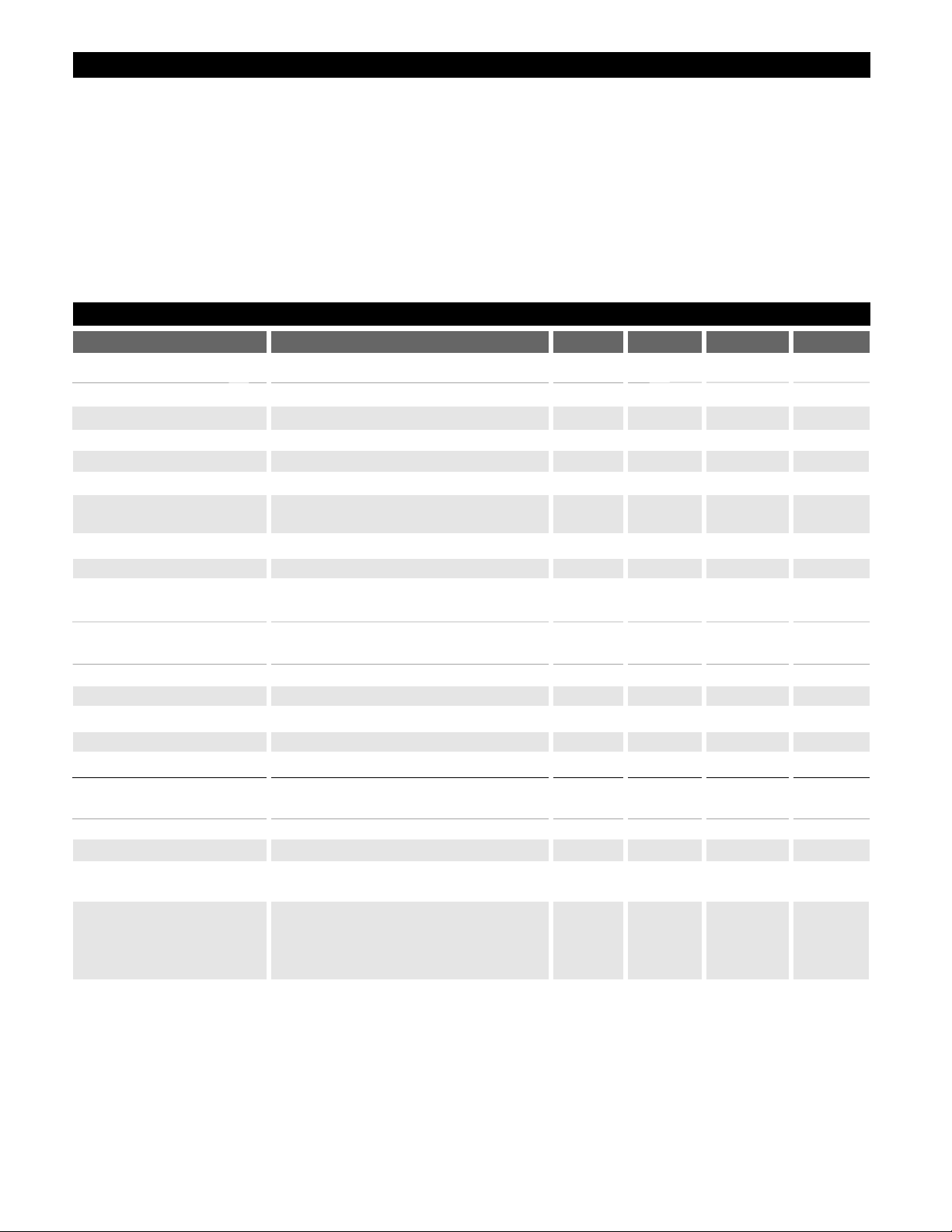
Absolute Maximum Ratings
CS3972
PARAMETER TEST CONDITIONS MIN TYP MAX UNIT
Input Voltage Range ........................................................................................................................................................3V to 60V
Output Switching Voltage.........................................................................................................................................................75V
Voltage Transient (t
r
=10µs, tf=400ms)......................................................................................................................................60V
ESD (Human Body Model; R=1.5kΩ, C=100pF) ...................................................................................................................2kV
Junction Temperature Range...............................................................................................................................-40°C to +150°C
Storage Temperature Range ................................................................................................................................-65°C to +150°C
Lead Temperature Soldering
Wave Solder (through hole styles only)......................................................................................10 sec. max, 260°C peak
Reflow (SMD styles only) ......................................................................................60 sec. max above 183°C, 230°C peak
Feedback Pin Voltage (1ms transient)...................................................................................................................................±15V
Electrical Characteristics:
For 3V≤VCC≤60V, -40°C≤TA≤125°C unless otherwise specified.
■
Reference Voltage VC=0.8V; VFB=V
REF
1.214 1.244 1.274 V
Line Regulation VC=0.8V; VFB=V
REF
, 3V≤VIN≤60V 0.03 %/V
Feedback Input Current VC=0.8V; VFB=V
REF
350 1100 nA
Minimum Input Voltage VC=VFB=V
REF
2.6 3.0 V
Supply Current VC=0.6V; 3V≤VIN≤60V 6.0 9.0 mA
Supply Current Increase
during switch on time VC=open, 1.0V≤VFB≤1.5V 25 mA/A
Switching Frequency VC=VFB=V
REF; VSW
=15V 33 40 47 kHz
Maximum Duty Cycle VC=2V; VFB=open, VSW=15V 92 %
VCThreshold VFB=open; VSW=15V, 0.60 0.90 1.25 V
duty cycle=0%
■ Error Amplifier
Transconductance VC=0.8V; VFB=V
REF
, ∆IC=±25µA 2400 4400 7000 µmho
Source/Sink Current VC=1.5V 120 200 400 µA
High Voltage Clamp VFB=1.0V 2.0 V
Low Voltage Clamp VFB=1.5V 0.38 V
Gain 0.9V≤VC≤1.4V, VFB=V
REF
800 V/V
■ Output Switch
Breakdown Voltage VC=0.5V; 3V≤VIN≤60V, I
OUT
=5mA 75 90 V
On Resistance VC=open, VFB=0.8V, I
OUT
=1.25A 0.6 1.0 Ω
Control Voltage to Switch 1.2V≤VC≤1.8V 2 A/V
Current Transconductance
Current Limit Duty Cycle≤50%, TJ≥25°C 1.25 3.00 A
Duty Cycle≤50%, TJ<25°C 1.25 3.50 A
Duty Cycle=80% 1.00 2.50 A
Duty Cycle=80% (Note 1) 0.50 2.50 A
Note 1: 16 lead SO wide package only.
 Loading...