

Cherry Semiconductor CS3750ENF16 Datasheet
1
Features
OUT1A
Thermal
Shutdown
V
REF
Overvoltage
1/2 H -Bridge
Driver
with Current
Limit
RC Filter
for PWM Input
OUT1B C1
1/2 H -Bridge
Driver
with Current
Limit
DIRECTION
Control
1/2 H- Bridge
Driver
with Current
Limit
RC Filter
for PWM Input
1/2 H- Bridge
Driver
with Current
Limit
DIRECTION
Control
OUT2A OUT2B C2
Gnd
IN2DIR2IN1DIR1V
S1,2
■ 2 Independent NPN
H-Bridge Drivers
■ No Analog Trim Required
■ Used in Multiplexed
Systems
■ Quiet Gauge Operation
■ Programmable Slew
Rate Minimizes
Switching Noise
■ Fault Protection
Over Voltage
Thermal Shutdown
Short Circuit
Package Options
16 Lead PDIP
(internally fused leads)
CS3750
100mA Dual H-Bridge Air-Core
Gauge Driver
1
DIR1
C1
IN1
Gnd
Gnd
OUT1A
VS1
OUT1B
DIR2
C2
IN2
Gnd
Gnd
OUT2A
VS2
OUT2B
Description
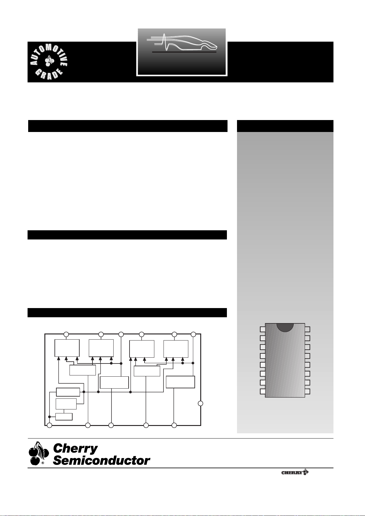
Block Diagram
Absolute Maximum Ratings
The CS3750 is a dual H-bridge four
quadrant air-core gauge driver. The IC
provides all the functions necessary to
drive a tachometer or speedometer as
part of a microprocessor based multiplexed system. Digital input control
eliminates the need for any analog calibration of the gauge.
The controlling microprocessor sends
out a PWM signal to each H bridge
driver input (IN1, IN2). The PWM signal duty cycle is proportional to the
HÐbridge output. Output current
(100mA max) direction is controlled by
the DIRECTION input. PWM switching noise is minimized at each half
bridge by an internal RC filter and
external programmable capacitor.
The CS3750 is protected against 50V
load dump, over voltage and thermal
runaway fault conditions. Any of these
faults causes the IC to shut down. Each
high side of the output driver is current
limited. A short circuit condition in one
driver does not affect the others.
CS3750
Supply Voltage .................................................................................7.5V to +16V
Internal Power Dissipation.....................................................Internally limited
Logic Input Voltages.......................................................................Ð0.3V to 6.5V
Junction Temperature Range ...................................................Ð40¡C to +150¡C
Storage Temperature Range.....................................................Ð55¡C to +165¡C
Lead Temperature Soldering
Wave Solder (through hole styles only)...........10 sec. max, 260¡C peak
Electrostatic Discharge (Human Body Model)............................................8kV
Rev. 7/20/95
Cherry Semiconductor Corporation
2000 South County Trail, East Greenwich, RI 02818
Tel: (401)885-3600 Fax: (401)885-5786
Email: info@cherry-semi.com
Web Site: www.cherry-semi.com
A Company
¨
2
Electrical Characteristics: 7.5V <= VCC<=15V; -40¡C ² TA² +85¡C unless otherwise specified.
PARAMETER TEST CONDITIONS MIN TYP MAX UNIT
CS3750
Note 1: Time required for output signal to rise to 90% of its amplitude after input signal switches.
Note 2: Time required for output signal to decrease to 10% of its amplitude after input signal switches.
■ Output Stage
V
OUT
Saturation Voltage I
OUT
=100mA; VIN=0V 0.25 0.50 V
(Low Side) I
OUT
=1mA; VIN=0V 0.01 0.10 V
V
OUT
Offset Voltage VC=5V; I
OUT
=-30mA 15 50 mV
V
OUT
Saturation High Side VIN=5V;I
OUT
=-100mA VS-2 VS-1.5 VS V
Low Side VIN=0V;I
OUT
=-1mA 0.02 0.10 V
V
OUT
Differential VC=5V, I
OUT
=-100mA 100 mV
Matching Voltage
Supply Current VIN=V
DIR
=0; 23 45 mA
■ Input Stage
VINLOW VINdecreasing; V
DIR
=0V 0.8 1.9 V
HIGH V
IN
increasing; V
DIR
=0V 2.0 3.5 V
Hysteresis V
DIR
=0V 100 mV
IINLOW VIN=0.8V; V
DIR
=0V 20 100 µA
HIGH VIN=3.5V 0.4 100.0 µA
Output Slew Rate VIN=250Hz; R
LOAD
=150½ 0.2 0.8 V/us
with respect to input
Output Turn on Delay VIN=250Hz; R
LOAD
=150½, note 1 1.5 6 µs
with respect to input
Output Turn off Delay VIN=250Hz; R
LOAD
=150½, note 2 2.4 9 µs
with respect to input
■ Direction
V
DIR
LOW VIN=5V; V
DIR
decreasing 0.8 1.9 V
HIGH VIN=5V; V
DIR
increasing 2.0 3.5 V
Hysteresis VIN=5V 100 mV
I
DIR
LOW VIN=0V; V
DIR
=0.8V 40 100 µA
HIGH VIN=0V; V
DIR
=3.5V 0.4 100 µA
Output Slew Rate VIN=5V; f
DIR
=250Hz; C=0µF 0.2 1.5 V/µs
with respect to DIR
Output Fall Time VIN=0V; V
DIR
=0V; C=0µF 0.2 2.0 µs
with respect to DIR
Output Turn on Delay VIN=5V; R
LOAD
=150½
with respect to DIR V
DIR
=250Hz; C=0µF, note 1 1 6 µs
Output Turn off Delay VIN=5V; R
LOAD
=150½
with respect to DIR V
DIR
=250Hz; C=0µF, note 2 2.5 9 µs
■ Protection Functions
I
OUT
Current Limit VIN=5V 100 225 mA
(High Side Only)
Over Voltage Threshold VIN=5V 17.0 21.5 26.0 V
Hysteresis 0.5 V
Thermal Shutdown 160 ¡C
Hysteresis 20 ¡C
 Loading...