

Cherry Semiconductor CS3524AGNWR16, CS3524AGNW16, CS3524AGN16 Datasheet
1
Features
V
IN
SYNC
C
T
COMP
I
SENSE
+
V
OUT
A
R
T
V
OUT
B
E
B
Gnd
EA-
EA+
I
SENSE
-
SHUTDOWN
E
A
V
REF
-
+
+
-
COMP
EA
CL
5V Reference
Regulator
Flip
Flop
PWM
Latch
OSC
UV
Sense
Power to
Internal
Circuitry
T
R
S
CLOCK
S
RAMP
V
IN
V
IN
200mV
1kΩ
10kΩ
■
Precision Reference
Internally Trimmed to ±1%
■
Current Limit
■ Undervoltage Lockout
■ Start-up Supply Current
< 4mA
■ Output to 200mA
■ 60V Output Capability
■ Wide Common-mode
Input Range for Error and
Current Limit Amplifiers
■ PWM Latch Insures Single
Pulse per Period
■ Double Pulse Suppression
■ 200ns Shutdown
■ Guaranteed Frequency
■ Thermal Shutdown
Package Options
16 Lead PDIP & SO Wide
CS3524A
Voltage Mode PWM Control Circuit
with 200mA Output Drivers
16
15
14
13
12
11
11
10
9
1
2
3
4
5
6
7
8
EA-
EA
+
SYNC
I
SENSE
+
I
SENSE
-
R
T
C
T
Gnd
V
REF
V
IN
E
B
V
OUT
B
V
OUT
A
E
A
SHUTDOWN
COMP
CS3524A
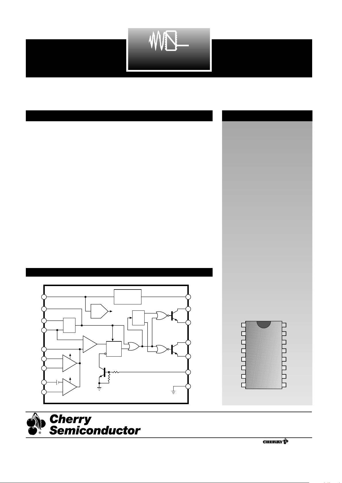
Description
Block Diagram
The CS3524A PWM control circuit
retains the same versatile architecture
of the industry standard CS3524
(SG3524) while adding substantial
improvements.
The CS3524 is pin-compatible with
“non-A” versions, and in most applications can be directly interchanged. The
CS3524A, however, eliminates many of
the design restrictions which had previously required additional external
circuitry.
The CS3524A includes a precision 5V
reference trimmed to ±1% accuracy
(eliminating the need for potentiometer
adjustments), an error amplifier with
an output voltage swing extending to
5V, and a current sense amplifier useful in either the ground or power supply output lines. The uncommitted
60V, 200mA NPN output pair greatly
enhances the output drive capability.
The CS3524A features an undervoltage
lockout circuit which disables all internal circuitry (except the reference) until
the input voltage has risen to 8V. This
holds standby current low until turnon, and greatly simplifies the design of
low power, off-line supplies. The turnon circuit has approximately 600mV of
hysteresis for jitter free activation.
Other improvements include a PWM
latch that insures freedom from multiple pulsing within a period, even in
noisy environments; logic to eliminate
double pulsing on a single output, a
200ns external shutdown capability,
and automatic thermal protection from
excessive chip temperature. The oscillator circuit is usable to 500kHz and is
easier to synchronize with an external
clock pulse.
A Company
®
Rev. 10/28/96
Cherry Semiconductor Corporation
2000 South County Trail, East Greenwich, RI 02818
Tel: (401)885-3600 Fax: (401)885-5786
Email: info@cherry-semi.com
Web Site: www.cherry-semi.com
2
Electrical Characteristics: 0˚C ≤ T
A
≤ +70˚C for the CS3524A; VIN= VCC= 20V; unless otherwise stated.
PARAMETER TEST CONDITIONS MIN TYP MAX UNIT
Absolute Maximum Ratings
Supply Voltage (VIN).................................................................................................................................................................40V
Collector Supply Voltage (VCC) ...............................................................................................................................................60V
Output Current (Each Output)...........................................................................................................................................200mA
Reference Output Current.....................................................................................................................................................50mA
Oscillator Charging Current ..................................................................................................................................................5mA
Power Dissipation at TA=25˚C.........................................................................................................................................1000mW
Power Dissipation at TJ=+25˚C........................................................................................................................................2000mW
Derate for Case Temperature above +25˚C........................................................................................................16mW/˚C
Storage Temperature Range ................................................................................................................................-65˚C to +150˚C
Lead Temperature Soldering: Wave Solder (through hole styles only)..........................................10 sec. max, 260°C peak
Reflow (SMD styles only) ......................................................................................60 sec. max above 183°C, 230°C peak
CS3524A
■ Turn-on Characteristics
Input Voltage Operating range after Turn-on 8 40 V
Turn-on Threshold 5.5 7.5 8.5 V
Turn-on Current VINTurn-on - 100mV 2.5 4.0 mA
Operating Current VIN= 8 to 40V 5 10 mA
Turn-on Hysteresis* 0.6 V
■ Reference Section
Output Voltage TA= 25˚C 4.90 5.00 5.20 V
Line Regulation VIN= 10 to 40V 10 30 mV
Load Regulation IL= 0 to 20mA 20 50 mA
Temperature Stability* Over Operating Range 20 50 mV
Short Circuit Current V
REF
= 0, TA= 25˚C 80 100 mA
Output Noise Voltage* 10Hz ≤ f ≤ 10kHz, TA= 25˚C 40 µVrms
Long Term Stability* TA= 125˚C; 1000 Hrs. 20 50 mV
■ Oscillator Section (Unless otherwise specified, R
T
= 2700Ω, CT= 0.01µF)
Initial Accuracy TA= 25˚C394347kHz
Temperature Stability* Over Operating Temperature Range 1 2 %
Minimum Frequency RT= 150kΩ, CT= 0.1µF 120 Hz
Maximum Frequency RT= 2.0kΩ, CT= 470pF 500 kHz
Output Amplitude* TA= 25˚C 3.5 V
Output Pulse Width* TA= 25˚C 0.5 µs
Ramp Peak 3.3 3.5 3.7 V
Ramp Valley 0.7 0.9 1.0 V
■ Error Amplifier Section (Unless otherwise specified, V
CM
= 2.5V)
Input Offset Voltage 2 10 mV
Input Bias Current 1 10 µA
Input Offset Current 0.5 1.0 µA
Common Mode
Rejection Ratio VCM= 1.5 to 5.5V 60 75 dB
Power Supply Rejection Ratio VIN= 10 to 40V 50 60 dB
Output Swing Minimum Total Range 0.5 5.0 V
* These parameters are guaranteed by design but not 100% tested in production.
 Loading...