

Cherry Semiconductor CS3361YDR14, CS3361YD14 Datasheet
Features
■ Drives Logic Level Power
NFET
■ 80V Load Dump
■ Temperature Compensated
Regulation Voltage
■ Shorted Field Protection
Duty Cycle, Self Clearing
Package Options
CS3361
Alternator Voltage Regulator
FET Driver
CS3361
Description
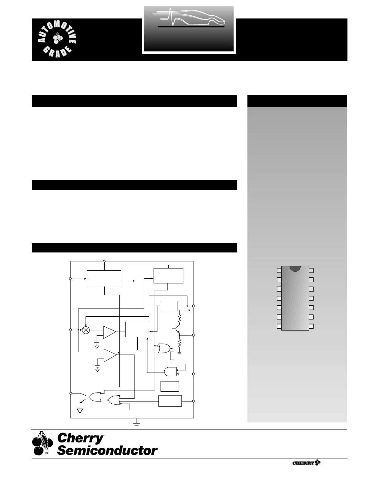
The CS3361 integral alternator regulator integrated circuit provides
the voltage regulation for automotive, 3-phase alternators.
It drives an external logic level N
channel enhancement power FET
for control of the alternator field
current. In the event of a charge
fault, a lamp output pin is provided
to drive an external darlington transistor capable of switching on a
fault indicator lamp. An overvoltage or no Stator signal condition
activates the lamp output.
The CS3361 is available in a 14 lead
SO package.
Block Diagram
Absolute Maximum Ratings
Storage Temperature Range .....................................................-55°C to +165°C
Junction Temperature Range....................................................-40°C to +150°C
Continuous Supply..........................................................................................27V
I
CC
Load Dump .........................................................................................400 mA
Lead Temperature Soldering
Reflow (SMD styles only)............60 sec. max above 183°C, 230°C peak
DD
Gnd
NC
OSC
Lamp
NC
NC
SC
NC
V
CC
Sense
IGN
STATOR
NC
14 Lead SO
1
A Company
®
Rev. 1/29/99
Cherry Semiconductor Corporation
2000 South County Trail, East Greenwich, RI 02818
Tel: (401)885-3600 Fax: (401)885-5786
Email: info@cherry-semi.com
Web Site: www.cherry-semi.com
V
CC
ENABLE
IGN
Series
Regulator
Load Dump
Detection and
VSUP
Protection
1
Sense
LAMP
OSC
Lamp
Gnd
R
S
Indicator
STATOR
Power Up
STATOR
Timer
DELAY
+
–
+
–
VREG
+
–
VHV
R
RS Flop
Set
Dominate
VSUP
Q
VSUP
ENABLE
OSC
Device
Driver
SC
STATOR
2
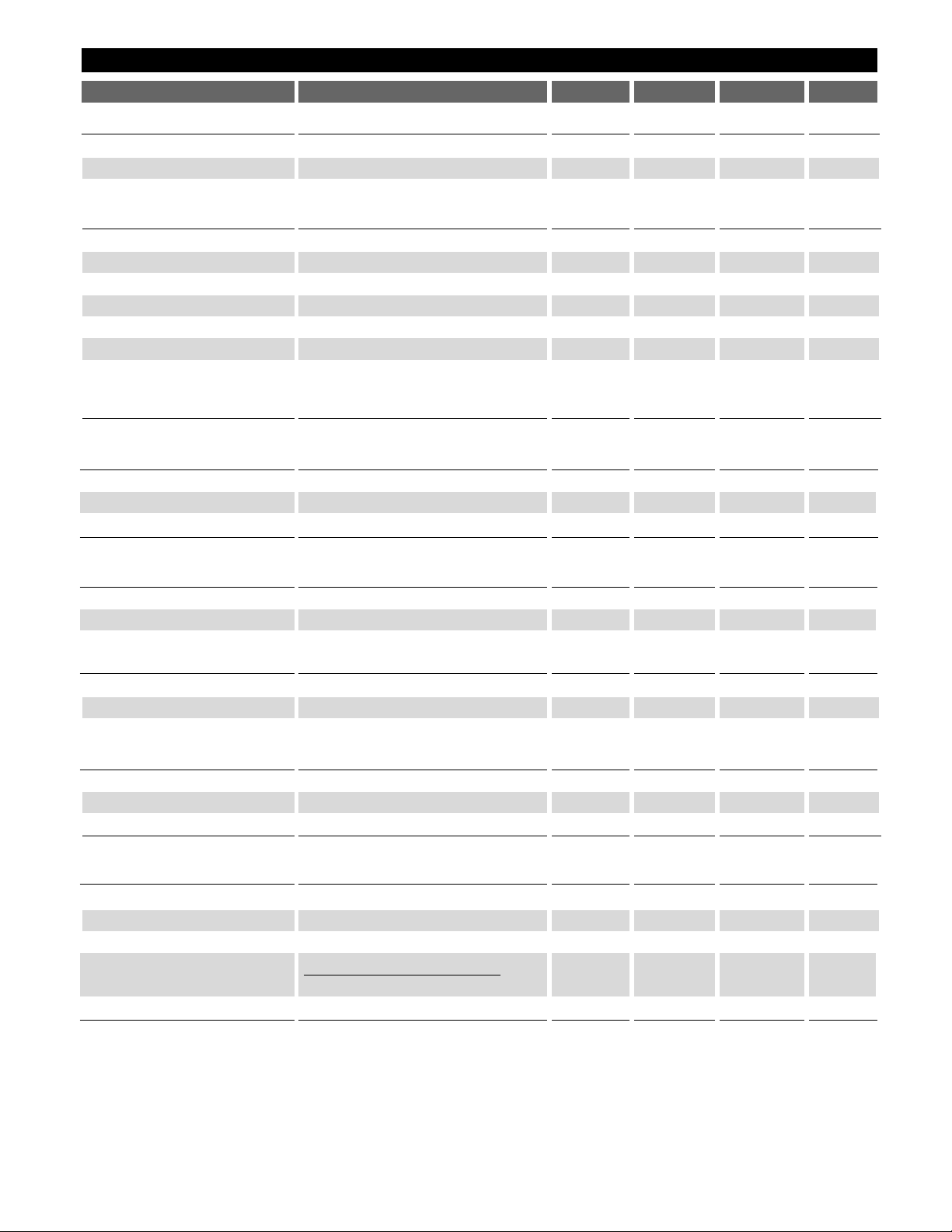
Electrical Characteristics: -40°C < TA< 125°C, -40°C < TJ< 150°C, 9V ≤ VCC≤ 17V; unless otherwise specified.
PARAMETER TEST CONDITIONS MIN TYP MAX UNIT
CS3361
■ Supply
Supply Current Enabled – 10 mA
Supply Current Disabled – 50 µA
■ Driver Stage
Output High Voltage 5.5 12 V
Output High Current VDD= 1.2V -10 -6 -4 mA
Output Low Voltage IOL= 25µA – 0.35 V
Minimum ON Time C
OSC
= 0.022µF 200 µs
Minimum Duty Cycle – 6 10 %
Short Circuit Duty Cycle 1 5 %
Field Switch Turn On
Rise Time 15 75 µs
Fall Time 15 75 µs
■ Stator
Input High Voltage 10 V
Input Low Voltage – 6 V
Stator Time Out High to Low 6 100 600 ms
■ Lamp
Output High Current V
LAMP
@ 3V – 50 µA
Output Low Voltage I
LAMP
@ 30mA – 0.35 V
■ Ignition
Input High Voltage ICC> 1mA 1.8 – V
Input Low Voltage ICC< 100µA – 0.5 V
■ Oscillator
Oscillator Frequency C
OSC
= 0.022µF 90 210 Hz
Rise Time/Fall Time C
OSC
= 0.022µF 17 – –
Oscillator High Threshold C
OSC
= 0.022µF – 4.5 V
■ Battery Sense
Input Current -10 +10 µA
Regulation Voltage @25°C, R
1
= 100kΩ, R2= 50kΩ 13.8 15.8 V
Proportional Control 0.10 0.25 V
High Voltage V
High Voltage
@ Lamp On 1.083 1.190
Threshold Ratio V
Regulation
@ 50% Duty Cycle
High Voltage Hysteresis 0.020 0.600 V
 Loading...