

Cherry Semiconductor CS294GN8, CS294GDR8, CS294GD8 Datasheet
-
+
-
+
V
FB
Signal
Common
Filter
20kW
10kW
Bias
Gnd
Detect
4.7kW
50kW
Amp
OUT
+V
S
SCR
Trigger
-
+
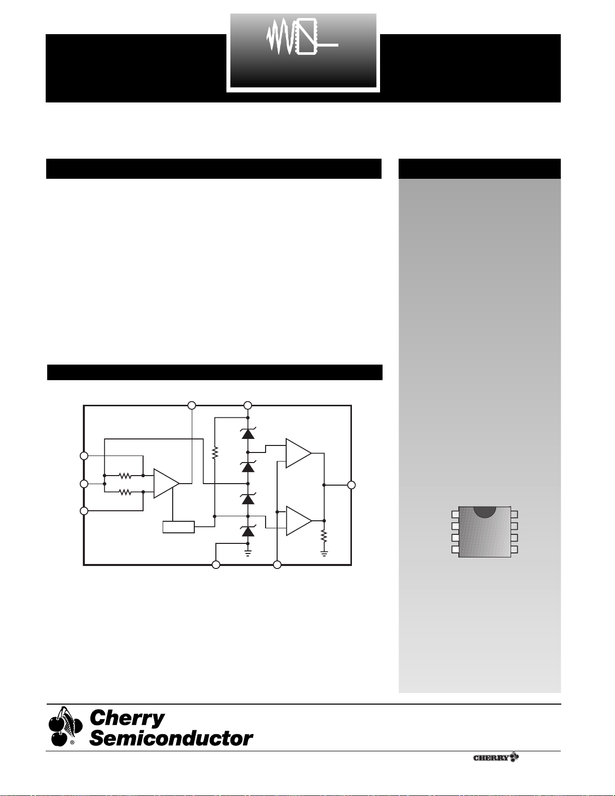
The CS294 is an AC outlet ground
fault interrupter controller IC. The
IC detects the presence of hazardous grounding conditions and
open circuits the AC line before a
dangerous shock can occur.
The CS294 contains an operational
amplifier, an SCR driver and a 24V
zener shunt regulator. Two sense
coils, a bridge rectifier, a relay and
an SCR are required as external
components. The completed interrupter circuit can detect and protect
against both hot wire to ground
faults and neutral wire to ground
faults.
The CS294 is built on a 30V bipolar
process and is available in 8 lead
DIP packages.
Features
■ Supply Derived from
AC Supply Ñ 24V
■ Direct Interface to SCR
■ Adjustable Sensitivity
■ Grounded Neutral Fault
Detection
Package Options
CS294
Ground Fault Interrupter
CS294
Description
Block Diagram
V
FB
Filter
Signal Common
Gnd
Detect
Amp
OUT
+V
S
SCR Trigger
8 Lead PDIP & SO Narrow
1
Rev. 1/20/99
Cherry Semiconductor Corporation
2000 South County Trail, East Greenwich, RI 02818
Tel: (401)885-3600 Fax: (401)885-5786
Email: info@cherry-semi.com
Web Site: www.cherry-semi.com
A Company
¨
1
V
FB
Error Amp Inverting Input 30V -0.3V N/A 20mA
Filter Error Amp Non-Inverting Input 30V -0.3V 1mA 1mA
Signal Common Signal Reference Input V(+VS) + 1V V(+VS) - 1V 1ma 1ma
Gnd Power Supply Return 0V 0V 1mA 10mA
SCR Trigger SCR Driver Output 30V -0.3V 1mA 1mA
+V
S
Shunt Regulator Supply Input 30V -0.3V 1mA 1mA
Amp
OUT
Error Amp Output 30V -0.3V 1mA 1mA
Detect Ground Fault Detect Input 6V -0.3V 10mA 10mA
Electrical Characteristics:
TA= 25¡C.
For ease of testing and improved test accuracy, Signal Common is grounded and a negative voltage is applied to the Gnd pin.
PARAMETER TEST CONDITIONS MIN TYP MAX UNIT
CS294
2
Absolute Maximum Ratings
Pin Symbol Pin Name V
MAX
V
MIN
I
SOURCE
I
SINK
Operating Junction Temperature, TJ. . . . . . . . . . . . . . . . . . . . . . . . . . . . . . . . . . . . . . . . . . . . . . . . . . . . . . . . . . . . . . . . . 150¡C
Lead Temperature Soldering:
Wave Solder (through hole styles only) . . . . . . . . . . . . . . . . . . . . . . . . . . . . . . . . . . . . . . . . . . 10 Sec. max 260ûC Peak
Reflow (SMD styles only) . . . . . . . . . . . . . . . . . . . . . . . . . . . . . . . . . . . . . . . . . . . 60 sec. max above 183¡C, 230¡ peak
Storage Temperature Range, TS. . . . . . . . . . . . . . . . . . . . . . . . . . . . . . . . . . . . . . . . . . . . . . . . . . . . . . . . . . . . . -65¡C to 150¡C
Supply Current +V
S
1.2 mA
Negative Supply Voltage Clamp -14.1 -11.9 -9.7 V
Positive Supply Voltage Clamp 9.7 11.9 14.1 V
Output Offset Voltage -400 67 +1100 mV
Output Resistance I(SCR Trigger) = 100µA 2.89 4.70 6.78 k½
Negative Amp Output Swing -10.95 -8.5 V
Positive Amp Output Swing 8.5 11.5 V
Positive Detect Threshold 5.9 6.5 7.2 V
Negative Detect Threshold -7.2 -6.5 -5.9 V
Detect Leakage Current V(SCR Trigger) = 0V 0.5 5.0 µA
Amplifier Open Loop Gain V(VFB) = 1mV RMS @ 50kHz 20 90 V/V
Operating Temperature Range TA(Note 1) 0 70 ¡C
Note 1: Guaranteed by design.
 Loading...