

Cherry Semiconductor CS289GN14, CS289GDWFR20, CS289GDWF20 Datasheet
Features
■
Single Supply Operation
■
On-Chip Regulation
■
20mA Output Drive
Capability
Package Options
20L SOIC Wide
(internally fused leads)
14L PDIP
CS289
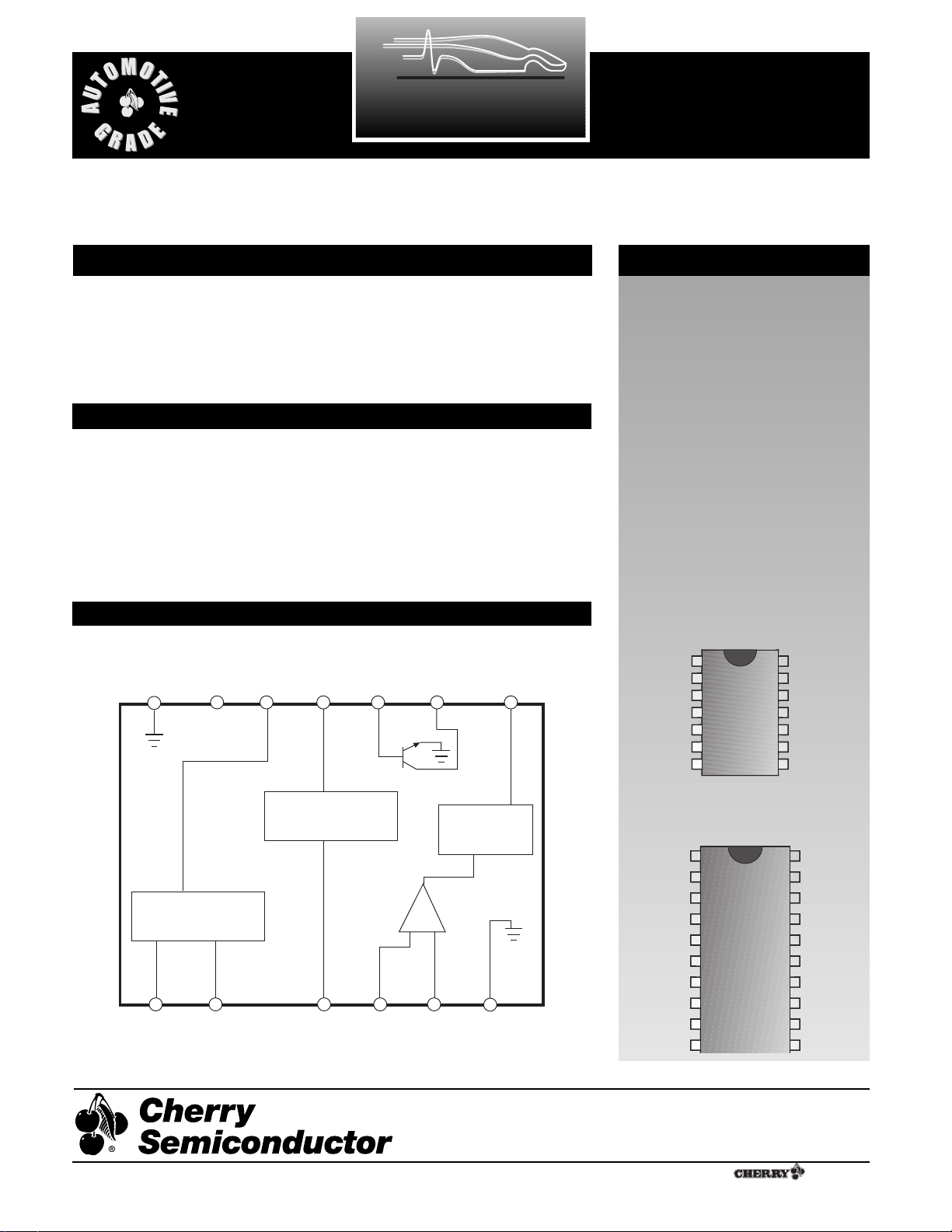
20mA Air-Core Tachometer Drive Circuit
1
V
Z
V
SINE
V
BIAS
Gnd
C
P
Ð
CP+
NC
V
CC
V
COS
V
REG
SQIN
S
Q
OUT
F/V
OUT
Gnd
Gnd
Gnd
Gnd
Gnd
Gnd
Gnd
1
V
Z
V
SINE
V
BIAS
Gnd
C
P
Ð
C
P
+
NC
Pwr Gnd
V
CC
V
COS
V
REG
SQIN
S
Q
OUT
F/V
OUT
CS289
Description
The CS289 is specifically designed
for use with air-core meter movements. The IC has charge pump circuitry for frequency-to-voltage conversion, a shunt regulator for stable
operation, a function generator, and
sine and cosine amplifiers. The
buffered sine and cosine outputs
will typically sink or source 20mA.
Block Diagram
Absolute Maximum Ratings
Supply Voltage (VCC)......................................................................................20V
Operating Temperature ............................................................Ð40¡C to +100¡C
Junction Temperature..................................................................Ð40¡C to 150¡C
Storage Temperature.................................................................Ð65¡C to +150¡C
Lead Temperature Soldering
Wave Solder (through hole styles only)...........10 sec. max, 260¡C peak
Reflow (SMD styles only)............60 sec. max above 183¡C, 230¡C peak
1
Rev. 3/8/99
Cherry Semiconductor Corporation
2000 South County Trail, East Greenwich, RI 02818
Tel: (401)885-3600 Fax: (401)885-5786
Email: info@cherry-semi.com
Web Site: www.cherry-semi.com
A Company
¨
Pwr Gnd
V
CC
V
COS
V
SQIN F/V OUT
REG
SQOUT
Regulator
Charge
Pump
Function
Generator
V
Z
SINE
V
BIAS
CpÐ GndV
+Ð
CP+
2
Package Pin Description
PACKAGE PIN # PIN SYMBOL FUNCTION
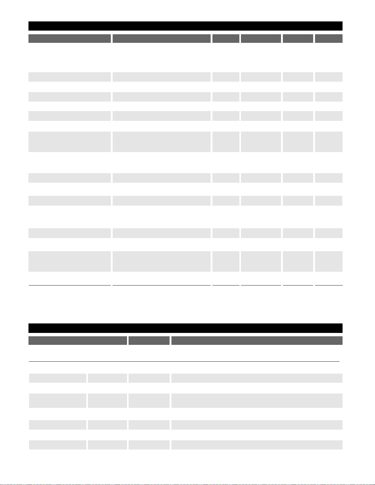
Electrical Characteristics: (VCC= 13.1V, -30¡C ² TA² 85¡C)
PARAMETER TEST CONDITIONS MIN TYP MAX UNIT
CS289
20L SO
(internally fused leads) 14L PDIP
11V
Z
External Zener reference.
22V
sine
Sine output signal.
34V
BIAS
Test pin or "0" calibration pin.
4, 5, 6, 7, 7 Gnd Analog Ground connection.
14, 15, 16, 17
85C
PÐ
Negative input to charge pump.
96C
P+
Positive input to charge pump.
10 3 NC No Connection
11 8 F/V
OUT
Output voltage proportional to input signal frequency.
Supply Current (Note 2) V
CC
= 15.0V 54 mA
V
CC
= 13.1V 60 65 mA
V
CC
= 11.3V 60 65 mA
Regulated Voltage I
REG
= 4.3mA 7.7 8.5 9.3 V
Regulation I
REG
= 0 to 5mA 0.10 0.20 V
Signal Input Current T = 25¡C 0.1 2.0 4.0 mA
Saturation Voltage I
SQ
OUT = 5mA, ISQIN = 500µA 0.20 0.55 V
Leakage Current I
SQ
OUT = 16V, VSQIN = 0V 10 µA
Input Current C
P
+ = 0, T = 25¡C 1 15 nA
F to V Output V
SQ
IN = 0 (zero input), Æ = 0¡ 1.8 2.1 2.4
V
COS
= 0 (Note 1), Æ = 270¡ 6.3 7.1 7.9 V
Linearity E
O
vs. Frequency
V
COS
= 0 (Note 1), Æ = 270¡, T = 25¡C -1.5 1.5 %
V
sine
at Æ = 0¡ VSQIN = 0 (zero input), Æ = 0¡ -0.55 0.00 0.55 V
MAX V
sine+
V
COS
= 0 (Note 1), Æ=90¡ 3.8 4.5 5.8 V
MAX V
sine-
V
COS
= 0 (Note 1), Æ = 270¡ -3.8 -4.5 -5.8 V
Coil Drive Current V
COS
= 0 (Note 1), Æ = 90¡, T = 25¡C 20 25 mA
V
COS
= 0 (Note 1), Æ = 270¡ 20 25 mA
MAX V
COS+
VSQIN = 0 (zero input), Æ = 0¡ 3.8 4.5 5.8 V
MAX V
COS-
V
sine
= 0 (Note 1), Æ = 180¡ -3.8 -4.5 -5.8 V
Coil Drive Current V
SQ
IN = 0 (zero input), Æ = 0¡ 20 25 mA
V
sine
= 0 (Note 1), Æ = 180¡ 20 25 mA
External Voltage Ref. 4.98 5.40 5.85 V
Note 1: V
sine
measured V
sine
to VZ. V
COS
measured V
COS
to VZ. All other voltages specified are measured to ground.
Note 2: Max PWR dissipation ²V
CC
X ICC- (V2I
sine
+ V12 I
COS
).
 Loading...