

Cherry Semiconductor CS2841BEN8, CS2841BEDR14, CS2841BED14 Datasheet
1
■ Optimized for
Off-line
Control
■ Internally Trimmed
Temperature
Compensated Oscillator
■ Maximum Duty-cycle
Clamp
■ V
REF
Stabilized before
Output Stage Enabled
■ Low Start-up Current
■ Pulse-by-pulse Current
Limiting
■ Improved Undervoltage
Lockout
■ Double Pulse Suppression
■ 1% Trimmed Bandgap
Reference
■ High Current Totem Pole
Output
Package Options
8 Lead PDIP
10
7
14
13
12
8
1
2
3
4
5
6
11
9
COMP
NC
V
FB
NC
Sense
NC
OSC
V
REF
NC
V
CC
V
CC
Pwr
V
OUT
Pwr Gnd
Gnd
14 Lead SO Narrow
CS2841B
Automotive Current Mode PWM
Control Circuit
CS2841B
Description
The CS2841B provides all the necessary features to implement offline fixed frequency current-mode
control with a minimum number of
external components.
The CS2841B (a variation of the
CS-2843A) is designed specifically
for use in automotive operation.
The low start threshold voltage of
8.0V (typ), and the ability to survive 40V automotive load dump
transients are important for automotive subsystem designs. The
CS-2841 series has a history of
quality and reliability in automotive applications.
The CS2841B incorporates a precision temperature-controlled oscillator with an internally trimmed
discharge current to minimize variations in frequency. Duty-cycles
greater than 50% are also possible.
On board logic ensures that V
REF
is
stabilized before the output stage
is enabled. Ion implant resistors
provide tighter control of undervoltage lockout.
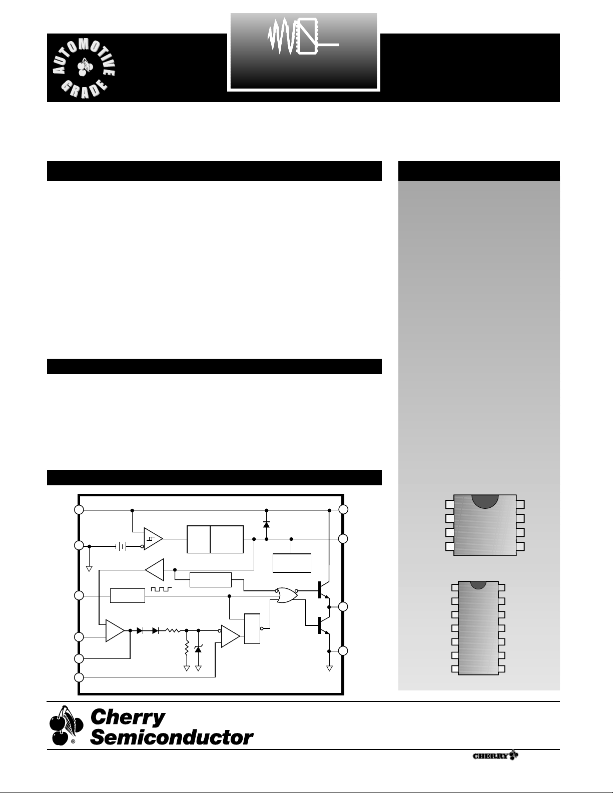
Block Diagram
Absolute Maximum Ratings
Supply Voltage (Low Impedance Source)...................................................40V
Output Current ...............................................................................................±1A
Output Energy (Capacitive Load) .................................................................5µJ
Analog Inputs (V
FB
, Sense) ............................................................-0.3V to 5.5V
Error Amp Output Sink Current...............................................................10mA
Lead Temperature Soldering
Wave Solder (through hole styles only) ..........10 sec. max, 260°C peak
Reflow (SMD styles only)...........60 sec. max above 183°C, 230°C peak
Features
Rev. 6/23/99
Cherry Semiconductor Corporation
2000 South County Trail, East Greenwich, RI 02818
Tel: (401)885-3600 Fax: (401)885-5786
Email: info@cherry-semi.com
Web Site: www.cherry-semi.com
A Company
®
V
Gnd
OSC
V
COMP
Sense
CC
8.0V/7.4V
+
FB
–
Amplifier
2.50V
Oscillator
Error
Undervoltage
Lock-out Circuit
V
C
2 R
R
Set/
Reset
Reference
Output
Enable
1 V
5V
Current
Sensing
Comparator
Internal
Bias
NOR
S
PWM
R
Latch
VCC Pwr
V
REF
V
OUT
Pwr Gnd
1
COMP
2
V
FB
3
Sense
4
OSC
8
V
7
V
6
V
5
Gnd
REF
CC
OUT

2
Electrical Characteristics: d -40≤TA≤85˚C RT=680kΩ, CT=0.022µF for triangular mode, VCC=15V (Note 1),
R
T
=10kΩ, CT=3.3nF for sawtooth mode (See Fig. 3), unless otherwise stated.
PARAMETER TEST CONDITIONS MIN TYP MAX UNIT
CS2841B
Notes: 1. Adjust Vccabove the start threshold before setting at 15V. 3. Parameter measured at trip point of latch with VFB=0.
2.These parameters, although guaranteed, are not 100% tested in production. 4. Gain defined as:
A = ; 0 ≤ V
Sense
≤ 0.8V.
∆V
COMP
∆V
Sense
■ Reference Section
Output Voltage TJ=25˚C, I
OUT
=1mA 4.90 5.00 5.10 V
Line Regulation 8.4≤VCC≤16V 6 20 mV
Load Regulation 1≤I
OUT
≤20mA 6 25 mV
Temperature Stability (Note 2) 0.2 0.4 mV/˚C
Total Output Variation Line, Load, Temp. (Note 2) 4.82 5.18 V
Output Noise Voltage 10Hz≤f≤10kHz, TJ=25˚C (Note 2) 50 µV
Long Term Stability TA=125˚C, 1000 Hrs. (Note 2) 5 25 mV
Output Short Circuit TA=25˚C -30 -100 -180 mA
■ Oscillator Section
Initial Accuracy Sawtooth Mode: (See Fig. 3)TJ=25˚C 47 52 57 kHz
Sawtooth Mode: -40˚C≤TA≤+85˚ 44 52 60 kHz
Triangular Mode (See Fig. 3) TJ=25˚C 44 52 60 kHz
Voltage Stability 8.4V≤Vcc≤16V 0.2 1.0 %
Temperature Stability Sawtooth Mode T
MIN≤TA≤TMAX
5%
Triangular Mode T
MIN≤TA≤TMAX
8%
(Note 2)
Amplitude V
OSC
(peak to peak) 1.7 V
Discharge current TJ=25˚C 7.4 8.3 9.2 mA
T
MIN≤TA≤TMAX
7.2 9.4 mA
■ Error Amp Section
Input Voltage V
COMP
=2.5V 2.42 2.50 2.58 V
Input Bias Current VFB=0V -0.3 -2.0 µA
A
VOL
2≤V
OUT
≤4V 65 90 dB
Unity Gain Bandwidth (Note 2) 0.7 1.0 MHz
PSRR 8.4V≤VCC≤16V 60 70 dB
Output Sink Current VFB=2.7V, V
COMP
=1.1V 2 6 mA
Output Source Current V
FB
=2.3V, V
COMP
=5V -0.5 -0.8 mA
V
OUT
High VFB=2.3V, RL=15kΩ to ground 5 6 V
V
OUT
Low VFB=2.7V, RL=15kΩ to V
REF
0.7 1.1 V
■ Current Sense Section
Gain (Notes 3 & 4) 2.85 3.00 3.15 V/V
Maximum Input Signal V
COMP
=5V (Note 3) 0.9 1.0 1.1 V
PSRR 12V≤VCC≤25V (Note 3) 70 dB
Input Bias Current V
Sense
=0V -2 -10 µA
Delay to Output T
J
=25˚C (Note 2) 150 300 ns
 Loading...