

Page 1

JXT6966 / JXTS6966
S6966-xxx
Revision
HARDWARE
TECHNICAL REFERENCE
Intel® Xeon® C5500-series
Quad Core
PROCESSOR-BASED
A
SHB
Page 2

WARRANTY
The following is an abbreviated version of Chassis Plans’ warranty policy for PICMG 1.3 products. For a
complete warranty statement, contact Chassis Plans or visit our website at www.Chassis-Plans.com.
Chassis Plans PICMG 1.3 products are warranted against material and manufacturing defects for five
years from date of delivery to the original purchaser. Buyer agrees that if this product proves defective
Chassis Plans is only obligated to repair, replace or refund the purchase price of this product at Chassis
Plans’ discretion. The warranty is void if the product has been subjected to alteration, neglect, misuse or
abuse; if any repairs have been attempted by anyone other than Chassis Plans; or if failure is caused by
accident, acts of God, or other causes beyond the control of Chassis Plans. Chassis Plans reserves the right
to make changes or improvements in any product without incurring any obligation to similarly alter
products previously purchased.
In no event shall Chassis Plans be liable for any defect in hardware or software or loss or inadequacy of
data of any kind, or for any direct, indirect, incidental or consequential damages arising out of or in
connection with the performance or use of the product or information provided. Chassis Plans liability
shall in no event exceed the purchase price of the product purchased hereunder. The foregoing limitation
of liability shall be equally applicable to any service provided by Chassis Plans
RETURN POLICY
Products returned for repair must be accompanied by a Return Material Authorization (RMA) number,
obtained from Chassis Plans prior to return. Freight on all returned items must be prepaid by the customer,
and the customer is responsible for any loss or damage caused by common carrier in transit. Items will be
returned from Chassis Plans via Ground, unless prior arrangements are made by the customer for an alternative shipping method
To obtain an RMA number, call us at (858) 571-4330. We will need the following information:
Return company address and contact
Model name and model # from the label on the back of the product
Serial number from the label on the back of the product
Description of the failure
An RMA number will be issued. Mark the RMA number clearly on the outside of each box, include a
failure report for each board and return the product(s) to our San Diego, CA facility:
Chassis Plans
10123 Carroll Canyon Rd.
San Diego, CA 92131
Attn: Repair Department
Contact Chassis Plans for our complete service and repair policy.
Page 3

TRADEMARKS
IBM, PC/AT, VGA, EGA, OS/2 and PS/2 are trademarks or registered trademarks
of International Business Machines Corp.
AMI and AMIBIOS are trademarks of American Megatrends Inc.
Intel, Xeon, Intel Quick Path Interconnect, Intel Hyper-Threading Technology and Intel Virtualization
Technology are trademarks or registered trademarks of Intel Corporation.
MS-DOS and Microsoft are registered trademarks of Microsoft Corp.
PICMG, SHB Express and the PICMG logo are trademarks or registered trademarks
of the PCI Industrial Computer Manufacturers Group.
PCI Express is a trademark of the PCI-SIG
All other brand and product names may be trademarks or registered trademarks
of their respective companies.
LIABILITY DISCLAIMER
This manual is as complete and factual as possible at the time of printing; however, the information in this
manual may have been updated since that time. Chassis Plans reserves the right to change the functions,
features or specifications of their products at any time, without notice.
Copyright © 2010 by Chassis Plans. All rights reserved.
E-mail: Support@ChassisPlans.com
Web: www.Chassis-Plans.com
Chassis Plans
10123 Carroll Canyon Road • San Diego, CA 92131
Sales: (858) 571-4330 • Fax: (858) 571-6146 • Web: www.Chassis-Plans.com
Page 4

This page intentionally left blank
Page 5

Table of Contents
CHAPTER 1 SPECIFICATIONS ........................................................................................................... 1-1
Introduction ....................................................................................................................................................... 1-1
Dual-Processor Models .................................................................................................................................... 1-1
Single-Processor Models ................................................................................................................................. 1-2
Features ............................................................................................................................................................. 1-2
JXT6966 (S6966-xxx) – Dual-Processor SHB Block Diagram ....................................................................... 1-3
JXT6966 (S6966-xxx) – Dual-Processor SHB Layout Diagram ..................................................................... 1-4
JXTS6966 (S6966-xxx) – Single-Processor SHB Block Diagram ................................................................. 1-5
JXTS6966 (S6966-xxx) – Single-Processor SHB Layout Diagram ............................................................... 1-6
Processor .......................................................................................................................................................... 1-7
Serial Interconnect Interface ........................................................................................................................... 1-7
Data Path ........................................................................................................................................................... 1-7
Serial Interconnect Speeds ............................................................................................................................. 1-7
Intel® Quick Path Iinterconnect Supported Speeds Between CPUs ........................................................... 1-7
Intel® Direct Media Iinterface (DMI)Speed Between Processor and Intel® 3420 PCH ............................... 1-7
Memory Interface .............................................................................................................................................. 1-7
DMA Channels .................................................................................................................................................. 1-7
Interrupts ........................................................................................................................................................... 1-7
Bios (Flash) ....................................................................................................................................................... 1-7
Cache Memory .................................................................................................................................................. 1-7
DDR3-1333 Memory .......................................................................................................................................... 1-8
Universal Serial Bus (USB) .............................................................................................................................. 1-8
Video Interface .................................................................................................................................................. 1-8
PCI Express Interfaces ..................................................................................................................................... 1-9
Ethernet Interfaces ........................................................................................................................................... 1-9
Serial ATA/300 Ports ........................................................................................................................................ 1-9
Power Fail Detection ...................................................................................................................................... 1-10
Battery ............................................................................................................................................................. 1-10
Power Requirements ...................................................................................................................................... 1-10
Temperature/Environment ............................................................................................................................. 1-11
Mechanical ...................................................................................................................................................... 1-11
Board Stiffener Bars ....................................................................................................................................... 1-11
UL Recognition ............................................................................................................................................... 1-11
Configuration Jumpers .................................................................................................................................. 1-12
P4A/P4B Ethernet LEDs and Connectors .................................................................................................... 1-13
Status LEDs ..................................................................................................................................................... 1-13
System BIOS Setup Utility ............................................................................................................................. 1-14
Connectors ...................................................................................................................................................... 1-15
CHAPTER 2 PCI EXPRESS® REFERENCE ........................................................................................ 2-1
Introduction ....................................................................................................................................................... 2-1
PCI Express Links ............................................................................................................................................ 2-1
SHB Configurations .......................................................................................................................................... 2-2
PCI Express Edge Connector Pin Assignments ............................................................................................ 2-3
PCI Express Signals Overview ........................................................................................................................ 2-6
Optional PCI Express Link Expansion ........................................................................................................... 2-7
CHAPTER 3 JXT6966 / JXTS6966 SYSTEM POWER CONNECTIONS ............................................. 3-1
Introduction ....................................................................................................................................................... 3-1
Power Supply and SHB Interaction ................................................................................................................ 3-1
Electrical Connection Configurations ............................................................................................................ 3-2
CHAPTER 4 PCI EXPRESS BACKPLANE USAGE ............................................................................ 4-1
Introduction ....................................................................................................................................................... 4-1
SHB Edge Connectors ..................................................................................................................................... 4-1
Off-Board Video Card Usage ........................................................................................................................... 4-3
JXT6966 & JXTS6966 and Compatible Chassis Plans Backplanes ............................................................. 4-3
2U Butterfly Backplanes .................................................................................................................................. 4-3
Multi-Segment Backplanes .............................................................................................................................. 4-3
Combo Backplanes .......................................................................................................................................... 4-3
Server-Class Backplanes ................................................................................................................................. 4-3
Graphics-Class Backplanes ............................................................................................................................ 4-3
CHASSIS PLANS i
Page 6

JXT6966 / JXTS6966 Technical Reference
CHAPTER 5 I/O EXPANSION BOARDS – IOB33 & PEX10 ................................................................ 5-1
IOB33 Overview ................................................................................................................................................ 5-1
IOB33 Models .................................................................................................................................................... 5-1
Model # Model Name Description .............................................................................................................. 5-1
IOB33 Features ................................................................................................................................................. 5-2
IOB33 Temperature/Environment ................................................................................................................... 5-2
IOB33 (S7015-xxx) Block Diagram .................................................................................................................. 5-2
IOB33 (S7015-xxx) Layout Diagram ................................................................................................................ 5-3
IOB33 (S7015-xxx) I/O Plate Diagram ............................................................................................................. 5-3
IOB33 Connectors ............................................................................................................................................ 5-4
IOB33 Connectors (continued) ........................................................................................................................ 5-5
PEX10 Overview................................................................................................................................................ 5-7
APPENDIX A BIOS MESSAGES ........................................................................................................... A-1
Introduction ....................................................................................................................................................... A-1
Aptio Boot Flow ................................................................................................................................................ A-1
BIOS Beep Codes ............................................................................................................................................. A-1
PEI Beep Codes ................................................................................................................................................ A-1
DXE Beep Codes............................................................................................................................................... A-2
BIOS Status Codes ........................................................................................................................................... A-3
BIOS Status POST Code LEDs ........................................................................................................................ A-3
Status Code Ranges ......................................................................................................................................... A-4
SEC Status Codes ............................................................................................................................................ A-4
SEC Beep Codes............................................................................................................................................... A-4
PEI Beep Codes ................................................................................................................................................ A-7
DXE Status Codes ............................................................................................................................................ A-7
DXE Beep Codes............................................................................................................................................... A-9
ACPI/ASL Status Codes ................................................................................................................................. A-10
OEM-Reserved Status Code Ranges ............................................................................................................ A-10
ii CHASSIS PLANS
Page 7

JXT6966 / JXTS6966 Technical Reference
HANDLING PRECAUTIONS
WARNING: This product has components which may be damaged by electrostatic discharge.
To protect your system host board (SHB) from electrostatic damage, be sure to observe the following
precautions when handling or storing the board:
Keep the SHB in its static-shielded bag until you are ready to perform your installation.
Handle the SHB by its edges.
Do not touch the I/O connector pins.
Do not apply pressure or attach labels to the SHB.
Use a grounded wrist strap at your workstation or ground yourself frequently by touching the
metal chassis of the system before handling any components. The system must be plugged into an
outlet that is connected to an earth ground.
Use antistatic padding on all work surfaces.
Avoid static-inducing carpeted areas.
RECOMMENDED BOARD HANDLING PRECAUTIONS
This SHB has components on both sides of the PCB. Some of these components are extremely small and
subject to damage if the board is not handled properly.
It is important for you to observe the following
precautions when handling or storing the board to prevent components from being damaged or broken off:
Handle the board only by its edges.
Store the board in padded shipping material or in an anti-static board rack.
Do not place an unprotected board on a flat surface.
CHASSIS PLANS iii
Page 8

JXT6966 / JXTS6966 Technical Reference
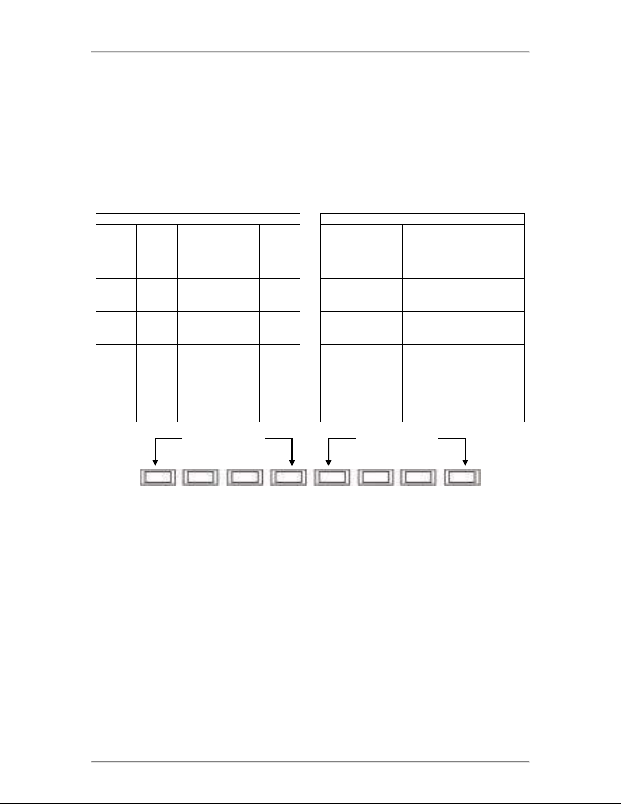
Population order
CPU1
CPU2*
1
BK00
BK10
2
BK01
BK11
3
BK02
BK12
Before You Begin
INTRODUCTION
It is important to be aware of the system considerations listed below before installing your JXT6966 or
JXTS6966 (S6966-xxx) SHB. Overall system performance may be affected by incorrect usage of these
features.
MOUSE/KEYBOARD “Y” CABLE
If you have an IOB33 I/O board in your system and you are using a “Y” cable attached to the bracket
mounted mouse/keyboard mini Din connector, be sure to use Chassis Plans’ “Y” cable, part number 5886-
000. Using a non-Chassis Plans cable may result in improper SHB operation.
DDR3-1333 MEMORY
Chassis Plans recommends ECC registered DDR3 memory modules for use on the JXT6966/JXTS6966
SHBs and these ECC registered (72-bit) DDR3 Mini-DIMMs must be PC3-10600 or PC3-8500 compliant.
Unbuffered ECC DDR3 Mini-DIMMs are also supported on the JXT boards, but you cannot mix the two
different memory types on the same SHB.
NOTES:
To maximize system performance and reliability, Chassis Plans recommends populating
each memory channel with DDR3 Mini-DIMMs with the same interface speed.
All memory modules must have gold contacts.
Low voltage (DDR3L) Mini-DIMMs are not supported.
The SHB supports the following memory module memory latency timings:
o 6-6-6 for 800MHz DDR3 Mini-DIMMs
o 7-7-7 and 8-8-8 for 1066MHz DDR3 Mini-DIMMs
o 9-9-9 for 1333MHz DDR3 Mini-DIMMs
Populating the memory sockets with Mini-DIMMs having different speeds is supported
on the SHB; however, the overall memory interface speed will run at the speed of the
slowest Mini-DIMM.
Populate the memory sockets starting with the Mini-DIMM socket closest to the CPU
and work your way toward the edges of the SHB as illustrated in the chart below:
*CPU2 is available on the JXT6966 dual-processor board version only
*Using a balanced memory population approach ensures maximum memory interface
performance. A “balance approach” means using an equal number of Mini-DMMs
for each processor on a dual-processor JXT6966 SHB whenever possible.
The memory DIMMs on the SHB connect directly to the CPU and at least one memory module must be
installed on the board. The JXTS6966 SHB versions feature one processor; however, memory sockets
BK10, BK11 and BK12 are installed on the SHB but are not active in this single-processor board version.
SATA RAID OPERATION
The Intel® 3420 Platform Controller Hub (PCH) used on the SHB features Intel® Rapid Storage
Technology (Intel® RST), which allows the PCH’s SATA controller to be configured as a RAID controller
supporting RAID 0, 1, 5 and 10 implementations. To configure the SATA ports as RAID drives or to use
advanced features of the PCH, you must install the Intel® RST driver software. A link to the software is
also located on Chassis Plans’ website by accessing the Downloads tab of the JXT6966 product detail page
or the RAID Drivers section of the Technical Support page.
iv CHASSIS PLANS
Page 9

JXT6966 / JXTS6966 Technical Reference
POWER CONNECTION
The PICMG® 1.3 specification supports soft power control signals via the Advanced Configuration and
Power Interface (ACPI). The JXT6966/JXTS6966 supports these signals, controlled by the ACPI and are
used to implement various sleep modes. When control signals are implemented, the type of ATX or EPS
power supply used and the operating system software will dictate how system power should connect to the
SHB. It is critical that the correct method be used. Refer to - Power Connection section in the JXT manual
to determine the method that will work with your specific system design. The Advanced Setup chapter in
the manual contains the ACPI BIOS settings.
PCI EXPRESS 2.0 LINKS AND PICMG® 1.3 BACKPLANES
The PCI Express® links on the JXT6966 connect directly to the processors. These links can operate as
either PCI Express 2.0 or PCI Express 1.1 links based on the end-point devices on the backplane that are
connected to the SHB. In addition to automatically configuring themselves for either PCIe 2.0 or PCIe 1.1
operations, the links also configure themselves for either graphics or server-class operations. In other
words, the multiple x4 links from the processors (links A0, A1, A2 and A3) can be combined into a single
x16 PCIe electrical link or multiple x8 links on a backplane. The CPU’s x4 links can train down to x1
links, but cannot bifurcate into multiple x1 links. The PCIe link (B0) from the board’s PCH has a x4
default configuration and can be made to bifurcate into four, x1 PCIe links with a factory modification to
the JXT board. Contact Chassis Plans if you require this B0 link configuration change. An optional
PEX10 module connected to a dual-processor JXT6966 provides more backplane links than are currently
supported in the PICMG 1.3 specification. This JXT6966 capability provides additional PCI Express
bandwidth and option card support in the system design. Refer to the PCI Express® Reference chapter and
to Appendix C - PCI Express Backplane Usage of this manual for more information.
PICMG 1.3 BACKPLANE I/O
The JXT6966 and JXTS6966 enable the following PICMG 1.3 backplane I/O connectivity via the SBC’s
edge connector C:
Four USB 2.0 interfaces
One 10/100Base-T Ethernet interface
PICMG 1.3 BACKPLANE CLASSIFICATION
The JXT6966 and JXTS6966 are system host boards that can operate as either a Server or Graphics-Class
PICMG 1.3 SHB. The JXT SHBs are essentially combo-class boards because of the capabilities of the PCI
Express links built into the SHB’s processors. Chassis Plans recommends using a combo-class PICMG 1.3
backplane such as the Chassis Plans BPC7009 or BPC7041 with the SHBs in order to ensure the use of all
available backplane option card slots. See Appendix C, PCI Express Backplane Usage for more details.
OFF-BOARD VIDEO CARD USAGE
If the system design requires an off-board video card, then the card must be placed in a backplane slot
driven with PCI Express links from the JXT6966’s first processor. This is an Aptio® 4.x BIOS limitation
that may be corrected in future software revisions. Listed below are the acceptable BPC7009 and BPC7041
backplane slots for use with an off-board video card:
BPC7009 - Card slot PCIe1, PCIe2 or PCIe3
BPC7041 - Card slot PCIe6, PCIe7, PCIe8, PCIe9 or PCIe10
BIOS
The JXT6966 and JXTS6966 feature the Aptio® 4.x BIOS from American Megatrends, Inc. (AMI) with a
ROM-resident setup utility called the Aptio Text Setup Environment or TSE. Details of the Aptio TSE are
provided in the separate JXT6966 / JXTS6966 BIOS Technical Reference manual.
FOR MORE INFORMATION
For more information on any of these features, refer to the appropriate sections JXT6966 / JXTS6966
Hardware Technical Reference Manual. The BIOS and hardware technical reference manuals are available
under the Downloads tab on the JXT6966 or JXTS6966 web pages.
CHASSIS PLANS v
Page 10

JXT6966 / JXTS6966 Technical Reference
This page intentionally left blank
vi CHASSIS PLANS
Page 11

JXT6966 / JXTS6966 Technical Reference Specifications
Model #
Model Name
Speed
Intel CPU Number
S6966-053
JXT/2.0QMR
2.0GHz
EC5509
S6966-125
JXT/2.53QN
2.53GHz
EC5549
S6966-224
JXT/2.13QM
2.13GHz
LC5528
S6966-222
JXT/1.73QM
1.73GHz
LC5518
S6966-425
JXT/2.27DNR
2.27GHz
EC5539
Chapter 1 Specifications
Introduction
The JXT6966 and JXTS6966 are combo-class, PICMG® 1.3 system host boards that support the Intel®
Xeon® C5500 processors. These CPUs feature the Nehalem micro-architecture and were developed under
the codename Jasper Forest. The processors have a DDR3 integrated memory controller that supports three
DDR3-1333 memory interface channels per processor resulting in six direct access memory interfaces on
the JXT6966 board version. The six interfaces connect to six DDR3 Mini-DIMM sockets. With 4GB
DDR3 Mini-DIMMs the total system memory capacity for a JXT6966 is 24GB and will double to 48GB
once 8GB DDR3 Mini-DIMMs come on the market. The maximum theoretical system memory capacity
for the JXT6966 is 192GB. The system memory capacities are cut in half for the single processor
JXTS6966 board version.
PCI Express 2.0/1.1 links are built into the processors and the Intel® Quick Path Interface (Intel® QPI)
between processors on the JXT6966 enables CPU resource sharing for an additional system throughput
speed boost. All of the PCI Express interface links needed for a PICMG 1.3 compliant backplane are
provided by the PCIe links out of CPU1 and the additional link out of the Intel® 3420 Platform Controller
Hub (PCH). CPU2 on the JXT6966 provides four additional x4 PCI Express 2.0 or 1.1 links to a backplane
via an optional plug-in card called the Chassis Plans PEX10. These extra links provide added bandwidth to
systems equipped with a backplane such as the Chassis Plans BPC7009 or BPC7041. An optional IOB33
module provides an extra x1 PCIe 1.1 link to a backplane equipped with a PCIe expansion slot.
Video and I/O features on the JXT boards include:
A Graphics Processing Unit (GPU) driven with an internal x1 PCIe link and capable of
supporting pixel resolutions up to 1920 x 1200 (WUXGA) with a 64k color depth
Three Gigabit Ethernet interfaces with two on the I/O plate and one available for use on a
PICMG 1.3 compliant backplane
Six SATA/300 ports that can support independent drives or RAID drive arrays
Eight USB 2.0 interfaces
The listing below summarizes the available versions of the JXT6966 and JXTS6966 system host boards.
Dual-Processor Models
Dual Intel Xeon Processors (Jasper Forest) - Quad Core, 4.8GT/s QPI, 8MB cache, No H-T*:
* H-T = Intel Hyper-Threading
Dual Intel Xeon Processors (Jasper Forest) - Quad Core, 5.86GT/s QPI, 8MB cache, With H-T:
Dual Intel Xeon Processors (Jasper Forest) - Quad Core, 4.8GT/s QPI, 8MB cache, With H-T:
Dual Intel Xeon Processors (Jasper Forest) - Dual Core, 5.86GT/s QPI, 4MB cache, No H-T:
1-1 CHASSIS PLANS
Page 12

Specifications JXT6966 / JXTS6966 Technical Reference
Model #
Model Name
Speed
Intel CPU Number
S6966-093
JXTS/2.0QMR
2.0GHz
EC5509
S6966-165
JXTS/2.53QN
2.53GHz
EC5549
S6966-264
JXTS/2.13QM
2.13GHz
LC5528
S6966-262
JXTS/1.73QM
1.73GHz
LC5518
S6966-465
JXTS/2.27DNR
2.27GHz
EC5539
Single-Processor Models
Single Intel Xeon Processor (Jasper Forest) - Quad Core, 4.8GT/s QPI, 8MB cache, No H-T*:
* H-T = Intel Hyper-Threading
Single Intel Xeon Processor (Jasper Forest) - Quad Core, 5.86GT/s QPI, 8MB cache, With H-T:
Single Intel Xeon Processor (Jasper Forest) - Quad Core, 4.8GT/s QPI, 8MB cache, With H-T:
Single Intel Xeon Processor (Jasper Forest) - Dual Core, 5.86GT/s QPI, 4MB cache, No H-T:
Features
Intel® Xeon® C5500 Processors (Jasper Forest)
Intel® 3420 Platform Controller Hub
Direct PCI Express® 2.0 links into the Intel® Xeon® C5500 Processors
A Combo-class SHB that is compatible with PCI Industrial Computer Manufacturers Group
(PICMG) 1.3 Specifiction
Direct PCI Express® 2.0 links into the Intel® Xeon® C5500 Processors
JXT6966 provides a total of 37 lanes of PCI Express for off-board system integration
Direct DDR3-1333 Memory Interfaces into the Intel® Xeon® C5500 Processors
Six DDR3 Mini-DIMM sockets capable of supporting up to 192GB of system memory on a dual-
processor JXT6966, 24GB maximum capacity with readily available 4GB DDR3 Mini-DIMMs
Video interface utilizing XGI® Volari™ Z11M Graphice Processing Unit
Two 10/100/1000Base-T Ethernet interfaces available on the SHB’s I/O plate
Six Serial on-board ATA/300 ports support four independent SATA storage devices
SATA/300 ports may be configured to support RAID 0, 1, 5 or 10 implementations
Eight Universal Serial Bus (USB 2.0) interfaces
Off-board I/O support provided for one 10/100Base-T Ethernet interface and four USB 2.0 port
connections on a PICMG 1.3 backplane
Legacy I/O, dual serial port and x1 PCIe link expansion available via Chassis Plans IOB33
expansion board
An additional 16 PCI Express 2.0 lanes are available when using an optional PEX10 board on a
JXT6966 connected to a Chassis Plans BPC7009 or BPC7041 PICMG 1.3 backplane
Full-length stiffner bars on the rear of the SHB enhances the rugged nature on the board by
maximizing component protection and simplifying mechanical system integration
Full PC compatibility
CHASSIS PLANS 1-2
Page 13

JXT6966 / JXTS6966 Technical Reference Specifications
JXT6966 (S6966-xxx) – Dual-Processor SHB Block Diagram
1-3 CHASSIS PLANS
Page 14

Specifications JXT6966 / JXTS6966 Technical Reference
JXT6966 (S6966-xxx) – Dual-Processor SHB Layout Diagram
CHASSIS PLANS 1-4
Page 15

JXT6966 / JXTS6966 Technical Reference Specifications
JXTS6966 (S6966-xxx) – Single-Processor SHB Block Diagram
1-5 CHASSIS PLANS
Page 16

Specifications JXT6966 / JXTS6966 Technical Reference
JXTS6966 (S6966-xxx) – Single-Processor SHB Layout Diagram
CHASSIS PLANS 1-6
Page 17

JXT6966 / JXTS6966 Technical Reference Specifications
Processor
Intel® Xeon® C5500 Series Processor – Nehalem-EP micro-architecture (Jasper Forest)r
Processor plugs into an LGA1366 socket
Serial Interconnect Interface
PCI Express® 2.0 and 1.1 compatible
Data Path
DDR3-1333 Memory - 72-bit (per channel)
Serial Interconnect Speeds
PCI Express 2.0 – 5.0GHz per lane
PCI Express 1.1 - 2.5GHz per lane
Intel® Quick Path Interconnect Supported Speeds Between CPUs
The Intel® 3420 PCH supports 4.8GT/s or 5.86GT/s between processors. The speed of the Intel® QPI
depends on the type of CPU installed. The Quick Path Interconnect enables both processor-to-processor
resource sharing and fast data transfers between CPUs and the Intel® 3420 PCH.
Intel® Direct Media Interface (DMI)Speed Between Processor and Intel® 3420 PCH
This full duplex interface operates at 10Gb/s in each direction and provides data communications between
the PCH and processor. On a dual-processor, JXT6966 the first CPU connects to the PCH and the second
CPU feeds its information to the PCH via the first CPU’s DMI link.
Memory Interface
Three DDR3-1333MHz memory channels per processor; peak memory interface bandwidth is 32GB/s
when using PC3-10600 Mini-DIMMs.
DMA Channels
The SHB is fully PC compatible with seven DMA channels, each supporting type F transfers.
Interrupts
The SHB is fully PC compatible with interrupt steering for PCI plug and play compatibility.
Bios (Flash)
The JXT boards use an Aptio® 4.x BIOS from American Megatrends Inc. (AMI). The BIOS features builtin advanced CMOS setup for system parameters, peripheral management for configuring on-board
peripherals and other system parameters. The BIOS resides in a 32Mb Atmel® AT25DF321SU SPI Serial
EEPROM (SPI Flash). The BIOS may be upgraded from a USB thumb drive storage device by pressing
<Ctrl> + <Home> immediately after reset or power-up with the USB device installed in drive A:. Custom
BIOSs are available.
Cache Memory
The processors include either a 4MB or 8MB last-level cache (LLC) memory capacity that is equally
shared between all of the processor cores on the die.
1-7 CHASSIS PLANS
Page 18

Specifications JXT6966 / JXTS6966 Technical Reference
Population order
CPU1
CPU2*
1
BK00
BK10
2
BK01
BK11
3
BK02
BK12
DDR3-1333 Memory
Each processor on the SHB supports three separate DDR3-1333 memory interfaces. There are six active
Mini-DIMM sockets on the JXT6966 models and each one can support up to 32GB DIMMs for a total
possible DDR3 system memory capacity of 192GB. The single processor models support three active Mini-
DIMM sockets and each socket can support up to 32GB DIMMs for a total possible DDR3 system memory capacity of
96GB on a JXTS6966. However, currently available DDR3 Mini-DIMM memory capacities of 2GB, 4GB
and 8GB are more common in today’s market; thereby, making the maximum practical limit of system
memory supported 48GB on dual-processor SHBs and 24GB on single processor models. The peak
memory interface bandwidth per channel is 32/GB/s when using PC3-10600 (i.e. DDR3-1333) MiniDIMMs. Each of the direct CPU memory channel (BK##) terminates with a single in-line Mini-DIMM
memory module socket. The System BIOS automatically detects memory type, size and speed.
Chassis Plans recommends ECC registered DDR3 memory modules for use on the JXT6966/JXTS6966
SHBs and these ECC registered (72-bit) DDR3 Mini-DIMMs must be PC3-10600 or PC3-8500 compliant.
Unbuffered ECC DDR3 Mini-DIMMs are also supported on the JXT boards, but you cannot mix the two
different memory types on the same SHB.
NOTES:
To maximize system performance and reliability, Chassis Plans recommends populating
each memory channel with DDR3 Mini-DIMMs with the same interface speed.
All memory modules must have gold contacts.
Low voltage (DDR3L) Mini-DIMMs are not supported.
The SHB supports the following memory module memory latency timings:
o 6-6-6 for 800MHz DDR3 Mini-DIMMs
o 7-7-7 and 8-8-8 for 1066MHz DDR3 Mini-DIMMs
o 9-9-9 for 1333MHz DDR3 Mini-DIMMs
Populating the memory sockets with Mini-DIMMs having different speeds is supported
on the SHB; however, the overall memory interface speed will run at the speed of the
slowest Mini-DIMM.
Populate the memory sockets starting with the Mini-DIMM socket closest to the CPU
and work your way toward the edges of the SHB as illustrated in the chart below:
*CPU2 is available on the JXT6966 dual-processor board version only
The memory DIMMs on the SHB connect directly to the CPU and at least one memory module must be
installed on the board. The JXTS6966 SHB versions feature one processor; however, memory slots BK10,
BK11 and BK12 are installed on the SHB but are not active in this single-processor board version.
Universal Serial Bus (USB)
The SHB support eight high-speed USB 2.0 ports. Connectors for two of the USB ports (0 and 1) are on the
I/O bracket and USB ports 2 and 3 are available via headers on the SHB. USB ports 4, 5, 6 and 7 are
routed directly to edge connector C of the SHB for use on a PICMG 1.3 backplane.
Video Interface
The SHB features a Graphics Processing Unit (GPU) with 8MB of video memory, and the GPU is driven
by a x1 PCIe link from the SHB’s Intel® 3420 PCH. This combination of features enables the SHB’s
video port; located on the board’s I/O plate, to support pixel resolutions up to 1920 x 1200 (WUXGA) with
a 64k color depth.
CHASSIS PLANS 1-8
Page 19

JXT6966 / JXTS6966 Technical Reference Specifications
PCI Express Interfaces
The PCI Express® links on the JXT6966 connect directly to the processors. These links can operate as
either PCI Express 2.0 or PCI Express 1.1 links based on the end-point devices on the backplane that are
connected to the SHB. In addition to automatically configuring themselves for either PCIe 2.0 or PCIe 1.1
operations, the links also configure themselves for either graphics or server-class operations. In other
words, the multiple x4 links from the processors (links A0, A1, A2 and A3) can be combined into a single
x16 PCIe electrical link or multiple x8 links on a backplane. The CPU’s x4 links can train down to x1
links, but cannot bifurcate into multiple x1 links. The PCIe link (B0) from the board’s PCH has a x4
default configuration and can be made to bifurcate into four, x1 PCIe links with a factory modification to
the JXT board. Contact Chassis Plans if you require this B0 link configuration change. An optional
PEX10 module connected to a dual-processor JXT6966 provides more backplane links than are currently
supported in the PICMG 1.3 specification. This JXT6966 capability provides additional PCI Express
bandwidth and option card support in the system design. The single processor JXTS6966 supports the
PICMG 1.3 PCI Express specification. The single processor on the JXTS6966 configures the PCIe links
for either server or graphics-class link operations based on the backplane type and the end-point devices on
the backplane. The JXTS6966 does not support the optional PEX10 link expansion module, but both SHB
models support the optional IOB33 and the IOB’s x1 PCI Express expansion link down to a backplane with
a PCIe Expansion slot. Refer to the PCI Express® Reference chapter and to Appendix C - PCI Express
Backplane Usage of this manual for more information.
Ethernet Interfaces
The JXT6966/JXTS6966 SHBs support three Ethernet interfaces. The first two interfaces are on-board
10/100/1000Base-T Ethernet interfaces located on the board's I/O bracket and implemented using an Intel®
82575EB Gigabit Ethernet Controller. These I/O bracket interfaces support Gigabit, 10Base-T and
100Base-TX Fast Ethernet modes and are compliant with the IEEE 802.3 Specification.
The main components of the I/O bracket Ethernet interfaces are:
Intel® 82575EB for 10/100/1000-Mb/s media access control (MAC) with SYM, a serial ROM port
and a PCIe interface
Serial ROM for storing the Ethernet address and the interface configuration and control data
Integrated RJ-45/Magnetics module connectors on the SHB's I/O bracket for direct connection to
the network. The connectors require category 5 (CAT5) unshielded twisted-pair (UTP) 2-pair
cables for a 100-Mb/s network connection or category3 (CAT3) or higher UTP 2-pair cables for a
10-Mb/s network connection. Category 5e (CAT5e) or higher UTP 2-pair cables are recommended
for a 1000-Mb/s (Gigabit) network connection.
Link status and activity LEDs on the I/O bracket for status indication (See Ethernet LEDs and
Connectors later in this chapter.)
The third LAN is supported by the Intel® 3420 and the Intel® 82578 Gigabit Ethernet PHY. This
10/100/1000Base-T Ethernet interface is routed to the PICMG 1.3 backplane via edge connector C of the
SHB.
Software drivers are supplied for most popular operating systems.
Serial ATA/300 Ports
The six Serial ATA (SATA) ports on the SHB are driven with a built-in SATA controller from the Intel®
3420 Platform Controller Hub (PCH). The board’s SATA/300 interfaces comply with the SATA 1.0
specification and can support six independent SATA storage devices such as hard disks and CD-RW
devices at data transfer rates up to 300MB per second on each port. The SATA controller has two BIOS
selectable modes of operation with a legacy (i.e. IDE) mode using I/O space, and an AHCI mode using
memory space. Software that uses legacy mode will not have AHCI capabilities. The board’s PCH
features Intel® Rapid Storage Technology, which allows a third BIOS-selectable SATA controller
configuration that enables a RAID configuration capable of supporting RAID 0, 1, 5 and 10 storage array
implementations.
1-9 CHASSIS PLANS
Page 20

Specifications JXT6966 / JXTS6966 Technical Reference
Monitored Voltage
Nominal Low Limit
Voltage Source
+5V
+3.3V
Vcc_DDR(+1.5V)
Vtt_CPU(1.2V)
+1.05V(Chipset)
+1.80V(Chipset)
4.75 volts
2.97 volts
1.15 volts
0.85 volt
0.945 volt
1.62 volts
System Power Supply
System Power Supply
On-Board Regulator
On-Board Regulator
On-Board Regulator
On-Board Regulator
Processor Type
SHB Type
Processor
Speed
+5V
+12V
+3.3V
CPU Idle State:
Intel Xeon C5500
Quad-Core (EC5549)
JXT6966
(Dual CPU)
2.53GHz
1.07A
6.48A
4.44A
Intel Xeon C5500
Quad-Core (EC5549)
JXTS6966
(Single CPU)
2.53GHz
0.71A
3.28A
2.10A
Intel Xeon C5500
Dual-Core (EC5539)
JXT6966
(Dual CPU)
2.27GHz
0.90A
6.29A
4.48A
Intel Xeon C5500
Dual-Core (EC5539)
JXTS6966
(Single CPU)
2.27GHz
0.71A
3.02A
2.08A
Intel Xeon C5500
Quad-Core (EC5509)
JXT6966
(Dual CPU)
2.00GHz
0.90A
5.96A
4.91A
Intel Xeon LV C5500
Quad-Core (LC5528)
JXT6966
(Dual CPU)
2.13GHz
1.06A
4.87A
4.91A
Intel Xeon LV C5500
Quad-Core (LC5528)
JXTS6966
(Single CPU)
2.13GHz
0.71A
2.90A
2.06A
100% CPU Stress State:
Intel Xeon C5500
Quad-Core (EC5549)
JXT6966
(Dual CPU)
2.53GHz
1.09A
12.20A
4.48A
Intel Xeon C5500
Quad-Core (EC5549)
JXTS6966
(Single CPU)
2.53GHz
0.72A
7.99A
2.12A
Intel Xeon C5500
Dual-Core (EC5539)
JXT6966
(Dual CPU)
2.27GHz
0.92A
9.78A
4.48A
Intel Xeon C5500
Dual-Core (EC5539)
JXTS6966
(Single CPU)
2.27GHz
0.72A
5.15A
2.09A
Intel Xeon C5500
Quad-Core (EC5509)
JXT6966
(Dual CPU)
2.00GHz
0.90A
10.39A
4.93A
Intel Xeon LV C5500
Quad-Core (LC5528)
JXT6966
(Dual CPU)
2.13GHz
1.06A
10.57A
4.94A
Intel Xeon LV C5500
Quad-Core (LC5528)
JXTS6966
(Single CPU)
2.13GHz
0.72A
6.33A
2.07A
Power Fail Detection
A hardware reset is issued when any of the monitored voltages drops below its specified nominal low
voltage limit. The monitored voltages and their nominal low limits are listed below.
Battery
A built-in lithium battery is provided, for ten years of data retention for CMOS memory.
CAUTION: There is a danger of explosion if the battery is incorrectly replaced. Replace it only with the
same or equivalent type recommended by the manufacturer. Dispose of used batteries according to the
manufacturer's instructions.
Power Requirements
The following are nominal values with 12GB and 6GB of system memory installed*.
Tolerance for all voltages is +/- 5%
*12GB (6, 2GB DDR3 Mini-DIMMs) for a dual-processor JXT6966 and 6GB (3, 2GB DDR3 MiniDIMMs) for a single-processor JXTS6966
CHASSIS PLANS 1-10
Page 21

JXT6966 / JXTS6966 Technical Reference Specifications
CAUTION: Chassis Plans recommends an EPS type of power supply for systems using high-performance
processors. The power needs of backplane option cards, high-performance processors and other system
components may result in drawing 20A of current from the +12V power supply line. If this occurs,
hazardous energy (240VA) could exist inside the system chassis. Final system/equipment suppliers must
provide protection to service personnel from these potentially hazardous energy levels.
Stand-by voltages may be used in the final system design to enable certain system recovery operations. In
this case, the power supply may not completely remove power to the system host board when the power
switch is turned off. Caution must be taken to ensure that incoming system power is completely
disconnected before removing the system host board.
Temperature/Environment
Operating Temperature: 0º C. to 50º C.
Air Flow Requirement: 350LFM continuous airflow
Storage Temperature: - 40º C. to 70º C.
Humidity: 5% to 90% non-condensing
Mechanical
The standard cooling solution used on the JXT6966 and JXTS6966 SHBs enables placement of option
cards approximately 2.75” (69.85mm) away from the top component side of the SHB. Contact Chassis
Plans for a system engineering consultation if your application needs a lower profile cooling solution. The
SHB’s overall dimensions are 13.330” (33.858cm) L x 4.976” (12.639cm) H. The relative PICMG 1.3
SHB height off the backplane is the same as a PICMG 1.0 SBC due to the shorter PCI Express backplane
connectors.
Board Stiffener Bars
The two stiffener bars located on the back of the SHB maximize system integrity by ensuring proper SHB
alignment within the card guides of a computer chassis. The stiffeners provide reliable SHB operation by
protecting sensitive board components from mechanical damage and assist in the safe insertion and
removal of the SHB from the system.
UL Recognition
This SHB is a UL recognized product listed in file #E208896 when integrated into an industrial computer
such as the Chassis Plans C5000. This board was investigated and determined to be in compliance under
the Bi-National Standard for Information Technology Equipment. This included the Electrical Business
Equipment, UL 1950, Third Edition, and CAN/CSA C22.22 No. 950-95.
1-11 CHASSIS PLANS
Page 22

Specifications JXT6966 / JXTS6966 Technical Reference
Jumper
Description
JU1
SPI Update (two position jumper)
I
nstall for one power-up cycle to enable the board to unprotect the SHB’s SPI storage
device.
Remove for normal operation. *
CAUTION: Installing this jumper is only done for special board operations such as
changing the PCI Express link bifurcation operation. Contact Chassis Plans tech
support before installing this jumper to prevent any unintended system operation.
JU8
Password Clear (two position jumper)
Install for one power-up cycle to reset the password to the default (null password).
Remove for normal operation. *
JU12
CMOS Clear (three position jumper)
Install on the LEFT to clear.
Install on the RIGHT to operate. *
NOTE: To clear the CMOS, power down the system and install the jumper on the
TOP. Wait for at least two seconds, move the jumper back to the BOTTOM and turn
the power on. When AMIBIOS displays the "CMOS Settings Wrong" message, press
F1 to go into the BIOS Setup Utility, where you may reenter your desired BIOS
settings, load optimal defaults or load failsafe defaults.
Configuration Jumpers
The setup of the configuration jumpers on the SHB is described below. * indicates the default value of each
jumper.
NOTE: For the three-position JU12 jumper, "RIGHT" is toward the I/O bracket side of the board; "LEFT"
is toward the CPU1 DDR3 Memory sockets.
CHASSIS PLANS 1-12
Page 23

JXT6966 / JXTS6966 Technical Reference Specifications
LED/Connector
Description
Activity LED
Green LED which indicates network activity. This is the upper LED on the
LAN connector (i.e., toward the upper memory sockets).
Off
Indicates there is no current network transmit or receive activity.
On (flashing)
Indicates network transmit or receive activity.
Speed LED
Green LED which identifies the connection speed. This is the lower LED on
the LAN connector (i.e., toward the edge connectors).
Off
Indicates a valid link at 1000-Mb/s.
Green
Indicates a valid link at 100-Mb/s.
RJ-45 Network
Connector
The RJ-45 network connector requires a category 5 (CAT5) unshielded
twisted-pair (UTP) 2-pair cable for a 100-Mb/s network connection or a
category 3 (CAT3) or higher UTP 2-pair cable for a 10-Mb/s network
connection. A category 5e (CAT5e) or higher UTP 2-pair cable is
recommended for a 1000-Mb/s (Gigabit) network connection
LED Status
Description
Off
Indicates the processor or processors are operating within acceptable
thermal levels
On (flashing)
Indicates the CPU is throttling down to a lower operating speed due to rising
CPU temperature
On (solid)
Indicates the CPU has reached the thermal shutdown threshold limit. The
SHB may or may not be operating, but a thermal shutdown may soon occur.
P4A/P4B Ethernet LEDs and Connectors
The I/O bracket houses the two RJ-45 network connectors for Ethernet LAN1and LAN2. Each LAN
interface connector has two LEDs that indicate activity status and Ethernet connection speed. Listed below
are the possible LED conditions and status indications for each LAN connector:
Status LEDs
Thermal Trip LED – LED9
The thermal trip LED indicates when a processor reaches a shut down state. The LED is located just above
the BK02 DIMM socket. LED9 indicates the processor shutdown status and thermal conditions as
illustrated below:
NOTE: When a thermal shutdown occurs, the LED will stay on in systems using non- ATX/EPS power
supplies. The CPU will cease functioning, but power will still be applied to the SHB. In systems with
ATX/EPS power supplies, the LED will turn off when a thermal shutdown occurs because system power is
removed via the ACPI soft control power signal S5. In this case, all SHB LEDs will turn off; however,
stand-by power will still be present.
1-13 CHASSIS PLANS
Page 24
Specifications JXT6966 / JXTS6966 Technical Reference
Upper Nibble (UN)
Lower Nibble (LN)
Hex.
Value
LED7
LED6
LED5
LED4
Hex.
Value
LED3
LED2
LED1
LED0
0
Off
Off
Off
Off
0
Off
Off
Off
Off 1 Off
Off
Off
On
1
Off
Off
Off
On 2 Off
Off
On
Off
2
Off
Off
On
Off
3
Off
Off
On
On 3
Off
Off
On
On 4 Off
On
Off
Off 4
Off
On
Off
Off
5
Off
On
Off
On 5
Off
On
Off
On 6 Off
On
On
Off 6
Off
On
On
Off
7
Off
On
On
On 7
Off
On
On
On 8 On
Off
Off
Off 8
On
Off
Off
Off 9 On
Off
Off
On 9
On
Off
Off
On
A
On
Off
On
Off A
On
Off
On
Off B On
Off
On
On B
On
Off
On
On C On
On
Off
Off C
On
On
Off
Off
D
On
On
Off
On D
On
On
Off
On E On
On
On
Off E
On
On
On
Off F On
On
On
On F
On
On
On
On
Lower Nibble
7 6 5 4 3 2 1 0
Upper Nibble
JXT6966 & JXTS6966 POST Code LEDs
Post Code LEDs 0 - 7
As the POST (Power On Self Test) routines are performed during boot-up, test codes are displayed on Port
80 POST code LEDs 0, 1, 2, 3, 4, 5, 6 and 7. These LED are located on the top of the SHB, just above the
board’s battery socket. The POST Code LEDs and are numbered from right (position 1 = LED0) to left
(position 8 – LED7). Refer to the board layout diagram for the exact location of the POST code LEDs.
These POST codes may be helpful as a diagnostic tool. After a normal POST sequence the LEDs are off
(00h) indicating that the SHB’s BIOS has passed control over to the operating system loader typically at
interrupt INT19h. Specific test codes and their meaning along with the following chart are listed in
Appendix A and can be used to interpret the LEDs into hexadecimal format during POST.
System BIOS Setup Utility
The JXT6966 and JXTS6966 feature the Aptio® 4.x BIOS from American Megatrends, Inc. (AMI) with a
ROM-resident setup utility called the Aptio Text Setup Environment or TSE. The TSE setup utility allows
you to select to the following categories of options:
Main Menu
Advanced Setup
Boot Setup
Security Setup
Chipset Setup
Exit
Each of these options allows you to review and/or change various setup features of your system. Details of
the Aptio TSE are provided in the separate JXT6966 / JXTS6966 BIOS Technical Reference manual. The
BIOS and hardware technical reference manuals are available under the Downloads tab on the JXT6966 or
JXTS6966 web pages.
CHASSIS PLANS 1-14
Page 25

JXT6966 / JXTS6966 Technical Reference Specifications
P1 - Video Interface Connector
15 pin connector, Kycon K31X-E15S-N
Pin
Signal
Pin
Signal
Pin
Signal
6
Gnd 1 Red
11
NC
7
Gnd
2
Green
12
EEDI
8
Gnd
3
Blue
13
HSYNC
9
+5
4
NC
14
VSYNC
10
Gnd 5 Gnd
15
EECS
P2,
P19
-
CPU Fan Power Connectors
3 pin single row header, Molex #22-23-2031
Pin
Signal
1
Gnd
2
+12V
3
FanTach
P4A,
P4B
-
10/100/1000Base-T Ethernet Connectors - LAN1/LAN2
Dual RJ-45 connector, Pulse #JG0-0024NL
Each individual RJ-45 connector is defined as follows:
Pin
Signal
Pin
Signal
1A
L2_MDI0n
1B
L1_MDI0n
2A
L2_MDI0p
2B
L1_MDI0p
3A
L2_MDI1n
3B
L1_MDI1n
4A
L2_MDI1p
4B
L1_MDI1p
5A
L2_MDI2n
5B
L1_MDI2n
6A
L2_MDI2p
6B
L1_MDI2p
7A
L2_MDI3n
7B
L1_MDI3n
8A
L2_MDI3p
8B
L1_MDI3p
9A
VCC_1.8V
9B
VCC_1.8V
10A
GND_A
10B
GND_b
P5 - Speaker Port Connector
4 pin single row header, Amp #640456-4
Pin
Signal
1
Speaker Data
2
Key
3
Gnd
4
+5V
Connectors
NOTE: Pin 1 on the connectors is indicated by the square pad on the PCB.
Note:
1 – Connector supports standard DB15 video cables
Notes:
1 – P2 is the fan connector of CPU2 and P19 is for CPU1
Notes:
1 - LAN ports support standard CAT5 Ethernet cables
2 – P4A is LAN1 and P4B is LAN1
1-15 CHASSIS PLANS
Page 26

Specifications JXT6966 / JXTS6966 Technical Reference
Connectors (Continued)
P6 - Reset Connector
2 pin single row header, Amp #640456-2
Pin
Signal
Pin
Signal
1
Gnd 2 Reset In
P12 - Hard Drive LED Connector
4 pin single row header, Amp #640456-4
Pin
Signal
1
LED+
2
LED-
3
LED-
4
LED+
P17 - Dual Universal Serial Bus (USB) Connector
10 pin dual row header, Molex #702-46-1001
(+5V fused with self-resetting fuses)
Pin
Signal
Pin
Signal
1
+5V-USB2
2
+5V-USB3
3
USB2-
4
USB3-
5
USB2+
6
USB3+
7
Gnd-USB2
8
Gnd-USB3
9
NC
10
NC
P17A
-
Universal Serial Bus (USB) Connector
USB vertical connector, Molex #6739-8001
(+5V fused with self-resetting fuse)
Pin
Signal
1
+5V-USB0
2
USB0-
3
USB0+
4
Gnd-USB0
P17B
-
Universal Serial Bus (USB) Connector
USB vertical connector, Molex #6739-8001
(+5V fused with self-resetting fuse)
Pin
Signal
1
+5V-USB1
2
USB1-
3
USB1+
4
Gnd-USB1
CHASSIS PLANS 1-16
Page 27

JXT6966 / JXTS6966 Technical Reference Specifications
Connectors (Continued)
P27,
P28,
P31,
P32,
P35,
P36
-
SATA II 300 Ports
7 pin vertical connector, Molex #67491-0031
Pin
Signal
1
Gnd 2 TX+
3
TX-
4
Gnd
5
RX-
6
RX+
7
Gnd
P21 - Power Good LED Connector
2 pin single row header, Amp #640456-2
Pin
Signal
Pin
Signal
1
LED-
2
LED+
Notes:
1 – P27 = SATA0 interface, P28 = SATA1 interface,
P31 = SATA2 interface, P32 = SATA3 interface,
P35 = SATA4 interface, P36 = SATA5 interface
2 – SATA connectors support standard SATA II interface cables
1-17 CHASSIS PLANS
Page 28

Specifications JXT6966 / JXTS6966 Technical Reference
Connectors (Continued)
P20 - I/O Expansion Mezzanine Card Connector
76 pin controlled impedance connector, Samtec #MIS-038-01-FD-K
Pin
Signal
Pin
Signal
1
+12 2 +5V_STANDBY
3
HDA_SDIN2
4
+5V_STANDBY
5
HDA_SDIN1
6
+5V_DUAL
7
HDA_SDIN0
8
+5V_DUAL
9
HDA_SYNC
10
HDA_BITCLK
11
HDA_SDOUT
12
HDA_ACRST
13
ICH_SMI#
14
ICH_RCIN#
15
ICH_SIOPME#
16
ICH_A20GATE
17
Gnd
18
Gnd
19
L_FRAME#
20
L_AD3
21
L_DRQ1#
22
L_AD2
23
L_DRQ0#
24
L_AD1
25
SERIRQ
26
L_AD0
27
Gnd
28
Gnd
29
PCLK14SIO
30
PCLK33LPC
31
Gnd
32
Gnd
33
SMBDATA_RESUME
34
IPMB_DAT
35
SBMCLK_RESUME
36
IPMB_CLK
37
SALRT#_RESUME
38
IPMB_ALRT#
39
Gnd
40
Gnd
41
EXP_CLK100
42
EXP_RESET#
43
EXP_CLK100#
44
ICH_WAKE#
45
Gnd
46
Gnd
47
C_PE_TXP5
48
C_PE_RXP5
49
C_PE_TXN5
50
C_PE_RXN5
51
Gnd
52
Gnd
53
NC
54
NC
55
NC
56
NC
57
Gnd
58
Gnd
59
NC
60
NC
61
NC
62
NC
63
Gnd
64
Gnd
65
NC
66
NC
67
NC
68
NC
69
Gnd
70
Gnd
71
+3.3V
72
+5V
73
+3.3V
74
+5V
75
+3.3V
76
+5V
CHASSIS PLANS 1-18
Page 29

JXT6966 / JXTS6966 Technical Reference Specifications
Connectors (Continued)
P3 - PCI Express Gen 2.0 Expansion Connector
(For PEX10 option module)
80 pin (40 differential pairs) high-speed socket strip, Samtec #QSH-040-01-F-D-DP
Pin
Signal
Pin
Signal
1
P1_PE_TXP0
2
P1_PE_RXP0
3
P1_PE_TXN0
4
P1_PE_RXN0
5
P1_PE_TXP1
6
P1_PE_RXP1
7
P1_PE_TXN1
8
P1_PE_RXN1
9
P1_PE_TXP2
10
P1_PE_RXP2
11
P1_PE_TXN2
12
P1_PE_RXN2
13
P1_PE_TXP3
14
P1_PE_RXP3
15
P1_PE_TXN3
16
P1_PE_RXN3
17
P1_PE_TXP4
18
P1_PE_RXP4
19
P1_PE_TXN4
20
P1_PE_RXN4
21
P1_PE_TXP5
22
P1_PE_RXP5
23
P1_PE_TXN5
24
P1_PE_RXN5
25
P1_PE_TXP6
26
P1_PE_RXP6
27
P1_PE_TXN6
28
P1_PE_RXN6
29
P1_PE_TXP7
30
P1_PE_RXP7
31
P1_PE_TXN7
32
P1_PE_RXN7
33
P1_PE_CFG0
34
P1_GEN2_DSBL#
35
P1_PE_CGF1
36
P1_PE_CFG2
37
NC
38
NC
39
NC
40
NC
41
P1_PE_TXP8
42
P1_PE_RXP8
43
P1_PE_TXN8
44
P1_PE_RXN8
45
P1_PE_TXP9
46
P1_PE_RXP9
47
P1_PE_TXN9
48
P1_PE_RXN9
49
P1_PE_TXP10
50
P1_PE_RXP10
51
P1_PE_TXN10
52
P1_PE_RXN10
53
P1_PE_TXP11
54
P1_PE_RXP11
55
P1_PE_TXN11
56
P1_PE_RXN11
57
P1_PE_TXP12
58
P1_PE_RXP12
59
P1_PE_TXN12
60
P1_PE_RXN12
61
P1_PE_TXP13
62
P1_PE_RXP13
63
P1_PE_TXN13
64
P1_PE_RXN13
65
P1_PE_TXP14
66
P1_PE_RXP14
67
P1_PE_TXN14
68
P1_PE_RXN14
69
P1_PE_TXP15
70
P1_PE_RXP15
71
P1_PE_TXN15
72
P1_PE_RXN15
73
NC
74
NC
75
NC
76
NC
77
NC
78
NC
79
NC
80
NC
Note:
1 – Need CPU2 installed for PCIe GEN 2.0 link expansion via the Chassis Plans PEX10
option
module.
1-19 CHASSIS PLANS
Page 30

Specifications JXT6966 / JXTS6966 Technical Reference
This page intentionally left blank
CHASSIS PLANS 1-20
Page 31

JXT6966 / JXTS6966 Technical Reference PCI Express Reference
Chapter 2 PCI Express® Reference
Introduction
PCI Express® is a high-speed, high-bandwidth interface with multiple channels (lanes) bundled together
with each lane using full-duplex, serial data transfers with high clock frequencies.
The PCI Express architecture is based on the conventional PCI addressing model, but improves upon it by
providing a high-performance physical interface and enhanced capabilities. Whereas the PCI bus
architecture provided parallel communication between a processor board and backplane, the PCI Express
protocol provides high-speed serial data transfer, which allows for higher clock speeds. The same data rate
is available in both directions simultaneously, effectively reducing bottlenecks between the system host
board (SHB) and PCI Express option cards.
PCI Express option cards may require updated device drivers. Most operating systems that support legacy
PCI cards will also support PCI Express cards without modification. Because of this design, PCI, PCI-X
and PCI Express option cards can co-exist in the same system.
PCI Express connectors have lower pin counts than PCI bus connectors. The PCIe connectors are
physically different, based on the number of lanes in the connector.
PCI Express Links
Several PCI Express channels (lanes) can be bundled for each expansion slot, leaving room for stages of
expansion. A link is a collection of one or more PCIe lanes. A basic full-duplex link consists of two
dedicated lanes for receiving data and two dedicated lanes for transmitting data. PCI Express supports
scalable link widths in 1-, 4-, 8- and 16-lane configurations, generally referred to as x1, x4, x8 and x16
slots. A x1 slot indicates that the slot has one PCIe lane, which gives it a bandwidth of 250MB/s in each
direction. Since devices do not compete for bandwidth, the effective bandwidth, counting bandwidth in
both directions, is 500MB/s (full-duplex).
The number and configuration of an SHB’s PCI Express links is determined by specific component PCI
Express specifications. In PCI Express Gen 1 the bandwidths for the PCIe links are determined by the link
width multiplied by 250MB/s and 500MB/s, as follows:
Slot Full-Duplex
Size Bandwidth Bandwidth
x1 250MB/s 500MB/s
x4 1GB/s 2GB/s
x8 2GB/s 4GB/s
x16 4GB/s 8GB/s
In PCI Express Gen 2 the bandwidths for the PCIe links are doubled as compared to PCIe Gen 1.1 as
shown below:
Slot Full-Duplex
Size Bandwidth Bandwidth
x1 500MB/s 1GB/s
x4 2GB/s 4GB/s
x8 4GB/s 8GB/s
x16 8GB/s 16GB/s
2-1 CHASSIS PLANS
Page 32

PCI Express Reference JXT6966 / JXTS6966 Technical Reference
Scalability is a core feature of PCI Express. Some chipsets allow a PCI Express link to be subdivided into
additional links, e.g., a x8 link may be able to be divided into two x4 links. In addition, although a board
with a higher number of lanes will not function in a slot with a lower number of lanes (e.g., a x16 board in
a x1 slot) because the connectors are mechanically and electrically incompatible, the reverse configuration
will function. A board with a lower number of lanes can be placed into a slot with a higher number of lanes
(e.g., a x4 board into a x16 slot). The link auto-negotiates between the PCI Express devices to establish
communication. The mechanical option card slots on a PICMG 1.3 backplane must have PCI Express
configuration straps that alert the SHB to the PCI Express electrical configuration expected. The SHB can
then reconfigure the PCIe links for optimum system performance.
For more information, refer to the PCI Industrial Manufacturers Group’s SHB Express® System Host
Board PCI Express Specification, PICMG® 1.3.
SHB Configurations
The JXT6966 and JXTS6966 are combo class SHBs that support either PCI Express server-class or
graphics-class backplane configurations. Server applications require multiple, high-bandwidth PCIe links,
and therefore the server-class SHB/backplane configuration is identified by multiple x8 and x4 links to the
SHB edge connectors.
SHBs which require high-end video or graphics cards generally use a x16 PCI Express link. The graphicsclass SHB/backplane configuration is identified by one x16 PCIe link and one x4 or four x1 links to the
edge connectors. As PCI Express chipsets continue to evolve, it is possible that more x4 and/or x1 links
could be supported in graphics-class SHBs. Currently, most video or graphics cards communicate to the
SHB at an effective x1, x4 or x8 PCI Express data rate and do not actually make use of all of the signal
lanes in a x16 connector.
NOTE: The JXT6966 / JXTS6966 eliminates the PICMG 1.3 requirement that server-class SHBs should
always be used with server-class PICMG 1.3 backplanes and graphics-class SHBs should always be used
with graphics-class PICMG 1.3 backplanes. This is because the PCIe links integrated JXT processors and
SHB architecture itself can sense the backplane end-point devices and configure the SHB links for either
server or graphics-class operations. For this reason the Chassis Plans JXT6966 and JXTS6966 are called
combo-class SHBs.
CHASSIS PLANS 2-2
Page 33

JXT6966 / JXTS6966 Technical Reference PCI Express Reference
*
Pins 3 and 4 of Side B of Connector A (TDI and TDO) are jumpered together.
PCI Express Edge Connector Pin Assignments
Chassis Plans’ JXT6966/JXTS6966 SHB uses edge connectors A, B and C. Optional I/O signals are
defined in the PICMG 1.3 specification and if implemented must be located on edge connector C of the
SHB. The SHB makes the Intelligent Platform Management Bus (IPMB) signals available to the user. The
SHB supports four USB ports (USB 4, 5, 6 and 7) and one 10/100/1000Base-T Ethernet interface on
PICMG 1.3 compatible backplanes via the SHB’s edge connector C.
The following table shows pin assignments for the PCI Express edge connectors on the TQ9 SHB.
2-3 CHASSIS PLANS
Page 34
PCI Express Reference JXT6966 / JXTS6966 Technical Reference
Connector A
Connector B
Connector C
Connector D (Not Available )
Side B
Side A
Side B
Side A
Side B
Side A
Side B
Side A
1
SMCLK
SMBDAT
1
+5VSBY
+5VSBY
1
USBP0+
GND 1 INTB#
INTA#
2
GND
GND 2 GND
ISA_NOGO
2
USBP0-
GND 2 INTD#
INTC#
3
TDI TDO*
NC 3 A_PE_TXP8
GND 3 GND
USBP1+
3
GND
NC 4 TDI TDO*
NC 4 A_PE_TXN8
GND 4 GND
USBP1-
4
REQ3#
GNT3#
5
NC
ICH WAKE#
5
GND
A_PE_RXP8
5
USBP2+
GND 5 REQ2#
GNT2#
6
PWRBTN#
ICH
PCIPME#
6
GND
A_PE_RXN8
6
USBP2-
GND 6 PCIRST#
GNT1#
7
PWROK
PSON#
7
A_PE_TXP9
GND 7 GND
USBP3+
7
REQ1#
GNT0#
8
SHBRST#
EXP
RESET#
8
A_PE_TXN9
GND 8 GND
USBP3-
8
REQ0#
SERR#
9
CFG0
CFG1 9 GND
A_PE_RXP9
9
USBOC0
GND 9 NC
3.3V
10
CFG2
CFG3
10
GND
A_PE_RXN9
10
GND
USBOC1
10
GND
CLKFI
11 GND
11
RSVD
GND
11
USBOC2
GND
11
CLKFO
GND
Mechanical Connector
Mechanical Connector
Mechanical Connector
Mechanical Connector
12
GND
RSVD
12
GND
RSVD
12
GND
USBOC3
12
CLKC
CLKD
13
B_PE_TXPO
GND
13
A_PE_TXP1
0
GND
13
S5_TXP
GND
13
GND
3.3V
14
B_PE_TXN0
GND
14
A_PE_TXN1
0
GND
14
S5_TXN
GND
14
CLKA
CLKB
15
GND
B_PE_RXP0
15
GND
A_PE_RXP1
0
15
GND
S5_RXP
15
3.3V
GND
16
GND
B_PE_RXN0
16
GND
A_PE_RXN1
0
16
GND
S5_RXN
16
AD31
PME#
17
B_PE_TXP1
GND
17
A_PE_TXP1
1
GND
17
S4_TXP
GND
17
AD29
3.3V
18
B_PE_TXN1
GND
18
A_PE_TXN1
1
GND
18
S4_TXN
GND
18
M6_6_EN
AD30
19
GND
B_PE_RXP1
19
GND
A_PE_RXP1
1
19
GND
S4_RXP
19
AD27
AD28
20
GND
B_PE_RXN1
20
GND
A_PE_RXN1
1
20
GND
S4_RXN
20
AD25
GND
21
B_PE_TXP2
GND
21
A_PE_TXP1
2
GND
21
A_MDI0P
GND
21
GND
AD26
22
B_PE_TXN2
GND
22
A_PE_TXN1
2
GND
22
A_MDI0N
GND
22
CBE3#
AD24
23
GND
B_PE_RXP2
23
GND
A_PE_RXP1
2
23
GND
A_MDI1P
23
AD23
3.3V
24
GND
B_PE_RXN2
24
GND
A_PE_RXN1
2
24
GND
A_MDI1N
24
GND
AD22
25
B_PE_TXP3
GND
25
A_PE_TXP1
3
GND
25
NC
GND
25
AD21
AD20
26
B_PE_TXN3
GND
26
A_PE_TXN1
3
GND
26
NC
GND
26
AD19
PCIXCAP
27
GND
B_PE_RXP3
27
GND
A_PE_RXP1
3
27
GND
NC
27
+5V
AD18
28
GND
B_PE_RXN3
28
GND
A_PE_RXN1
3
28
NC
NC
28
AD17
AD16
29
REFCLK0
GND
29
A_PE_TXP1
4
GND
29
IPMB_CLK
GND
29
CBE2#
GND
30
REFCLK0#
GND
30
A_PE_TXN1
4
GND
30
IPMB_DAT
GND
30
GND
FRAME#
31
GND
REFCLK1#
31
GND
A_PE_RXP1
4
31
NC
NC
31
IRDY#
TRDY#
32
RSVD-G
REFCLK1
32
GND
A_PE_RXN1
4
32
NC
NC
32
DEVSEL#
+5V
CHASSIS PLANS 2-4
Page 35
JXT6966 / JXTS6966 Technical Reference PCI Express Reference
Connector A
Connector B
Connector C
Connector D (Not Available)
Side B
Side A
Side B
Side A
Side B
Side A
Side B
Side A
33
REFCLK2#
GND
33
A_PE_TXP15
GND
33
NC
NC
33
PLOCK#
STOP#
34
REFCLK2
GND
34
A_PE_TXN15
GND
34
NC
GND
34
PERR#
GND
35
GND
REFCLK3#
35
GND
A_PE_RXP15
35
NC
GND
35
GND
CBE1#
36
RSVD-G
REFCLK3
36
GND
A_PE_RXN15
36
GND
NC
36
PAR
AD14
37
REFCLK4#
GND
37
CRTLDA
GND
37
GND
NC
37
NC
GND
38
REFCLK4
GND
38
CRTLCK
EXPEN
38
NC
GND
38
GND
AD12
39
GND
REFCLK5#
PU
39
GND
GND
39
NC
GND
39
AD15
AD10
40
RSVD-G
REFCLK PU
40
GND
GND
40
GND
NC
40
AD13
GND
41
REFCLK6#
PU
GND
41
GND
GND
41
GND
NC
41
GND
AD9
42
REFCLK6 PU
GND
42
GND
GND
42
3.3V
3.3V
42
AD11
CBE0#
43
GND
REFCLK7#
PU
43
GND
GND
43
3.3V
3.3V
43
AD8
GND
44
GND
REFCLK7 PU
44
+12V
+12V
44
3.3V
3.3V
44
GND
AD6
45
A_PE_TXP0
GND
45
+12V
+12V
45
3.3V
3.3V
45
AD7
AD5
46
A_PE_TXN0
GND
46
+12V
+12V
46
3.3V
3.3V
46
AD4
GND
47
GND
A_PE_RXP0
47
+12V
+12V
47
3.3V
3.3V
47
GND
AD2
48
GND
A_PE_RXN0
48
+12V
+12V
48
3.3V
3.3V
48
AD3
AD1
49
A_PE_TXP1
GND
49
+12V
+12V
49
3.3V
3.3V
49
AD0
GND
50
A_PE_TXN1
GND 50
3.3V
3.3V
51
GND
A_PE_RXP1
51
GND
GND
52
GND
A_PE_RXN1
52
GND
GND 53
A_PE_TXP2
GND 53
GND
GND 54
A_PE_TXN2
GND 54
GND
GND 55
GND
A_PE_RXP2
55
GND
GND 56
GND
A_PE_RXN2
56
GND
GND
57
A_PE_TXP3
GND 57
GND
GND
58
A_PE_TXN3
GND 58
GND
GND 59
GND
A_PE_RXP3
59
+5V
+5V 60
GND
A_PE_RXN3
60
+5V
+5V 61
A_PE_TXP4
GND 61
+5V
+5V 62
A_PE_TXN4
GND 62
+5V
+5V
63
GND
A_PE_RXP4
63
GND
GND
64
GND
A_PE_RXN4
64
GND
GND 65
A_PE_TXP5
GND 65
GND
GND 66
A_PE_TXN5
GND 66
GND
GND 67
GND
A_PE_RXP5
67
GND
GND 68
GND
A_PE_RXN5
68
GND
GND
69
A_PE_TXP6
GND 69
GND
GND
70
A_PE_TXN6
GND 70
GND
GND 71
GND
A_PE_RXP6
71
GND
GND 72
GND
A_PE_RXN6
72
GND
GND 73
A_PE_TXP7
GND 73
+12V_VRM
+12V_VRM
74
A_PE_TXN7
GND 74
+12V_VRM
+12V_VRM
75
GND
A_PE_RXP7
75
+12V_VRM
+12V_VRM
76
GND
A_PE_RXN7
76
+12V_VRM
+12V_VRM
77
SERIRQ
GND 77
+12V_VRM
+12V_VRM
78
3.3V
3.3V 78
+12V_VRM
+12V_VRM
79
3.3V
3.3V 79
+12V_VRM
+12V_VRM
80
3.3V
3.3V 80
+12V_VRM
+12V_VRM
81
3.3V
3.3V 81
+12V_VRM
+12V_VRM
82
NC
NC 82
+12V_VRM
+12V_VRM
2-5 CHASSIS PLANS
Page 36
PCI Express Reference JXT6966 / JXTS6966 Technical Reference
Type
Signals
Description
Connector
Source
Global
GND, +5V, +3.3V, +12V
PSON#
PWRGD, PWRBT#, 5Vaux
TDI
TDO
SMCLK, SMDAT
IPMB_CL, IPMB_DA
CFG[0:3]
SHB_RST#
RSVD
RSVD-G
WAKE#
Power
Optional ATX support
Optional ATX support
Optional JTAG support
Optional JTAG support
Optional SMBus support
Optional IPMB support
PCIe configuration straps
Optional reset line
Reserved
Reserved ground
Signal for link reactivation
A
A and B
A
A
A
C
A
A
A and B
A
A
Backplane
SHB
Backplane
Backplane
SHB
SHB & Backplane
SHB & Backplane
Backplane
SHB
Backplane
Backplane
PCIe
a_PETp[0:15]
a_PETn[0:15]
a_PERp[0:15]
a_PERn[0:15]
b_PETp[0:3]
b_PETn[0:3]
b_PERp[0:3]
b_PERn[0:3]
REFCLK[0:7]+, REFCLK[0:7]-
PERST#
Point-to-point from SHB slot through
the x16 PCIe connector (A) to the
target device(s)
Point-to-point from SHB slot through
the x8 PCIe connector (B) to the
target device(s)
Clock synchronization of PCIe
expansion slots
PCIe fundamental reset
A and B
A
A
A
SHB & Backplane
SHB & Backplane
SHB
SHB & Backplane
PCI(-X)
(Not
Available)
AD[0:31], FRAME#, IRDY#,
TRDY#, STOP#, LOCK#,
DEVSEL#, PERR#, SERR#,
C/BE[0:3], SDONE, SBO#, PAR
GNT[0:3], REQ[0:3], CLKA, CLKB,
CLKC, CLKD, CLKFO, CLKFI
INTA#, INTB#, INTC#, INTD#
M66EN, PCIXCAP
PCI_PRST#
PME#
Bussed on SHB slot and expansion
slots
Point-to-point from SHB slot to each
expansion slot
Bussed (rotating) on SHB slot and
expansion slots
Bussed on SHB slot and expansion
slots
PCI(-X) present on backplane detect
Optional PCI wake-up event bussed
on SHB and backplane expansion
slots
D
D
D
D
D
A
SHB & Backplane
SHB & Backplane
Backplane
Backplane
Backplane
Backplane
Misc. I/O
USB[0:3]P, USB[0:3]N,
USBOC[0:3]#
Optional point-to-point from SHB
Connector C to a destination USB
device
C
SHB & Backplane
SATA
ESATATX(4:5)P,
ESATATX(4:5)N,
ESATARX(4:5)P,
ESATARX(4:5)N,
Optional point-to-point from SHB
Connector C to a destination SATA
device
C
SHB & Backplane
Ethernet
a_MDI(0:1)p,
a_MDI(0:1)n
Optional point-to-point from SHB
Connector C to a destination Ethernet
device
C
SHB & Backplane
PCI Express Signals Overview
The following table provides a description of the SHB slot signal groups on the PCI Express connectors.
CHASSIS PLANS 2-6
Page 37

JXT6966 / JXTS6966 Technical Reference PCI Express Reference
Optional PCI Express Link Expansion
An optional Chassis Plans PEX10 module may be used with the JXT6966 SHB to provide additional PCIe
links to a backplane equipped with a PEX10 expansion slot. The Chassis Plans BPC7009 and BPC7041
backplane feature this PEX10 option slot. A PEX10 routes the additional PCIe links available from the
JXT6966’s second processor down to a backplane for use in PCI Express link and/or bandwidth expansion.
These additional links may operate as either PCIe 1.1 or 2.0 links depending on the backplane and endpoint configuration.
This page intentionally left blank
2-7 CHASSIS PLANS
Page 38

Page 39
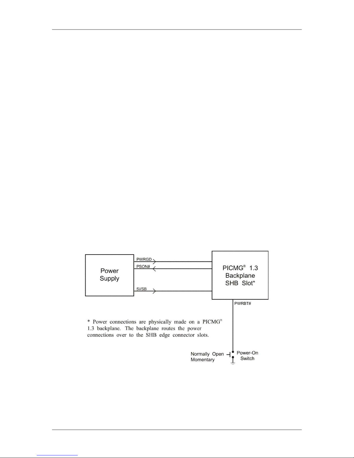
JXT6966 / JXTS6966 Technical Reference Power Connection
Chapter 3 JXT6966 / JXTS6966 System Power Connections
Introduction
The combination of new power supply technologies and the system capabilities defined in the SHB
Express® (PICMG® 1.3) specification requires a different approach to connecting system power to a
PICMG 1.3 backplane and/or SHB hardware.
To improve system MTTR (Mean Time To Repair), the PICMG 1.3 specification defines enough power
connections to the SHB’s edge connectors to eliminate the need to connect auxiliary power to the SHB. All
power connections in a PICMG 1.3 system can be made to the PICMG 1.3 backplane. This is true for
SHBs that use high-performance processors. The connectors on a backplane must have an adequate
number of contacts that are sufficiently rated to safely deliver the necessary power to drive these highperformance SHBs. Chassis Plans’ PICMG 1.3 backplanes define ATX/EPS and +12V connectors that are
compatible with ATX/EPS power supply cable harnesses and provide multiple pins capable of delivering
the current necessary to power high-performance processors.
The PICMG® 1.3 specification supports soft power control signals via the Advanced Configuration and
Power Interface (ACPI). Chassis Plans SHBs support these signals, which are controlled by the ACPI and
are used to implement various sleep modes. Refer to the General ACPI Configuration section of the
Advanced Setup chapter in this manual for information on ACPI BIOS settings.
When soft control signals are implemented, the type of ATX or EPS power supply used in the system and
the operating system software will dictate how system power should be connected to the SHB. It is critical
that the correct method be used.
Power Supply and SHB Interaction
The following diagram illustrates the interaction between the power supply and the processor. The signals
shown are PWRGD (Power Good), PSON# (Power Supply On), 5VSB (5 Volt Standby) and PWRBT#
(Power Button). The +/- 12V, +/-5V, +3.3V and Ground signals are not shown.
PWRGD, PSON# and 5VSB are usually connected directly from an ATX or EPS power supply to the
backplane. The PWRBT# is a normally open momentary switch that can be wired directly to a power
button on the chassis.
3-1 CHASSIS PLANS
Power Supply and SHB Interaction
Page 40

Power Connection JXT6966 / JXTS6966 Technical Reference
Signal
Description
Source
+12
DC voltage for those systems that require it
Power Supply
+5V
DC voltage for those systems that require it
Power Supply
+3.3V
DC voltage for those systems that require it
Power Supply
+5VSB
5 Volt Standby. This DC voltage is always on when an
ATX or EPS type power supply has AC voltage
connected. 5VSB is used to keep the necessary
circuitry functioning for software power control and
wake up.
Power Supply
PWRGD
Power Good. This signal indicates that the power
supply’s voltages are stable and within tolerance.
Power Supply
PSON#
Power Supply On. This signal is used to turn on an
ATX or EPS type power supply.
SHB/Backplane
PWRBT#
Power Button. A momentary normally open switch is
connected to this signal. When pressed and released,
this signals the SHB to turn on a power supply that is
in an off state.
If the system is on, holding this button for four
seconds will cause the SHB’s chipset to shut down
the power supply. The operating system is not
involved and therefore this is not considered a clean
shutdown. Data can be lost if this situation occurs.
Power Button
CAUTION: In some ATX/EPS systems, the power may appear to be off while the 5VSB signal is still
present and supplying power to the SHB, option cards and other system components. The +5VAUX LED
on a Chassis Plans PICMG 1.3 backplane monitors the 5VSB power signal; “green” indicates that the
5VSB signal is present. Chassis Plans backplane LEDs monitor all DC power signals, and all of the LEDs
should be off before adding or removing components. Removing boards under power may result in system
damage.
Electrical Connection Configurations
There are a number of different connector types, such as EPS, ATX or terminal blocks, which can be
utilized in wiring power supply and control functions to a PICMG 1.3 backplane. However, there are only
two basic electrical connection configurations: ACPI Connection and Legacy Non-ACPI Connection.
ACPI Connection
The diagram on the previous page shows how to connect an ACPI compliant power supply to an ACPI
enabled PICMG 1.3 system. The following table shows the required connections that must be made for
soft power control to work.
CHASSIS PLANS 3-2
Page 41

JXT6966 / JXTS6966 Technical Reference Power Connection
Signal
Description
Source
+12
DC voltage for those systems that require it
Power Supply
+5V
DC voltage for those systems that require it
Power Supply
+3.3V
DC voltage for those systems that require it
Power Supply
+5VSB
Not Required
Power Supply
PWRGD
Not Required
Power Supply
PSON#
Power Supply On. This signal is used to turn on an
ATX or EPS type power supply. If an ATX or EPS
power supply is used in this legacy configuration, a
shunt must be installed on the backplane from
PSON# to signal Ground. This forces the power
supply DC outputs on whenever AC to the power
supply is active.
Backplane
PWRBT#
Not Used
Legacy Non-ACPI Connection
For system integrators that either do not have or do not require an ACPI compliant power supply as
described in the section above, an alternative electrical configuration is described in the table on the
following page.
In addition to these connections, there is usually a switch controlling AC power input to the power supply.
When using the legacy electrical configuration, the SHB BIOS Power Supply Shutoff setting should be set
to Manual shutdown. Refer to the General ACPI Configuration section of the Advanced Setup chapter in
this manual for details.
3-3 CHASSIS PLANS
Page 42

Power Connection JXT6966 / JXTS6966 Technical Reference
This page intentionally left blank
CHASSIS PLANS 3-4
Page 43

JXT6966 / JXTS6966 Technical Reference PCI Express Backplane Usage
Chapter 4 PCI Express Backplane Usage
Introduction
PCI Express® is a scalable, full-duplex serial interface which consists of multiple communication lanes
grouped into links. PCI Express scalability is achieved by grouping these links into multiple
configurations. A x1 (“by 1”) PCI Express link is made up of one full-duplex link that consists of two
dedicated lanes for receiving data and two dedicated lanes for transmitting data. A x4 configuration is
made up of four PCI Express links. The most commonly used PCIe link sizes are x1, x4, x8 and x16.
PCI Express devices with different PCI Express link configurations establish communication with each
other using a process called auto-negotiation or link training. For example, a PCI Express device or option
card that has a x16 PCI Express interface and is placed into a x16 mechanical/x8 electrical slot on a
backplane establishes communication with a PICMG® 1.3 SHB using auto-negotiation. The option card’s
PCI Express interface will “train down” to establish communication with the SHB via the x8 PCI Express
link between the SHB and the backplane option card slot.
SHB Edge Connectors
The PICMG 1.3 specification enables SHB vendors to provide multiple PCI Express configuration options
for edge connectors A and B of a particular SHB. These edge connectors carry the PCI Express links and
reference clocks down to the SHB slot on the PICMG 1.3 backplane. The potential PCI Express link
configurations of an SHB fall into three main classifications: server-class, graphics-class and conbo-class.
The specific class and PCI Express link configuration of an SHB is determined by the chipset components
used on the SHB.
In a server-class configuration, the main goal of the SHB is to route as many high-bandwidth PCI Express
links as possible down to the backplane. Typically, these links are a combination of x4 and x8 PCI Express
links.
A graphics-class configuration should provide a x16 PCI Express link down to the backplane in order to
support high-end PCI Express graphics and video cards. Graphics-class SHB configurations also provide as
many lower bandwidth (x1 or x4) links as possible.
A combo-class configuration is provided by SHBs like the JXT6966 or JXTS6966. These system host
board types have PCI Express hardware and software implementations that are capable of combining links
to support either server or graphics-class PICMG 1.3 backplane configurations.
The PCI Express links on the JXT6966 / JXTS6966 connect directly to the processors. These links can
operate as either PCI Express 2.0 or PCI Express 1.1 links based on the end-point devices on the backplane
that connect to the SHB. In addition to automatically configuring themselves for either PCIe 2.0 or PCIe
1.1 operations, the links also configure themselves for either graphics or server-class operations. In other
words, the multiple x4 links from the processors; links A0, A1, A2 and A3, can be combined into a single
x16 PCIe electrical link or multiple x8 links on a backplane. The CPU’s x4 links can train down to x1
links, but cannot bifurcate into multiple x1 links. The PCIe link (B0) from the board’s PCH has a x4
default configuration and can be made to bifurcate into four, x1 PCIe links with a factory modification to
the JXT board. Contact Chassis Plans if you require this B0 link configuration change. An optional
PEX10 module connected to a dual-processor JXT6966 provides more backplane links than are currently
supported in the PICMG 1.3 specification. This JXT6966 capability provides additional PCI Express
bandwidth and option card support in the system design.
In addition to the standard PICMG 1.3 edge connector PCIe interfaces and the PEX10 expansion links, the
JXT boards also have an additional x1 link available for use on a backplane. This extra x1 link is routed to
the SHB’s controlled impedance connector for use with the Chassis Plans IOB33 plug-in option card. The
IOB33 routes this x1 PCI Express link down to a physical x4 PCIe edge connector on the board. A x4
connector is used so that the IOB33 can be used on other Chassis Plans SHBs that may support a x4 PCIe
expansion link rather than a x1. The electrical width of this expansion link is determined by the board’s
4-1 CHASSIS PLANS
Page 44

PCI Express Backplane Usage JXT6966 / JXTS6966 Technical Reference
chipset. The IOB33 edge connector mates with a backplane’s PCIe Expansion slot. This extra link is
useful in supporting an additional system card slot. Refer to the IOB Expansion Board - Appendix D for
more information the IOB33 and the PCI Express Reference chapter for more information on the PCI
Express signal routings to the SHB edge connectors.
The figures below show some typical SHB and backplane combinations that would result in all of the PCI
Express slots successfully establishing communication with the SHB host device. The first figure shows a
server-class SHB; the second shows a graphics-class SHB.
PCI Express link configuration straps for each PCI Express option card slot on a PICMG 1.3 backplane are
required as part of the PICMG 1.3 SHB Express® specification. These configuration straps alert the SHB
as to the specific link configuration expected on each PCI Express option card slot. PCI Express
communication between the SHB and option card slots is successful only when there are enough available
PCI Express links established between the PICMG 1.3 SHB and each PCI Express slot or device on the
backplane.
For more information, refer to the PCI Industrial Manufacturers Group’s SHB Express® System Host
Board PCI Express Specification, PICMG® 1.3.
CHASSIS PLANS 4-2
Page 45

JXT6966 / JXTS6966 Technical Reference PCI Express Backplane Usage
PICMG 1.3 Backplane
Compatible with JXT6966 (i.e. all
backplane slots are functional)
Why not or clarification
2U Butterfly Backplanes
BPG6741
Yes
BPX6736
Yes
Multi-Segment Backplanes
BP6FS6605
No
SHB segment spacing
BP4FS6890
Yes, for both SC and GC config.
BP2S6929
Yes
Combo Backplanes
BPC7041
Yes for the JXT6966 with a PEX10 No
for the JXTS6966 single CPU
CPU2 provides the links for BP
slots PCIe 1 through PCIe4
BPC7009
Yes
Server-Class Backplanes
BPX6806
Yes, need IOB33 for PCIe1 slot
JXT6966 provides x1 via IOB33
BPX6620
Yes, need IOB33 for PCIe1 slot
JXT6966 provides x1 via IOB33
BPX6610
Yes
BPX6571
Yes BPX3/14
Yes, need IOB33 for PCIe2 slot
JXT6966 provides x1 via IOB33
BPX3/8
Yes
BPX6719
Yes, need IOB33 for PCIe1 slot
JXT6966 provides x1 via IOB33
BPX3/2
Yes BPX5
Yes, need IOB33 for PCIe1 slot
JXT6966 provides x1 via IOB33
Graphics-Class Backplanes
BPG6615
Yes
BPG6600
No
32b/33MHz slots C1, C2, C3 & C4
are inoperative when using a
JXT6966 SHB
BPG6544
No
32b/33MHz slots C1, C2, & ISA
slots D1 & D2 are inoperative when
using a JXT6966 SHB
BPG6714
Yes, need IOB33 for PCIe1 slot
JXT6966 provides x1 via IOB33
BPG2/2
Yes
BPG4
Yes, need IOB33 for PCIe1 slot
JXT6966 provides x1 via IOB33
Off-Board Video Card Usage
If the system design requires an off-board video card, then the card must be placed in a backplane slot
driven with PCI Express links from the JXT6966’s first processor. This is an Aptio® 4.x BIOS limitation
that may be corrected in future software revisions. Listed below are the acceptable BPC7009 and BPC7041
backplane slots for use with an off-board video card:
BPC7009 - Card slot PCIe1, PCIe2 or PCIe3
BPC7041 - Card slot PCIe6, PCIe7, PCIe8, PCIe9 or PCIe10
JXT6966 & JXTS6966 and Compatible Chassis Plans Backplanes
The JXT6966 and JXTS6966 are standard PICMG 1.3 SHBs that will function with a wide variety of
industry standard PICMG 1.3 backplanes. However, some non-Chassis Plans backplane may not utilize to
full capabilities of the Chassis Plans JXT6966 and JXTS6966 boards. The table below illustrates the JXT
compatibility with the current listing of Chassis Plans PICMG 1.3 backplanes. A “Yes” in the compatible
column below means that all slots on the backplane will function with a JXT6966 board. The clarification
column explains any limitations of using either a JXT6966 dual-processor or a JXTS-6966 single processor
SHB with a particular backplane. Chassis Plans continuously adds backplanes to our product line, so
contact us or visit our website for the latest backplane availability listings
4-3 CHASSIS PLANS
Page 46

PCI Express Backplane Usage JXT6966 / JXTS6966 Technical Reference
CHASSIS PLANS 4-4
Page 47

JXT6966 / JXTS6966 Technical Reference PCI Express Backplane Usage
This page intentionally left blank
4-5 CHASSIS PLANS
Page 48

Page 49

JKXT6966 / JXTS6966 Technical Reference I/O Expansion Boards
IOB Module
T4L
(S6483)
TML
(S6490)
TQ9
(S6731)
MCG-
Series
(S6680,
S6690,
S6675,
S6695)
NLI /
NLT
(S6313,
S6396)
SLT / SLI
(S6515,
S6521)
MCX-
Series
(S6633,
S6685,
S6638,
S6700)
JXT / JXTS
(S6966)
IOB33JX
(S7015-004)
X
IOB33MC
(S7015-002)
X X X
IOB33
(S7015-000)
X X X X
Chapter 5 I/O Expansion Boards – IOB33 & PEX10
IOB33 Overview
The IOB33 is optional I/O expansion board designed for use with the JXT6966 and JXTS6966 SHBs.
Additional board versions are available for use with other Chassis Plans SHBs. The IOB33 provides legacy
I/O support and features a x4 PCIe edge connector along the bottom edge of the card. This x4 card edge
connector routes a x1PCI Gen 1.1 electrical link from the boards Intel® 3420 PCH down to the expansion
slot on a PICMG 1.3 backplane. The electrical width of this expansion link is determined by the board’s
chipset. For example, an IOB33 used with a Chassis Plans MCX/MCG will route a x4 PCIe link from the
south bridge of these SHBs down to a backplane. This extra link is useful in supporting an additional
system card slot.
The optional IOB33 also expands the I/O capabilities of the system. The IOB33 has the following
interfaces available for use by the system designer:
Two - RS232 communication ports
One - Floppy drive interface
One - Parallel printer interface
One – PS/2 Mini-DIN connector for PS/2 keyboard and mouse connections
Also includes separate, on-board PS/2 keyboard and mouse headers for systems
that require separate PS/2 connections
There are three versions of the Chassis Plans IOB33 I/O expansion board. This optional board is designed
for the JXT6966 and JXTS6966 SHBs, but the additional versions may be used on other Chassis Plans
SHBs. The chart below identifies the IOB33 version that is compatible with specific Chassis Plans SHBs.
IOB33 Models
Model # Model Name Description
S7015-004 IOB33JX Includes the I/O Plate for use with the JXT6966 or
JXTS6966 System Host Boards
S7015-002 IOB33MC Includes the I/O Plate for use with MCX, MCG and
TQ9 system host boards
S7015-000 IOB330 Includes the I/O Plate for use with TML, SLT, SLI,
NLT, NLI and T4L system host boards
5-1 CHASSIS PLANS
Page 50
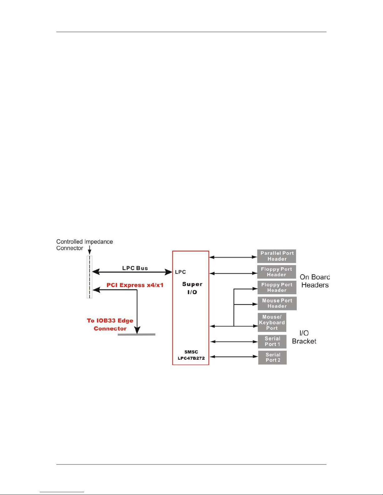
I/O Expansion Boards JXT6966 / JXTS6966 Technical Reference
IOB33 Features
IOB33 (7015-004, 7015-002, 7015-001)
I/O plate versions for a variety of Chassis Plans system host boards
Two serial ports and PS/2 mouse/keyboard mini DIN on the I/O bracket
PS/2 mouse, keyboard, parallel port and floppy drive connectors
PCI Express expansion capability for use with PCI Express backplanes
Compatible with PCI Industrial Computer Manufacturers Group (PICMG®) PCI Express
Specification
IOB33 Temperature/Environment
Operating Temperature: 0º C. to 60º C.
Storage Temperature: -20º C. to 70º C.
Humidity: 5% to 90% non-condensing
IOB33 (S7015-xxx) Block Diagram
CHASSIS PLANS 5-2
Page 51
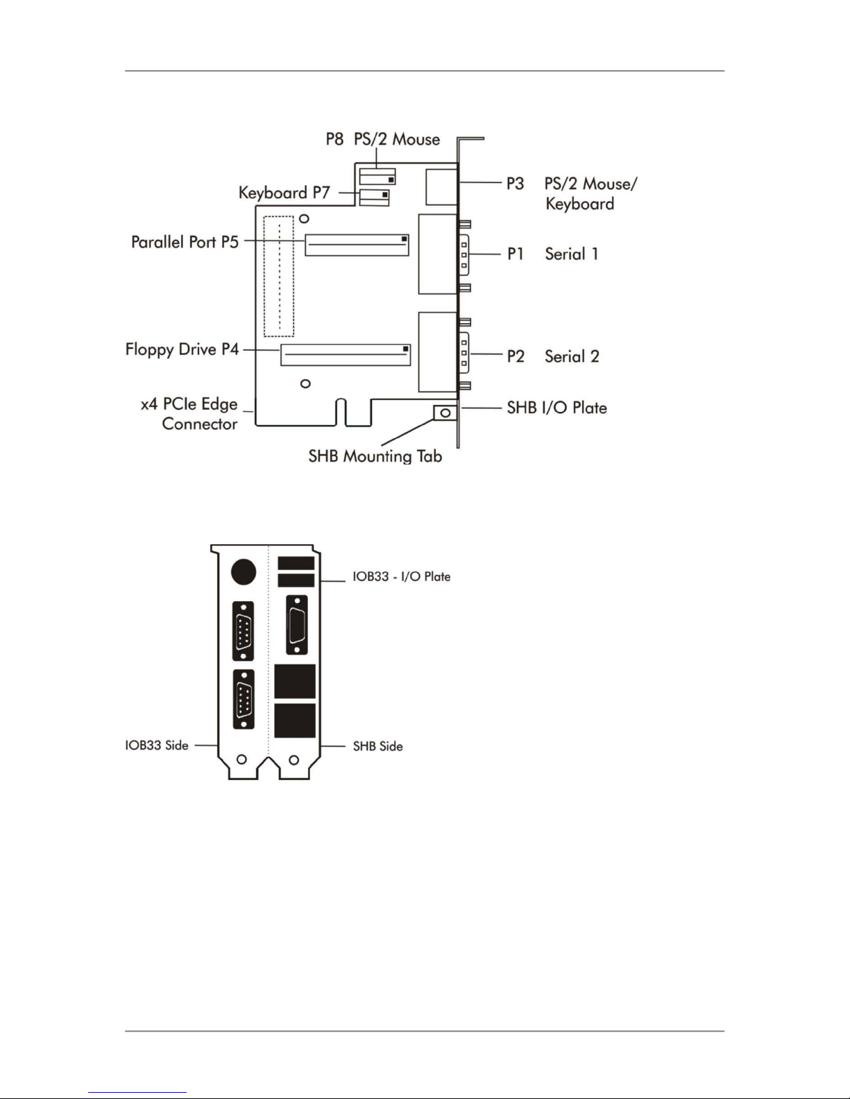
JKXT6966 / JXTS6966 Technical Reference I/O Expansion Boards
IOB33 (S7015-xxx) Layout Diagram
IOB33 (S7015-xxx) I/O Plate Diagram
5-3 CHASSIS PLANS
Page 52

I/O Expansion Boards JXT6966 / JXTS6966 Technical Reference
P1 - Serial Port Connector
9 position “D” right angle, Spectrum #56-402-001
Pin
Signal
Pin
Signal
1
Carrier Detect
6
Data Set Ready-I
2
Receive Data-I
7
Request to Send-O
3
Transmit Data-O
8
Clear to Send-
4
Data Terminal Ready-O
9
Ring Indicator-I
5
Signal Gnd
P2 - Serial Port Connector
9 position “D” right angle, Spectrum #56-402-001
Pin
Signal
Pin
Signal
1
Carrier Detect
6
Data Set Ready-I
2
Receive Data-I
7
Request to Send-O
3
Transmit Data-O
8
Clear to Send-
4
Data Terminal Ready-O
9
Ring Indicator-I
5
Signal Gnd
P3 - PS/2 Mouse and Keyboard Connector
6 pin mini DIN, Kycon #KMDG-6S-B4T
Pin
Signal
1
Ms Data
2
Kbd Data
3
Gnd
4
Power (+5V fused) with self-resetting fuse
5
Ms Clock
6
Kbd Clock
P4 - Floppy Drive Connector
34 pin dual row header, Amp #103308-7
Pin
Signal
Pin
Signal
1
Gnd 2 N-RPM
3
Gnd 4 NC 5 Gnd 6 D-Rate0
7
Gnd 8 P-Index
9
Gnd
10
N-Motoron 1
11
Gnd
12
N-Drive Sel2
13
Gnd
14
N-Drive Sel1
15
Gnd
16
N-Motoron 2
17
Gnd
18
N-Dir
19
Gnd
20
N-Stop Step
21
Gnd
22
N-Write Data
23
Gnd
24
N-Write Gate
25
Gnd
26
P-Track 0
27
Gnd
28
P-Write Protect
29
Gnd
30
N-Read Data
31
Gnd
32
N-Side Select
33
Gnd
34
Disk Change
IOB33 Connectors
NOTE: Pin 1 on the connectors is indicated by the square pad on the PCB.
CHASSIS PLANS 5-4
Page 53

JKXT6966 / JXTS6966 Technical Reference I/O Expansion Boards
P5 - Parallel Port Connector
26 pin dual row header, Amp #103308-6
Pin
Signal
Pin
Signal
1
Strobe
2
Auto Feed XT
3
Data Bit 0
4
Error
5
Data Bit 1
6
Init 7 Data Bit 2
8
Slct In
9
Data Bit 3
10
Gnd
11
Data Bit 4
12
Gnd
13
Data Bit 5
14
Gnd
15
Data Bit 6
16
Gnd
17
Data Bit 7
18
Gnd
19
ACK
20
Gnd
21
Busy
22
Gnd
23
Paper End
24
Gnd
25
Slct
26
NC
P7 - Keyboard Header
5 pin single row header, Amp #640456-5
Pin
Signal
1
Kbd Clock
2
Kbd Data
3
Key
4
Kbd Gnd
5
Kbd Power (+5V fused) with self resetting fuse
P8 - PS/2 Mouse Header
6 pin single row header, Amp #640456-6
Pin
Signal
1
Ms Data
2
Reserved
3
Gnd 4 Power (+5V fused) with self-resetting fuse
5
Ms Clock
6
Reserved
IOB33 Connectors (continued)
5-5 CHASSIS PLANS
Page 54

I/O Expansion Boards JXT6966 / JXTS6966 Technical Reference
P6 - Impedance Connector
76 pin controlled impedance connector,
Samtec #MIS-038-01-FD-K
Pin
Signal
Pin
Signal
1
+12 2 +5V_STANDBY
3
NC 4 +5V_STANDBY
5
NC 6 +5V_DUAL
7
NC 8 +5V_DUAL
9
NC
10
NC
11
NC
12
NC
13
ICH_SMI#
14
ICH_RCIN#
15
ICH_SIOPME#
16
ICH_A20GATE
17
Gnd
18
Gnd
19
L_FRAME#
20
L_AD3
21
L_DRQ1#
22
L_AD2
23
L_DRQ0#
24
L_AD1
25
SERIRQ
26
L_AD0
27
Gnd
28
Gnd
29
PCLK14SIO
30
PCLK33LPC
31
Gnd
32
Gnd
33
SMBDATA_RESUME
34
IPMB_DAT
35
SBMCLK_RESUME
36
IPMB_CLK
37
SALRT#_RESUME
38
IPMB_ALRT#
39
Gnd
40
Gnd
41
EXP_CLK100
42
EXP_RESET#
43
EXP_CLK100#
44
ICH_WAKE#
45
Gnd
46
Gnd
47
C_PE_TXP4
48
C_PE_RXP4
49
C_PE_TXN4
50
C_PE_RXN4
51
Gnd
52
Gnd
53
C_PE_TXP3
54
C_PE_RXP3
55
C_PE_TXN3
56
C_PE_RXN3
57
Gnd
58
Gnd
59
C_PE_TXP2
60
C_PE_RXP2
61
C_PE_TXN2
62
C_PE_RXN2
63
Gnd
64
Gnd
65
C_PE_TXP1
66
C_PE_RXP1
67
C_PE_TXN1
68
C_PE_RXN1
69
Gnd
70
Gnd
71
+3.3V
72
+5V
73
+3.3V
74
+5V
75
+3.3V
76
+5v
IOB33 CONNECTORS (CONTINUED)
CHASSIS PLANS 5-6
Page 55

JKXT6966 / JXTS6966 Technical Reference I/O Expansion Boards
PEX10 Overview
The PEX10 is an optional PCIe link expansion board that takes advantage of the additional PCI Express 2.0
interfaces supported on the Intel® Xeon® EC5500/LC5500-series (i.e. Jasper Forest) processors.
Direct PCI Express 2.0 interfaces from the Jasper Forest processors are a compelling feature of Chassis
Plans’ JXT6966 and JXTS6966 system host boards. The JXT6966 is a dual-processor SHB with more
available PCIe links than the 20 PCIe links currently defined in the PICMG® 1.3 SHB Express® industry
specification. Many system designs could utilize the additional 16 PCIe links offered by second processor
on a Chassis Plans JXT6966 SHB to increase a systems data bandwidth and information throughput. The
PEX10 is an optional PCI Express expansion board that makes these addition 16 links available to the
system designer.
The PEX10 is a passive board that mounts to the back of a Chassis Plans JXT6966. This PEX10 passive
interface card routes the four additional PCIe 2.0 x4 electrical links from second processor on a JXT6966
down to a mechanical x16 PCIe link expansion slot on the backplane. The Chassis Plans BPC7009 and
BPC7041 backplanes support this additional PCI Express 2.0 link expansion slot. The multiple x4 PCIe
links are connected directly to option card slots on the passive BPC7041 backplane. PCIe Gen 2 link redrivers are used on the BPC7041backplane to ensure signal integrity between the SHB and the option card.
The x4 links on a BPC7009 backplane are routed to PCIe switching devices to ensure signal integrity and
to combine the x4 links into x8 electrical links for use on selected option card slots and other backplane
devices.
NOTE:
Currently, the PEX10 is compatible with only the Chassis Plans JXT6966 SHB and the Chassis
Plans BPC7009 and BPC7041 backplanes. Chassis Plans is constantly expanding its PCI Express
backplane product offerings. See the Chassis Plans website or contact us for additional backplane
availability.
5-7 CHASSIS PLANS
Page 56

I/O Expansion Boards JXT6966 / JXTS6966 Technical Reference
This page intentionally left blank
CHASSIS PLANS 5-8
Page 57

JXT6966 / JXTS6966 Technical Reference BIOS Messages
# of Beeps
Description
1
Memory not Installed
1
Memory was installed twice (InstallPeiMemory routine in PEI Core called twice)
2
Recovery started
3
DXEIPL was not found
3
DXE Core Firmware Volume was not found
7
Reset PPI is not available
4
Recovery failed
4
S3 Resume failed
Appendix A BIOS Messages
Introduction
A status code is a data value used to indicate progress during the boot phase. These codes are outputed to
I/O port 80h on the SHB. Aptio 4.x core outputs checkpoints throughout the boot process to indicate the
task the system is currently executing. Status codes are very useful in aiding software developers or
technicians in debugging problems that occur during the pre-boot process.
Aptio Boot Flow
While performing the functions of the traditional BIOS, Aptio 4.x core follows the firmware model
described by the Intel Platform Innovation Framework for EFI (“the Framework”). The Framework refers
the following “boot phases”, which may apply to various status code descriptions:
Security (SEC) – initial low-level initialization
Pre-EFI Initialization (PEI) – memory initialization1
Driver Execution Environment (DXE) – main hardware initialization2
Boot Device Selection (BDS) – system setup, pre-OS user interface & selecting a bootable
device (CD/DVD, HDD, USB, Network, Shell, …)
1
Analogous to “bootblock” functionality of legacy BIOS
2
Analogous to “POST” functionality in legacy BIOS
BIOS Beep Codes
The Pre-EFI Initialization (PEI) and Driver Execution Environment (DXE) phases of the Aptio BIOS use
audible beeps to indicate error codes. The number of beeps indicates specific error conditions.
PEI Beep Codes
A-1 CHASSIS PLANS
Page 58

BIOS Messages JXT6966 / JXTS6966 Technical Reference
# of Beeps
Description
4
Some of the Architectural Protocols are not available
5
No Console Output Devices are found
5
No Console Input Devices are found
1
Invalid password
6
Flash update is failed
7
Reset protocol is not available
8
Platform PCI resource requirements cannot be met
DXE Beep Codes
CHASSIS PLANS A-2
Page 59
JXT6966 / JXTS6966 Technical Reference BIOS Messages
Upper Nibble (UN)
Lower Nibble (LN)
Hex.
Value
LED7
LED6
LED5
LED4
Hex.
Value
LED3
LED2
LED1
LED0
0
Off
Off
Off
Off
0
Off
Off
Off
Off 1 Off
Off
Off
On
1
Off
Off
Off
On
2
Off
Off
On
Off
2
Off
Off
On
Off
3
Off
Off
On
On 3
Off
Off
On
On 4 Off
On
Off
Off 4
Off
On
Off
Off
5
Off
On
Off
On 5
Off
On
Off
On 6 Off
On
On
Off 6
Off
On
On
Off 7 Off
On
On
On 7
Off
On
On
On
8
On
Off
Off
Off 8
On
Off
Off
Off 9 On
Off
Off
On 9
On
Off
Off
On A On
Off
On
Off A
On
Off
On
Off
B
On
Off
On
On B
On
Off
On
On C On
On
Off
Off C
On
On
Off
Off
D
On
On
Off
On D
On
On
Off
On E On
On
On
Off E
On
On
On
Off F On
On
On
On F
On
On
On
On
Lower Nibble
7 6 5 4 3 2 1 0
Upper Nibble
JXT6966 & JXTS6966 POST Code LEDs
BIOS Status Codes
As the POST (Power On Self Test) routines are performed during boot-up, test codes are displayed on Port
80 POST code LEDs 0, 1, 2, 3, 4, 5, 6 and 7. These LED are located on the top of the SHB, just above the
board’s battery socket. The POST Code LEDs and are numbered from right (position 1 = LED0) to left
(position 8 – LED7).
The POST code checkpoints are the largest set of checkpoints during the BIOS pre-boot process. The
following chart is a key to interpreting the POST codes displayed on LEDs 0 through 7 on the JXT6966
and JXTS6966 SHBs. Refer to the board layout in the Specifications chapter for the exact location of the
POST code LEDs.
The HEX to LED chart in the POST Code LEDs section will serve as a guide to interpreting specific BIOS
status codes.
BIOS Status POST Code LEDs
As the POST (Power On Self Test) routines are performed during boot-up, test codes are displayed on Port
80 POST code LEDs 0, 1, 2, 3, 4, 5, 6 and 7. These LED are located on the top of the SHB, just above the
board’s battery socket. The POST Code LEDs and are numbered from right (position 1 = LED0) to left
(position 8 – LED7).
The POST code checkpoints are the largest set of checkpoints during the BIOS pre-boot process. The
following chart is a key to interpreting the POST codes displayed on LEDs 0 through 7 on the JXT6966
and JXTS6966 SHBs. Refer to the board layout in the Specifications chapter for the exact location of the
POST code LEDs.
A-3 CHASSIS PLANS
Page 60

BIOS Messages JXT6966 / JXTS6966 Technical Reference
Status Code Range
Description
0x01 – 0x0F
SEC Status Codes & Errors
0x10 – 0x2F
PEI execution up to and including memory detection
0x30 – 0x4F
PEI execution after memory detection
0x50 – 0x5F
PEI errors
0x60 – 0xCF
DXE execution up to BDS
0xD0 – 0xDF
DXE errors
0xE0 – 0xE8
S3 Resume (PEI)
0xE9 – 0xEF
S3 Resume errors (PEI)
0xF0 – 0xF8
Recovery (PEI)
0xF9 – 0xFF
Recovery errors (PEI)
Status Code
Description
0x0
Not used
Progress Codes
0x1
Power on. Reset type detection (soft/hard).
0x2
AP initialization before microcode loading
0x3
North Bridge initialization before microcode loading
0x4
South Bridge initialization before microcode loading
0x5
OEM initialization before microcode loading
0x6
Microcode loading
0x7
AP initialization after microcode loading
0x8
North Bridge initialization after microcode loading
0x9
South Bridge initialization after microcode loading
0xA
OEM initialization after microcode loading
0xB
Cache initialization
SEC Error Codes
0xC – 0xD
Reserved for future AMI SEC error codes
0xE
Microcode not found
0xF
Microcode not loaded
Status Code Ranges
SEC Status Codes
SEC Beep Codes
There are no SEC Beep codes associated with this phase of the Aptio BIOS boot process.
CHASSIS PLANS A-4
Page 61

JXT6966 / JXTS6966 Technical Reference BIOS Messages
Status Code
Description
Progress Codes
0x10
PEI Core is started
0x11
Pre-memory CPU initialization is started
0x12
Pre-memory CPU initialization (CPU module specific)
0x13
Pre-memory CPU initialization (CPU module specific)
0x14
Pre-memory CPU initialization (CPU module specific)
0x15
Pre-memory North Bridge initialization is started
0x16
Pre-Memory North Bridge initialization (North Bridge module specific)
0x17
Pre-Memory North Bridge initialization (North Bridge module specific)
0x18
Pre-Memory North Bridge initialization (North Bridge module specific)
0x19
Pre-memory South Bridge initialization is started
0x1A
Pre-memory South Bridge initialization (South Bridge module specific)
0x1B
Pre-memory South Bridge initialization (South Bridge module specific)
0x1C
Pre-memory South Bridge initialization (South Bridge module specific)
0x1D – 0x2A
OEM pre-memory initialization codes
0x2B
Memory initialization. Serial Presence Detect (SPD) data reading
0x2C
Memory initialization. Memory presence detection
0x2D
Memory initialization. Programming memory timing information
0x2E
Memory initialization. Configuring memory
0x2F
Memory initialization (other).
0x30
Reserved for ASL (see ASL Status Codes section below)
0x31
Memory Installed
0x32
CPU post-memory initialization is started
0x33
CPU post-memory initialization. Cache initialization
0x34
CPU post-memory initialization. Application Processor(s) (AP) initialization
0x35
CPU post-memory initialization. Boot Strap Processor (BSP) selection
0x36
CPU post-memory initialization. System Management Mode (SMM) initialization
0x37
Post-Memory North Bridge initialization is started
0x38
Post-Memory North Bridge initialization (North Bridge module specific)
0x39
Post-Memory North Bridge initialization (North Bridge module specific)
0x3A
Post-Memory North Bridge initialization (North Bridge module specific)
0x3B
Post-Memory South Bridge initialization is started
0x3C
Post-Memory South Bridge initialization (South Bridge module specific)
0x3D
Post-Memory South Bridge initialization (South Bridge module specific)
0x3E
Post-Memory South Bridge initialization (South Bridge module specific)
0x3F-0x4E
OEM post memory initialization codes
0x4F
DXE IPL is started
PEI Status Codes
A-5 CHASSIS PLANS
Page 62

BIOS Messages JXT6966 / JXTS6966 Technical Reference
PEI Error Codes
0x50
Memory initialization error. Invalid memory type or incompatible memory speed
0x51
Memory initialization error. SPD reading has failed
0x52
Memory initialization error. Invalid memory size or memory modules do not match.
0x53
Memory initialization error. No usable memory detected
0x54
Unspecified memory initialization error.
0x55
Memory not installed
0x56
Invalid CPU type or Speed
0x57
CPU mismatch
0x58
CPU self test failed or possible CPU cache error
0x59
CPU micro-code is not found or micro-code update is failed
0x5A
Internal CPU error
0x5B
reset PPI is not available
0x5C-0x5F
Reserved for future AMI error codes
S3 Resume Progress Codes
0xE0
S3 Resume is stared (S3 Resume PPI is called by the DXE IPL)
0xE1
S3 Boot Script execution
0xE2
Video repost
0xE3
OS S3 wake vector call
0xE4-0xE7
Reserved for future AMI progress codes
0xE0
S3 Resume is stared (S3 Resume PPI is called by the DXE IPL)
S3 Resume Error Codes
0xE8
S3 Resume Failed in PEI
0xE9
S3 Resume PPI not Found
0xEA
S3 Resume Boot Script Error
0xEB
S3 OS Wake Error
0xEC-0xEF
Reserved for future AMI error codes
Recovery Progress Codes
0xF0
Recovery condition triggered by firmware (Auto recovery)
0xF1
Recovery condition triggered by user (Forced recovery)
0xF2
Recovery process started
0xF3
Recovery firmware image is found
0xF4
Recovery firmware image is loaded
0xF5-0xF7
Reserved for future AMI progress codes
Recovery Error Codes
0xF8
Recovery PPI is not available
0xF9
Recovery capsule is not found
0xFA
Invalid recovery capsule
0xFB – 0xFF
Reserved for future AMI error codes
CHASSIS PLANS A-6
Page 63

JXT6966 / JXTS6966 Technical Reference BIOS Messages
# of Beeps
Description
1
Memory not Installed
1
Memory was installed twice (InstallPeiMemory routine in PEI Core called twice)
2
Recovery started
3
DXEIPL was not found
3
DXE Core Firmware Volume was not found
7
Reset PPI is not available
4
Recovery failed
4
S3 Resume failed
Status Code
Description
0x60
DXE Core is started
0x61
NVRAM initialization
0x62
Installation of the South Bridge Runtime Services
0x63
CPU DXE initialization is started
0x64
CPU DXE initialization (CPU module specific)
0x65
CPU DXE initialization (CPU module specific)
0x66
CPU DXE initialization (CPU module specific)
0x67
CPU DXE initialization (CPU module specific)
0x68
PCI host bridge initialization
0x69
North Bridge DXE initialization is started
0x6A
North Bridge DXE SMM initialization is started
0x6B
North Bridge DXE initialization (North Bridge module specific)
0x6C
North Bridge DXE initialization (North Bridge module specific)
0x6D
North Bridge DXE initialization (North Bridge module specific)
0x6E
North Bridge DXE initialization (North Bridge module specific)
0x6F
North Bridge DXE initialization (North Bridge module specific)
0x70
South Bridge DXE initialization is started
0x71
South Bridge DXE SMM initialization is started
0x72
South Bridge devices initialization
0x73
South Bridge DXE Initialization (South Bridge module specific)
0x74
South Bridge DXE Initialization (South Bridge module specific)
0x75
South Bridge DXE Initialization (South Bridge module specific)
0x76
South Bridge DXE Initialization (South Bridge module specific)
0x77
South Bridge DXE Initialization (South Bridge module specific)
0x78
ACPI module initialization
0x79
CSM initialization
PEI Beep Codes
DXE Status Codes
A-7 CHASSIS PLANS
Page 64

BIOS Messages JXT6966 / JXTS6966 Technical Reference
0x7A – 0x7F
Reserved for future AMI DXE codes
0x80 – 0x8F
OEM DXE initialization codes
0x90
Boot Device Selection (BDS) phase is started
0x91
Driver connecting is started
0x92
PCI Bus initialization is started
0x93
PCI Bus Hot Plug Controller Initialization
0x94
PCI Bus Enumeration
0x95
PCI Bus Request Resources
0x96
PCI Bus Assign Resources
0x97
Console Output devices connect
0x98
Console input devices connect
0x99
Super IO Initialization
0x9A
USB initialization is started
0x9B
USB Reset
0x9C
USB Detect
0x9D
USB Enable
0x9E – 0x9F
Reserved for future AMI codes
0xA0
IDE initialization is started
0xA1
IDE Reset
0xA2
IDE Detect
0xA3
IDE Enable
0xA4
SCSI initialization is started
0xA5
SCSI Reset
0xA6
SCSI Detect
0xA7
SCSI Enable
0xA8
Setup Verifying Password
0xA9
Start of Setup
0xAA
Reserved for ASL (see ASL Status Codes section below)
0xAB
Setup Input Wait
0xAC
Reserved for ASL (see ASL Status Codes section below)
0xAD
Ready To Boot event
0xAE
Legacy Boot event
0xAF
Exit Boot Services event
0xB0
Runtime Set Virtual Address MAP Begin
0xB1
Runtime Set Virtual Address MAP End
0xB2
Legacy Option ROM Initialization
0xB3
System Reset
0xB4
USB hot plug
0xB5
PCI bus hot plug
0xB6
Clean-up of NVRAM
0xB7
Configuration Reset (reset of NVRAM settings)
CHASSIS PLANS A-8
Page 65

JXT6966 / JXTS6966 Technical Reference BIOS Messages
0xB8 – 0xBF
Reserved for future AMI codes
0xC0 – 0xCF
OEM BDS initialization codes
DXE Error Codes
0xD0
CPU initialization error
0xD1
North Bridge initialization error
0xD2
South Bridge initialization error
0xD3
Some of the Architectural Protocols are not available
0xD4
PCI resource allocation error. Out of Resources
0xD5
No Space for Legacy Option ROM
0xD6
No Console Output Devices are found
0xD7
No Console Input Devices are found
0xD8
Invalid password
0xD9
Error loading Boot Option (LoadImage returned error)
0xDA
Boot Option is failed (StartImage returned error)
0xDB
Flash update is failed
0xDC
Reset protocol is not available
# of Beeps
Description
4
Some of the Architectural Protocols are not available
5
No Console Output Devices are found
5
No Console Input Devices are found
1
Invalid password
6
Flash update is failed
7
Reset protocol is not available
8
Platform PCI resource requirements cannot be met
DXE Beep Codes
A-9 CHASSIS PLANS
Page 66
BIOS Messages JXT6966 / JXTS6966 Technical Reference
Status Code
Description
0x01
System is entering S1 sleep state
0x02
System is entering S2 sleep state
0x03
System is entering S3 sleep state
0x04
System is entering S4 sleep state
0x05
System is entering S5 sleep state
0x10
System is waking up from the S1 sleep state
0x20
System is waking up from the S2 sleep state
0x30
System is waking up from the S3 sleep state
0x40
System is waking up from the S4 sleep state
0xAC
System has transitioned into ACPI mode. Interrupt controller is in PIC mode.
0xAA
System has transitioned into ACPI mode. Interrupt controller is in APIC mode.
Status Code
Description
0x5
OEM SEC initialization before microcode loading
0xA
OEM SEC initialization after microcode loading
0x1D – 0x2A
OEM pre-memory initialization codes
0x3F – 0x4E
OEM PEI post memory initialization codes
0x80 – 0x8F
OEM DXE initialization codes
0xC0 – 0xCF
OEM BDS initialization codes
ACPI/ASL Status Codes
OEM-Reserved Status Code Ranges
CHASSIS PLANS A-10
 Loading...