

Changhong Electric PT4216 Service Manual

1
PDP TELEVISION
SERVICE MANUAL
Chassis NO. PS08
Model No. PT4216
Please read this manual carefully before service.

2
CONTENTS
PartⅠ:PS08 Chassis Features and Circuit block diagram..………..............................3
PartⅡ:Introduction on main components functions of PT4216 ...……………………7
PartⅢ:Analysis on Signal Process Flow of PT4216 and key point test data ………..24
PartⅣ:Typical troubleshooting process flowchart of PT4216……..............................33
PartⅤ: Spare part list…………………………………………………………………...39
PartⅥ:Factory mode setup and attention…………………………………………40
Annex: 1、Circuit schematic diagram of PT4216……………………………………41
2、Final Assembly diagram of PT4216……....................................................60
3、Final Wire Connection diagram of PT4216………………………………61
3
PartⅠ:PS08 Chassis Features and Circuit block diagram
1、 PT4216/PT4218 Panel Datas:
PT4216/ PT4218 and PT5016 are all belong to PS08 chassis. The used panel parameter is below:
PDP Panel Resolution
852×3(RGB)×480
Colors 16,777,216
Dot Pitch
1.095mm(H)×1.110mm(V)
Brightness High brightness
Contrast High contrast
Lifespan of Panel 20000 Hours
Viewing Angle
U/D:160 / L/R:160
Valid display area
933mm(H)×533mm(V)
Remarks: Brightness and contrast may vary because of different panels being used. PT4216 mainly uses LG
PDP42V7 panel model or Panasonic MD42M7、MD42M8 panel model .注
2、Main Features:
z Radio Frequency input; support CATV
Capable to receive the full CATV programs.
z PIP function
z DVI digital RGB input
z VGA analog RGB input
z High definition YPbPr input
z AV input
Capable to receive NTSC/PAL/SECAM AV signal. Convenient to watch VCR,DVR,DVD programs. Make you into
perfect AV world.
z AV audio and video output
Capable to output one way video, left and right audio signal each one.
z Y/C component video input
S-video input, convenient to connect Y/C video input from DVD output.
z 236 programs preset
In TV condition, capable to save 236 programs. Ready for future rich programs.
z Multi format
Capable to receive NTSC/PAL/SECAM TV signal. Capable to receive D/K,I,B/G,M audio format TV signal.
z On/off on time
Set PDP TV on or off at preset time.
z Blue background mute noise
In TV, AV (S-Video), YCbCr, and YPbPr modes, screen displays gentle blue background if there is no signal input
and into mute condition.
z Auto Off if no signal input
In TV mode, the PDP TV will automatically power off within 15 minutes and enter into standby condition.
z Chinese/English menu
Ordinary and graphical user interface makes the menu operation more convenient and intuitionistic
z Power Energy Saving Mode (power management mode)
In PC mode, the PDD TV will automatically power off within 30 seconds and enter into the Power Energy Saving
Mode if there is no signal input. It will automatically exit from the Power Energy Saving Mode and work again
when it received a valid signal or press any button on the panel/remote control.
z Plug and Play
It is no need to equip any installation software when the product is used as computer terminal display equipment. It
4
is real plug and play.
z Little weight, small dimension, low power consumption
3、CBU Content
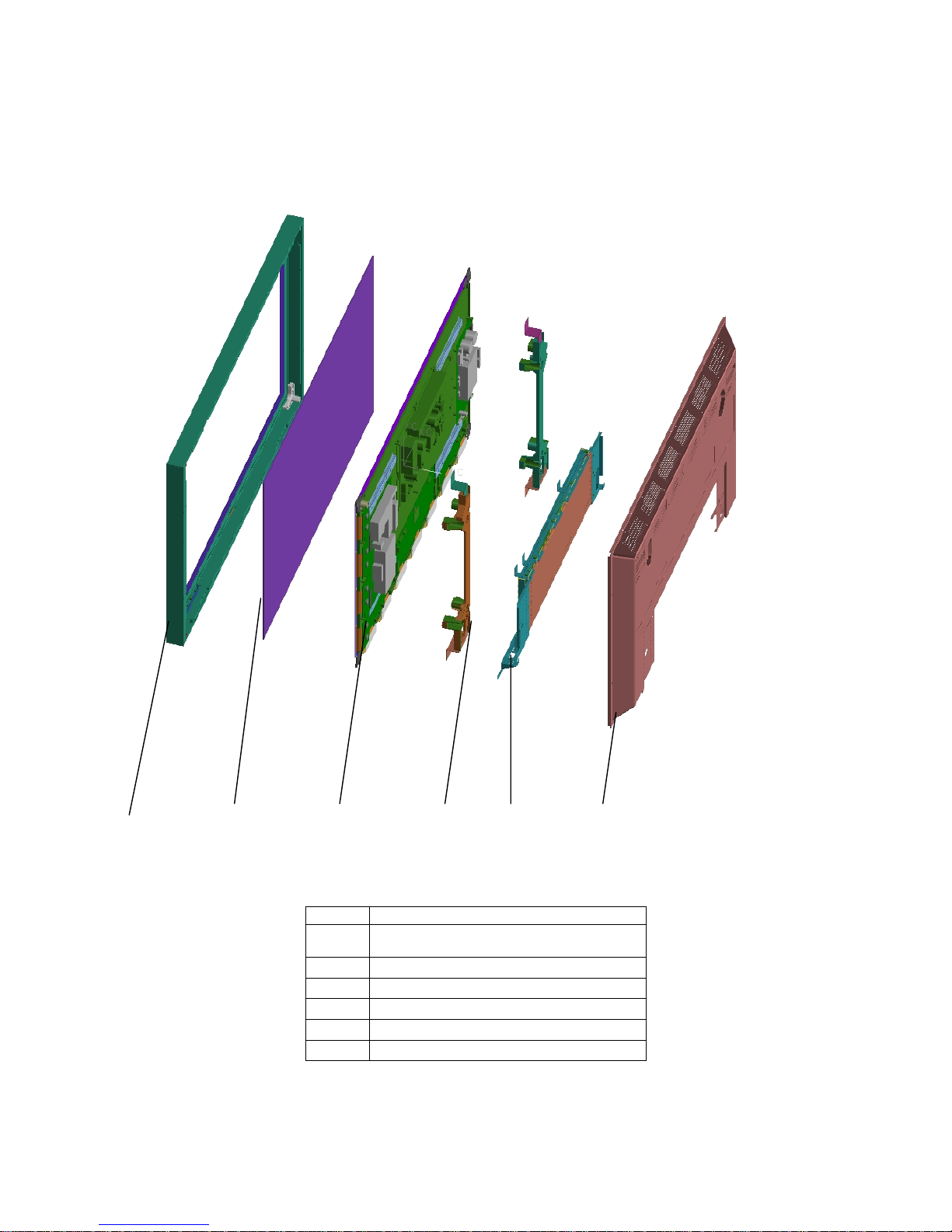
3.1 PDP Inside Drawing:
1 2 3 4 5 6
No. Name
①
Front Cabinet
②
Filter Glass
③
PDP Panel Module
④
Shelve Bar
⑤
Down Cover Module etc.
⑥
Back Cabinet
5
Remarks: This drawing is for references only, please see the main assembly diagram and wire-connecting diagram for
details.
3.2
Circuit block diagram:
PS08 chassis PDPD TV is mainly composed of regulator circuit、RF circuit、video processor circuit、Power Amplify
circuit、Analog Video circuit、System Control circuit and Key Control circuit, block diagram of unit circuit is below:
Power Board
AV Board
TDA8759
FLASH
+6V
+5VS
+12V
+32V
IF
CVBS
Analog
24bit
ITU-R656
Main Board
Panel
L V D S
GM1601
SAA7115
HDTV
SubTuner
DVI
PC
UOCIII
Main
Tuner
k Panel
IR
Panel
Control Signal
B
G
R
B
G
R
Audio
Speaker
TA2024
audio amplify board
+3.3V
+12VAU
3.3 PCB assembly introduction
It is mainly composed of AV Board、Remote Control Receiving board 、K Board 、power board、power amplifier
board and Main Board. Herein introduct function of each PCB module:
Number Parts Description
1 Main Board
assembly
It is the core of signal processing for PDP TV, which takes responsibility of transforming
outer signal into the uniform digital signal identified by PDP display with control of
System circuit. TV, AV and S-video signals input from AV Board are decoded by
UOCIII to output RGB signal ,A/D converted by TDA8759,output 24bit RGB digital
signal, then it is processed by GM1601/GM1501 to accomplish format convert, produce
LVDS signal displayed on the screen. In addition, signals input from VGA、DVI
would directly enter into GM1501 to process 、format convert and on screen display.
2 AV Board
assembly
It is mainly composed of two tuners (main and sub tuners) 、earphone output and some
peripheral processing circuit. The main tuner demodulates RF signal to IF signal, and
the sub tuner produces CVBS signal, all signals are sent to the main board to do
corresponding process after transfer .Earphone jack can connect earphone output directly,
and output volume can be adjusted.
6
3 Remote Control
Receiving
assembly
It is composed of one indicator lamp, buzzer and one remote control receiving head,
which enable Users operate the TV conveniently and know its current working status
simply with a remote control box. Indicator lamp indicates unit on/off status and buzz
prompts validity of key operation.
4 Built-in Power
Board
assembly
It can transform AC 220V into multiple DC power, including +12VAU(audio power
amplifier),+12V,+A6V,+D6V,+D3.3V,+34V and +5VS standby power supply .
5 K Board
module
It consists of 7 inductive buttons by which users can operate the TV freely.
6 Power amplifier
board assembly
Audio adopts two channel T-class digital audio power amplifier IC. Left and right channel
output 2X5W.
7 Screen
assembly
PDP panel is used to display image signal processed by main board.
8 Transfer board
assembly(only
used LG panel)
Transform each kind of DC voltage from panel(+9V、 +12V、24V) into each kind of DC
voltage used by main board(+3.3、+D6V、A6V、+34V、+12V、+12VAU).
7
PartⅡ:Introduction on main components functions of PT4216
1、PT4216 main components and function
NO. NAME TYPE
Function
AV board assembly
1 UT921 TMI4-C22P2RW Output sub-picture CVBS signal
2 UT920 TAD5-C2IP1RW Output sound and video IF signal
Main board assembly
3 U901 PIC16F505 Standby control CPU
4
U302,U303
24LC21A T/SN EEPROM
5 U701 24LC32A T/SN buffer
6 U306,U307,UA3 FSAV330QSCX Select switch
7 K201 K7262N SAW filter
8 K202 K9352N SAW filter
9 U801 AM29LV800DT-70EC
Flash,save unit control program
10 U700 GM1501-BD Video processor
11 U201 TDA15063H-N1B06557
Video and audio decoder
12 U402 SAA7115HL/V1 Sub-channel video decoder
13 U305 SM5302AS-G-ET High definition signal filter
14 U400 TDA8759HV/8/C1 Video signal A/D converter
15 U5 TDA9178T/N1 Video signal picture quality improvement
16 U600
MT46V2M32LG-4
Frame buffer
2、PDP TV PT4216 main components function introduction:
2.1 Main tuner(TAD5-C2IP1RW)
Pin number Pin definition Pin function description
1 AGC Auto gain control
2 UT Not connect
3 ADD Ground
4 SCL IIC bus(clock)
5 SDA IIC bus(data)
6 NC Not connect
7 +5V Power
8 NC Not connect
9 30V Form 0~30V tune voltage
10 NC Not connect
11 IF Output IF TV signal
2.2 Sub tuner(TMI4-C22P2RW):
Pin number Pin definition Pin function description
1 AGC Auto gain control
2 NC Not connect
3 ADD Ground
4 SCL IIC bus(clock)
5 SDA IIC bus(data)
6 NC Not connect
7 +5V Power
8 NC Not connect
9 33V Form 0~33V tune voltage
10 NC Not connect
11 IF IF signal output(not connect)
8
12 IF IF signal output(not connect)
13 SW0 Band control
14 SW1 Band control
15 NC Not connect
16 SIF Not connect
17 AGC Auto gain control
18 VEDIO CVBS signal output
19 +5V Power
20 AUDIO Not connect
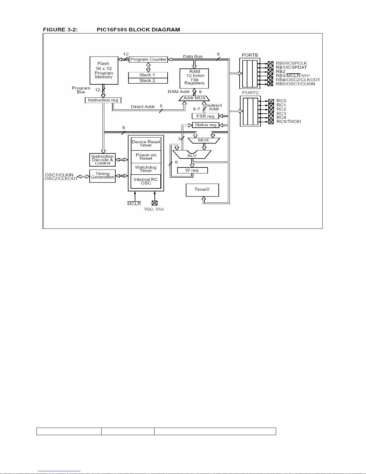
2.3、Standby control CPU(PIC16F505)
Pin number Pin definition Pin function description
1
VDD(+3.3V)
Power
2 RB5/OSC1/CLCKIN NC
3 RB4/OSC2/CLCKOUT LED1 KEYPAD STB output, standby indicator lamp control
4 RB3/MCLP/VPP Input voltage (+5V)when programming or reset input(+5V)
5 RC5 I/O port: POWER OFF1 input, from GM1501 output, inform
PIC16F505 to do off operation.
6 RC4 I/O port: ALARM input, turn on on time enable control.
7 RC3 I/O port: PDP-STB output, standby/on control
8 RC2 I/O port: POWER-STANDBY output,GM1501 to inform
executing off operation by key button.
9 RC1 I/O port: IRIN remote instruction input
10 RC0 I/O port: POWERKEY input, connect to on/off key of k board
directly.
11 RB2 I/O port: connect +3.3V
12 RB1/ICSPCLK programming use
13 RB0/ICSPDAT programming use
14 VSS Ground
9
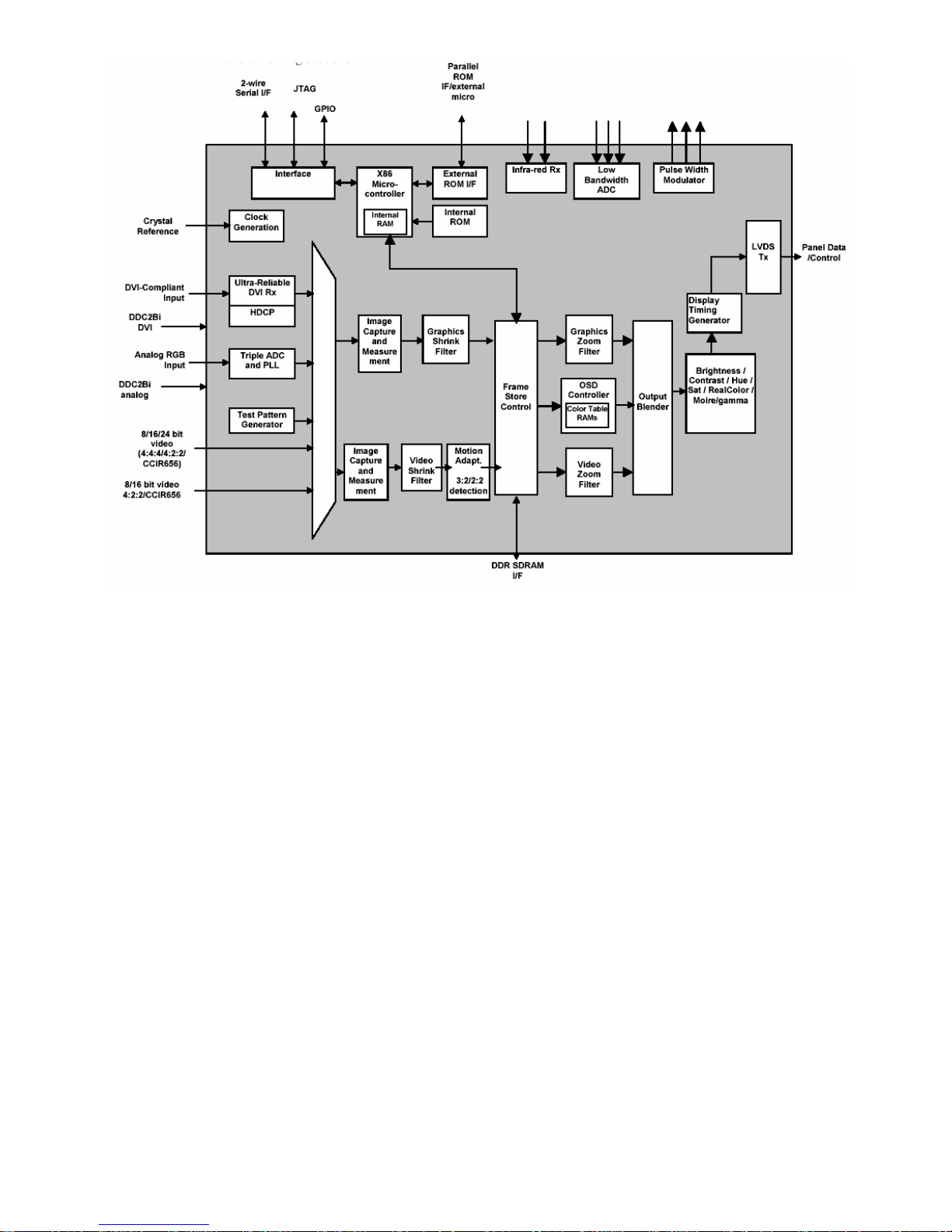
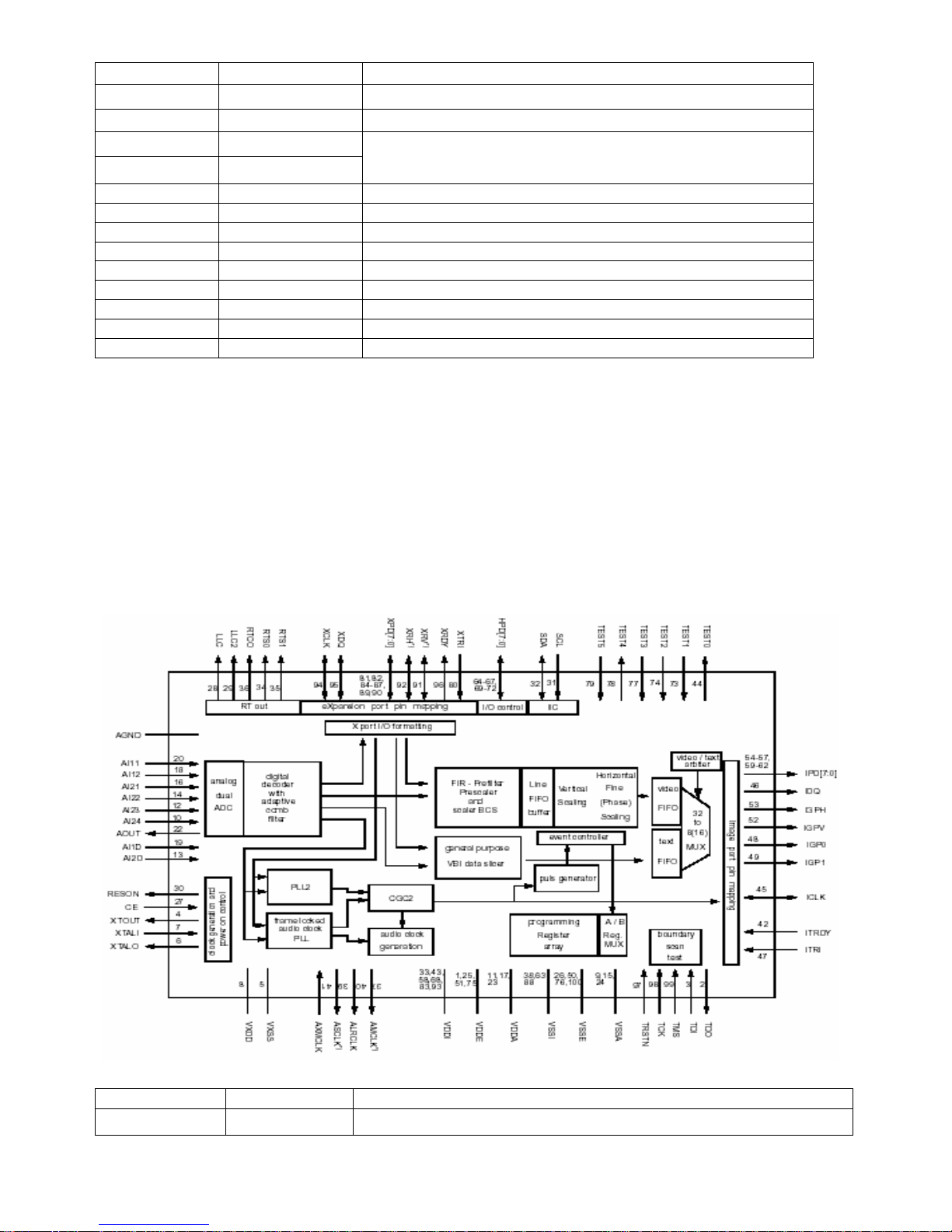
2.4 GM1501
GM1501 is a kind of dual channels image and video processing chip, which is mainly used for LCD displays and TV
integrated products. With the resolution of WUXGA, it not only supports PIP technology, but also include all IC function
of picture snap, process and display clock control. It integrates high speed AD converter, PLL, high reliability DVI
receiver , X86 series microprocessor and LVDS converter inside. Its main e feature as below:
● High quality image zoom function
● Analog RGB signal input interface
● Intelligent input signal mode auto identification;
● Integrated high performance PLL output
● High-reliable self-adaptive DVI input interface;
●4:4:4/4:2:2/CCR656/601 8/16/24bit digital video interface;;
● Embedded adjustment circuit for gain、contrast、brightness、color saturation、hue and skin color;
● technology of reducing EMI power consumption efficiently;
●small angle oblique ripple process;
● High quality video process technology;
● Programmable output format;
● Embedded LVDS transmitter;
● Advanced OSD;
● Embedded micro controller
Pin Description:
Pin Name Description
10
Analog signal input port
L3 AVSYNC ADC vertical synchronization signal input
L4 AHSYNC ADC horizontal synchronization signal input
N2 VGA-SCL VGA lock input
N1 VGA-SDA VGA digital input
D1、D2 RED+、RED-
Red analog signal input
C3 SOG Green pedestal synchronization signal
C1、C2 GREEN+、-
Green analog signal input
B1、B2 BLUE+、BLUE-
Blue analog signal input
A2,B3,E3,D3 ADC3.3 ADC3.3Vpower supply
A3,A4
ADC1.8 ADC1.8Vpower supply
A5,B4
ADC-DGND ADC digital ground
C4,D4,E1,E2,E4
ADC-AGND ADC analog ground
DVI import port
N4
DVI-SCL
DDC interface , serial clock signal
N3
DVI-SDA
DDC interface ,serial data signal
A6,B6 RXC+,RXC-
DVI clock input signal
A8~A10
B8~B10
RX0+~RX2+
RX0-~RX2-
DVI input port
B11 REXT External interrupt resistance
C6~C11
DVI-3.3 DVI 3.3V power supply
D6、D8~D10
DVI-1.8 DVI 1.8V power supply
A7,A11,B5,B7,C7,D7
D11
DVI-GND DVI ground
Low bandwidth ADC port
C13 LBADC-33 ADC3.3Vpower supply
A12,B12,C12 LBADC_IN1~
LBADC_IN3
ADC analog input channel
D12 LBADC_RETURN Channel analog ground
D13 LBADC-GND Power supply voltage analog ground
OCM bus port
AA1~AA3,Y1~Y3,
W1~W3,V1~V4,
U1~U4,T1~T3
OCMADDR0~
OCMADDR19
Address input output port
AB1~AB3,AC1~AC3,
AD1~AD4,AE1~AE3,
AF1~AF3
OCMDATA0~
OCMDATA15
Data input output port
OCM port control signal
R1,T4,P1,P2
ROM_CSn~
ROM_CS2n
chip selection signal
R2 OCM_REn Read enable signal
R3 OCM_WEn Write enable signal
L1
L2
OCM_INT2
OCM_INT1
Interrupt
M1 OCM_UDO OCM data output
M2 OCM_UDI OCM data input
D25 OCM_TIMER1 OCM timer input
Standard definition video control port
D16 SVCLK SV pixels clock input
C14 SVHSYNC SV horizon synchronization signal input
B14 SVVSYNC SV vertical synchronization signal input
A14 SVODD Scan status input
A17 SVDV SV data input
Standard definition video data port
D14,D15,A15,A16,
B15,B16,C15,C16
SVDATA7~
SVDATA0
SV ITU656 data input
11
Video Control Port
A20 VCLK Video pixels clock signal
D19 VHS_CSYNC Video horizonl synchronization signal input
C20 VVS Video vertical synchronization signal input
B20 VODD Scan status input
D20 VDV (VSOG) Video data input
B17 VCLAMP Video clamp enable output
A21,A22,A23,B21,
B22,C21,C22,D21
VGRN7~ VGRN0 Green pedestal signal or Y signal input
C17,C18,C19,A18
A19,B18,B19,D18
VRED7~ VRED0
Red pedestal signal or V/Cr/Pr signal input
B23,B24,B25,A24
A25,C23,C24,D24
VBLU7~ VBLU0
Blue pedestal signal or U/Cb/Pb signal input
Screen Control Port
A26 PPWR Screen power control
B26 PBIAS Screen bias control
D26,C25,C26
PWM2 ~PWM0 Pulse width modulation output
AC7 DCLK Pixels clock output
AC16 OEXTR Connect external LVDS bias resistance
LVDS Port
AE14~AE16,AE19~
AE23,AF13~AF16
AF19~AF23,AF11
A0-~A3-, A0+~A3+
B0-~B3-, B0+~B3+
Low voltage difference data input
AD14,AD11,AE13
AE11,AC11,AF10
LVDS_SHIELD[5] ~
LVDS_SHIELD[0]
Low voltage difference protect output
AE12,AF12,
AF20,AE20
AC+,AC-,BC+,BC- Low voltage difference protect input
Screen Port Power Supply
AD12,AD13,AC12 LVDSB_3.3 LVDS B channel power supply
AC13,AC14,AC15 LVDSB_GND B channel ground
AC20,AC21,AC22 LVDSA_3.3 LVDS A channel power supply
AD19,AC19,AC20 LVDSA_GND A channel ground
AE17 VDDD33_LVDS Analog power supply
AD17 VSSD33_LVDS Analog ground
Clock Composite and Power Supply
G4 XTAL Crystal oscillator interface
F2
VDDD33_PLL,
H1 VDDD33_SDDS
J1 VDDD33_DDDS
Digital power supply
G2 VSSD33_PLL
J4 VSSD33_SDDS
K4 VSSD33_DDDS
Digital ground
F4 VDDA33_RPLL
G1 VDDA33_FPLL
H3 VDDA33_SDDS
J3 VDDA33_DDDS
Analog power supply
F3 VSSA33_RPLL
H4 VSSA33_FPLL
H2 VSSA33_DDDS
J2 VSSA33_DDDS
Analog ground
G3 TCLK Reference clock signal input
K2 ACS_RSET_HD External resistance terminal
System Signal
12
K1 RESETn Reset signal
M3,M4 IR0,IR1
P4 MSTR_SCL Master clock output signal
P3 MSTR_SDA Master data output/input signal
R4 EXTCLK External clock input
Frame memory interface
U24,U23 FSCLKp,FSCLKn Differential store clock output
V24,V25 FSRAS,FSCAS Address output
V26 FSWE Write enable terminal
W26 FSCKE Read enable terminal
J24 FSVREF Reference voltage input
K26 FSVREFVSS Reference voltage ground
W25 FSVREF Reference voltage input
W24 FSVREFVSS Reference voltage ground
L26 FSDQS Data filter
F24~F26,G23~G26
H24~H26,J25,J26,
R24~R26,P24~P26
N23~N26,…….
FSDATA31~
FSDATA0
Data input output port
T24,T25,U25,U26 FSDQM3~ FSDQM0 Data output mark
Y26
Y25
FSBKSEL1
,
FSBKSEL0
Layer select address
AA24~AA26
AB24~AB26,
AC24~AC26
AD24~AD26
FSADDR11~
FSADDR0
Row and column address output
E23, F23, H23, J23,
L23,M23,P23, R23,
T23,V23,W23,Y23,
AA23,AB23,AC23
FS_2.5
2.5V power supply
K23 VDDA18_DLL 1.8V power supply
K25 VSSA18_DLL Power supply ground
Digital power
K10,K11,K16,K17,
L11,L16,T11,T16,
T17,U10,U11,U16,U17
CORE_1.8 1.8V power supply
D23, W4,Y4, AA4,
AB4,AC4,AC6,D17,
D22,AC8,AC10
IO_3.3
3.3V power supply
K12,K13,K14,K15,
L10,L12,L13,L14,
L15,L17,M10,M11,
M12,M13。。。。。。
D_GND
Power ground
A1,AC,D5,AC17,
K3,F1
NO_CONNECT
NC
GM1501internal block Diagram:
13
2.5. Brief Introduction of TDA8759:
TDA8759 is a triple 8-bit video converter interface. Sample rate is up to 81 Mbps .The IC can convert analog RGB
signal into a 24bit RGB digital signal o, or converts analog YUV or YCbCr signal into a YUV or RGB digital.
The IC supports resolutions from 480i and VGA to HDTV and XGA.
● Triple 8-bit Analog-to-Digital Converter (ADC)
●Three independent I2C selectable analog video sources
●Auto detect to interlace scan video signal
●1.8Vand 3.3Vsupplies
● Low gain temperature shift
●Output format support RGB 4:4:4, YUV 4:4:4, YUV 4:2:2 ,CCIR 656 or YUV 4:2:2 ;
●I²C bus control
●Programmable clock phase correct circuit inside
●100 MHz Amplifier bandwidth
●Integrated PLL distribution
●Power-Down mode
TDA8759 internal schematic Diagram:
14
Pin Description:
Pin Name Description
1 HREF Horizon reference output
2 VCLK Video clock output
3,13,21,29,
37,45,164
VDDO Video port output supply voltage
4,14,22,30
38,46,165
OGND Video port output ground
7,8,9,10,
15,16,17,18
VPA0~VPA7 Video port A
11,116,130,132 VDDC Power supply port
12,117,159 CGND Ground
23~28,31,32 VPB0~VPB7 Video port B
35,36,39~44 VPC0~VPC7 Video port C
47,53,57,58,55
60,66,70,71,75
81,83,85,86,
AGND Analog ground
48,54,59,61,67
69,76,82,85,87,88
VDDA Power supply port
49 REFB/Pb Blue/blue-chrominance channel reference input signal
52,51,50 B/Pb1~ B/Pb3 Blue/blue-chrominance channel analog input
56 BIAS Bias input
62 REFG/Y Green/luminance reference input
15
65,64,63 G/Y1~G/Y3 Green/luminance analog input
74,73,72 SOG/Y1~SOG/Y3 Sync on green//luminance input
77 REFR/Pr Red/red-chrominance channel reference input
80,79,78 R/Pr1~ R/Pr3 Red/red-chrominance channel analog input
89~92,97~101
112,121,122,
124,125,160~163
TST0~TST17 Reserved for test
93 PD Power-down control input
94 OE Output enable signal input
96 A0 I²C bus address control signal input
102 COAST PLL control signal input
103 GAIN Gain input
104 CLAMP Clamp input
105~107 VSYNC1~VSYNC3 Vertical synchronization signal input
108~110 H(C)SYNC1~
H(C)SYNC3
Horizon (color)synchronization signal input
111 CKEXT External clock input
113 TCLK Reserved for test
114 DIS I²C bus disable control signal input
118 SDA I²C bus data input/output
119 SCL I²C bus clock input
120,126,127,131
133,142,148,
IGND Input digital ground
123,138,139,145
151,157
VDDI Input digital supply voltage
166 PL PLL disable signal output
167 DE Data enable output
168 HS Horizon synchronization signal input
169 VS vertical synchronization signal input
170 CS Color synchronization signal output
171 ORR/V Red / chrominance ADC output
172 ORB/U Blue /chrominance ADC output
173 ORG/Y Green / chrominance ADC output
174 VAI Video dynamic indication output
175 FREF Scan signal output
17 VREF Vertical reference input
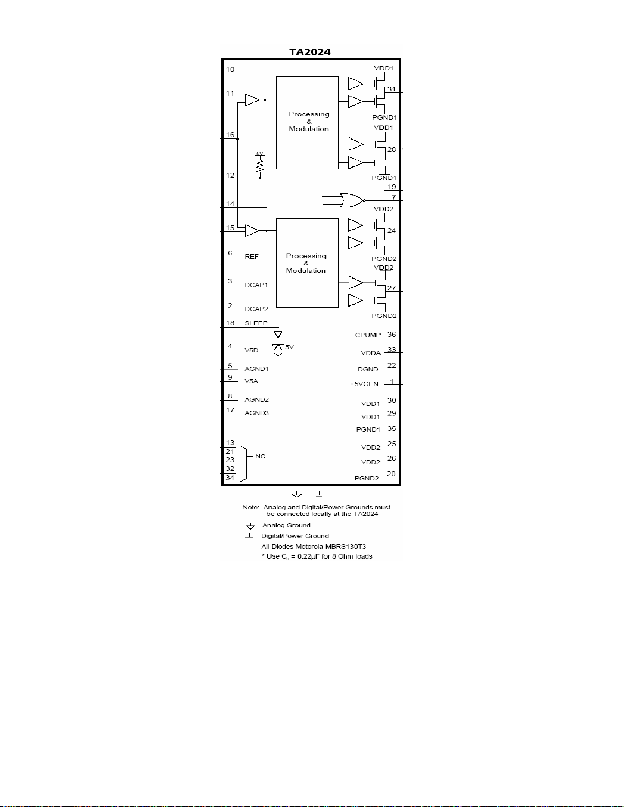
2. 6、TA2024 general:
The TA2024 is a 10W/ch continuous average two-channel Class-T Digital Audio Power Amplifier IC using
Tripath’s proprietary Digital Power Processing™ technology. Class-T amplifiers offer both the audio fidelity of
Class-AB and the power efficiency of Class-D amplifiers. It has below feature:
z Mute control
z Temperature protect circuit
z Low noise switch
z Power supply:12V
Pin Function Descriptions:
Pin(s) Name Function
2, 3 DCAP2, DCAP1 Charge pump switching pins
4, 9 V5D, V5A Digital 5VDC, Analog 5VDC
5, 8, 17 AGND1, AGND2, AGND3 Analog Ground
6 REF Internal reference voltage
16
7 OVERLOADB A logic low output indicates the input signal
has overloaded the amplifier
10,14
OAOUT1, OAOUT2 Input stage output pins.
11, 15 INV1, INV2 Single-ended inputs
12 MUTE Mute control
16 BIASCAP Input stage bias voltage
18 SLEEP Sleep mode control
19 FAULT A logic high output indicates thermal
overload
20, 35 PGND2, PGND1 Power Grounds (high current)
22 DGND Digital Ground
24, 27; 31, 28 OUTP2 & OUTM2; OUTP1
& OUTM1
Bridged outputs
25, 26, 29, 30
VDD2, VDD2 , VDD1,
VDD1
Supply pins for high current H-bridges,
nominally 12VDC.
13, 21, 23, 32, 34 NC Not connected
33 VDDA Analog 12VDC
36 CPUMP Charge pump output
1 5VGEN Regulated 5VDC source used to supply
power to the input section (pins 4 and 9).
TA2024 Block Diagram:
17
2.7.Brief Introduction to SM5302AS :
The SM5302AS is a 3-channel video buffer with built-in 5
th -
order low pass filter. The cutoff frequency, signal input
type, and output gain switching can be controlled using a IIC control bus, and the IIC slave address can be set by ADS(3-state
input) to allow a maximum of three devices to be used simultaneous.
FEATUES:
● supply voltage:analog:4.75V~5.25V; digital:3.0~5.5V
● 2-system input multiplexer function(switchable using IIC or MUXSEL input)
● Filter bypass mode function for display specifications up to SVGA resolution.
●
Video input pins can be independently set to sync-tip clamp/bias/direct input.
● Output gain switching: 0/6dB
● Output sag compensation circuit built-in.
●
Half fc mode switch function(CH-2,CH-3) suitable for digital component signals.

18
● IIC interface control: slave address:90h,92h or 94h(up to three devices can be used simultaneously,selected by ADS
input); data transfer rate: fast mode(up to 400kbps)
● Cutoff frequency:4.8 to 43MHz variable
SM5302AS Internal Diagram:
Pin Description:
Pin Name Description
1 REF1 Internal reference voltage 1
2 VDD
3 SDA
Digital supply(3.0~5.5V).
IIC data signal input/output
4 SCL
5 Vss
IIC clock signal input
Digital ground
6 MUXSEL Input multiplexer switch control
7 ADS IIC slave address select(three state input)
8 IN1A Video signal input 1(CH-1, input A)
9 IN1B Video signal input 1(CH-1, input B)
10 ISET
Internal current-setting resistor(Riset) connection(1.8K
Ω)
11 IN2A Video signal input 1(CH-2, input A)
12 IN2B Video signal input 1(CH-2, input B)
13 IN3A Video signal input 1(CH-3, input A)
14 IN3B Video signal input 1(CH-3, input B)
19
15 GND3 Analog ground(CH-3)
16 Out3B Video signal output(CH-3,for sag compensation)
17 Out3A Video signal output(CH-3)
18 VCC3
19 GND2
Analog supply(CH-3)(4.75 to 5.25V).
Analog ground(CH-2)
20 Out2B Video signal output(CH-2,for sag compensation)
21 Out2A Video signal output(CH-2)
22 VCC2 Analog supply(CH-2)(4.75 to 5.25V).
23 GND1 Analog ground(CH-1, Vref)
24 Out1B Video signal output(CH-1,for sag compensation)
25 Out1A Video signal output(CH-1)
26 VCC1 Analog supply(CH-1,Vref)(4.75 to 5.25V).
27 REF3 Internal reference voltage 3
28 REF2 Internal reference voltage 2
2.8. Brief Introduction to SAA7115:
The SAA7115 is a video capture device for various applications ranging from small screen products like e.g. digital set top
boxes, personal video recording applications to big screen devices like e.g. LCD projectors due to it’s improved comb filter
performance and 10 bit video output capabilities.
●Six analog inputs, internal analog source selectors;
●Two improved 9 Bit CMOS analog-to-digital converter in differential CMOS style;
●
Automatic Clamp Control (ACC) for CVBS, Y and C;
●Enhanced Horizontal and vertical Sync Detection;
●
PAL delay line for correcting PAL phase errors;
●
Automatic TV/VCR detection;
SAA7115 Internal Diagram:
Pin Function:
Pin Name Description
1,8,11,17,23,25,33 VDD Supply voltage port
 Loading...