

Changhong Electric MSD308PX, MSD309PX Maintenance Manual

0
LCD COLOUR TV
MAINTENANCE MANUAL
MODEL: LS18 CHASSIS(MSD308/309PX)
Please r e ad this manual carefully before maintenance

1
CATALOG
Chapter1 Safety and notes ......................................................................................................................................................... 2
1-1 Installation notes ......................................................................................................................................................... 2
1-2 Attention points of operation and using ...................................................................................................................... 2
1-3 Storage notes ............................................................................................................................................................... 2
1-4 Dismantling notes ........................................................................................................................................................ 2
1-5 High-voltage warning .................................................................................................................................................. 3
Chapter2 hole machine standard and terminal functions ........................................................................................................... 3
2-1 Basic standard ............................................................................................................................................................. 3
2-2 Introduction of terminals(practicality photos) ............................................................................................................. 4
Chapter3 Main chip functions and the introductions of power supply ...................................................................................... 5
3-1 Main IC and functions of LS18 ................................................................................................................................... 5
3-2 Pin function description of LS18 chip ......................................................................................................................... 7
3-2-1 MSD308PX recommended operating power conditons ................................................................................... 7
3-2-2 Pin function of DTI1-E4I1VH tuner ................................................................................................................ 7
3-2-3 EN25Q64-104HIP brief introduction: .............................................................................................................. 7
3-2-4 74HC4052 brief introduction: .......................................................................................................................... 7
3-2-5 SGM330 brief introduction: ............................................................................................................................. 8
3.3 Brief introduction of power supply.............................................................................................................................. 8
Chapter4 The chassis frame diagram, mainboard power supply systems, mainboard interface definition and the waveform
of key points .............................................................................................................................................................................. 9
4-1 The chassis frame diagram .......................................................................................................................................... 9
4-2 Power supply system ................................................................................................................................................... 9
4-2-1 The composition and distribution of the TV power supply .............................................................................. 9
4-2-2 Pin voltage of the voltage adjustor on the mainboard .................................................................................... 10
4-2-3 Interface definition ......................................................................................................................................... 11
4-3 The waveform of key points ...................................................................................................................................... 12
Chapter5 Software upgrade instructions .................................................................................................................................. 13
5-1 Software upgrade tooling---there are two kinds of using upgrade tooling ................................................................ 13
5-2 Software upgrade introduction .................................................................................................................................. 13
Chapter6: Classical accident maintenance procedures and examples ..................................................................................... 18
6-1 The thinking of don’t boot ......................................................................................................................................... 18
6-2 Common problems for your reference ...................................................................................................................... 18
Chapter7 High voltage and high current wearing parts list ..................................................................................................... 19
Chapter8 Factory mode parameter setting instructions and notes ........................................................................................... 20
8-1 Enter into the factory mode ....................................................................................................................................... 20
8-2 Setting method of factory menu ................................................................................................................................ 21
Chapter9 Instructions of LS18 module Circuit Schematic Diagram ....................................................................................... 22
Appendix : Circuit Schematic Diagram .............................................................................................................................. 25
2
Chapter1 Safety and notes
1-1 Installation notes
(1) Please don't beat or rub, scratch the surface of the LCD s creen heavil y, don’t touch it with your hand
casually.
(2) When the screen is dirty, please clean it with absorbent cotton or cotton cloth slightly.
(3) Please clean it timely when water or other viscosity pollution fall, which may make the LCD face or
color change.
(4) Please don’t make the LCD screen shaked by strong external force.
1-2 Attention points of operation and using
(1) Please unplug the power cable before moving the LCD screen.
(2) Please don’t change the original setting of the mainboard’s, if not, the brightness and white balance etc.
may not meet the specification.
(3) The radiation of a long time using in the room temperature is larger than the low temperature.
(4) Please note that the long displaying image may remain at the top when shutdown the machine.
(5) Please avoid the impact from the mobile phone to protect your TV.
1-3 Storage notes
(1)When stored for a long time, please keep t he temperature between 0℃to 40℃,don’t expose the TV to
the strong sunlight, the humidity should be less than 85%RH.
(2)Please don’t put your TV under high humidity and high temperature environment, for example, the
temperature: 60℃, and the humidity: 85%RH.
(3)Please don’t put your TV under low temperature environment, for exam ple, the tempe rature l ower th an
-25℃.
1-4 Dismantling notes
(1)As LCD screen is easy to be damaged, while dismantle, please attention to protect.
(2)Please attenti on the position of each screw w hen dismantle, in cas e to beat the wrong position when
install, if not, it may lead to crack or slide of the face frame.
(3) If you need to dismantle t he power board or the mainboard, p lease att ention th e position and direction
of each line, especi ally the direction of t he screen line, in case of causin g accident when install. Before
3
dismantle, we can take some photos of the line route for the comparison of installing.
(4)After check and maintenance, please assure that there is no foreign body in the machine when install.
1-5 High-voltage war nin g
The high-voltage of the LCD screen is generated by the power supply step-up board, without attention to
exposure to the high voltage, one may meet a serious electricity shock.
Chapter2 hole machine standard and terminal functions
2-1 Basic standard
Item Standard
LCD Panel
visual area
32” inches(opposite angles) (BOE)
the parameters are for
reference only,the specific
should accord to the standard
of the screen practicality of
the batch orders
aspect ratio 16:9
resolving ratio 1366 x768
visual area H x V 697.68m m (H) ×392.25m m (V)
display colour 16.7 million
contrast
4000:1
brightness 450cd/m²
visual angle 178°(horizontal)/178° (vertical)
react time 8ms
backlight life 50000 hours
color temperature cold/hot
TV function
sound system
B/G、D/K、I、M
color system PAL / SECAM / NTSC
A
udio and video
signal input
AV AV x 2
Audio L/R x 1
S-Video S-Video x 1
aberration signal YPbPr x 2
support to1080P ,Audio L/R x 1,
HDMI HDMI x3 support to1080P
PC input
plug and use
input frequency
H: 31.5K -50KHz
V: 60Hz to 75Hz
recommend 1024x768(60HZ)
Video output Output CVBS signal
Output TV and AV signal ,
Audio L/R x
1
Audio output Audio output L / R 10W inner speakers for each channel
4
Power power supply AC100V~240V, 50/60Hz
power achievement <150W
requirement for environment
operation temperature
storage temperature
operation humidity
+ 0° ~ + 40° ,
- 20 ° ~ + 60°
10% ~ 85%
appearance size W x H x D
net weight no accessory Kg
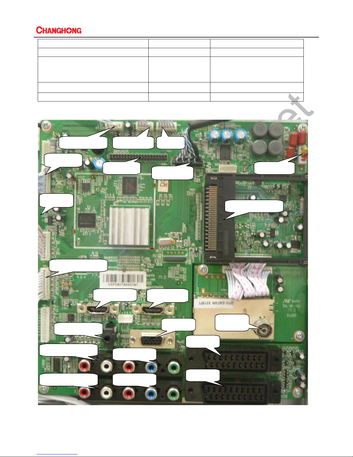
2-2 Introduction of terminals(practicality photos)
YpbPr2 audio input
SCART1
SCART2
HDMI1 input
PC input
RF input
YpbPr1 input
PC audio input
YpbPr1 audio input
HDMI2 input
PCMCIA Card Slot
YpbPr2 input
Side AV inputinput
HDMI3 input
Keypad input IR input Backlight on/off
Audio output Lvds output
Usb input
Power input
5
ATTENTION:
1.HDMI and YPbPr support to 1080P;
2.The recommendation resolving ratio of PC is 1024X768;
3.Side AV input must use a small board.
Chapter3 Main chip functions and the introductions of power supply
3-1 Main IC and functions of LS18
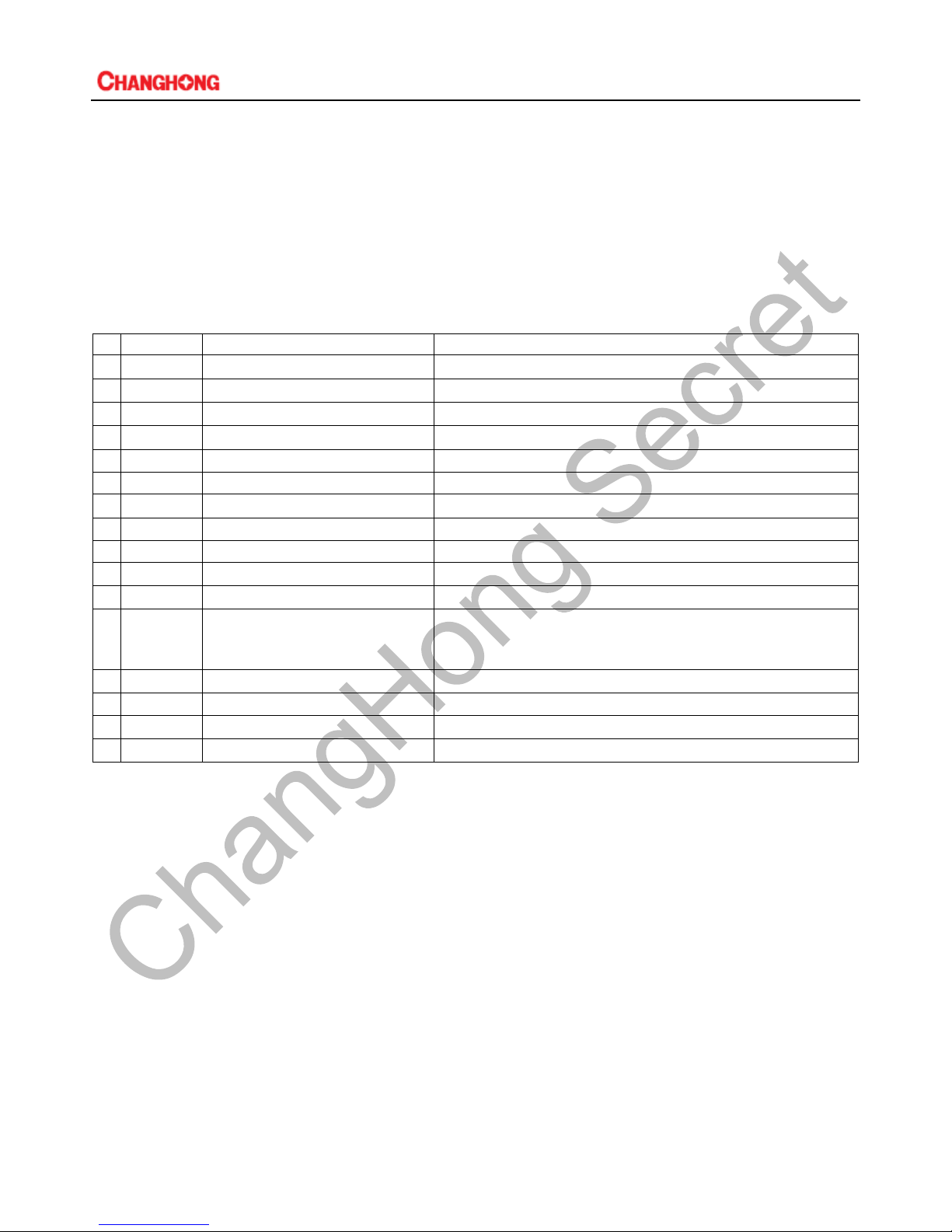
No. Item no. Model Main function
1 U21 DTI1-E4I1VH(JUB2.891.170) Tuner output IF signal
2 U2 MSD308PX Video decoder, image processor, A/D and D/A conversion
3 U4
AT24C04BN-SH-T
Store HDCP key
4 U52
AO4459
Power switch
5
U9,U15
W9751G6IB-25 DDR
6 U24 EN25Q64-104HIP Store program
7
U37,U38
LR1117/A-3.3 5V to 3.3V LDO
8 U39 LR1117/A-1.8 5V to 1.8V LDO
9 U36
LR1117/A-2.5
5V to 2.5V LDO
10 U51 AP1534SG13 5V to1.32V DC to DC
11 U18
AS7805DTR-E1
12V to 5V LDO
12
U17,U19
PT2328-X-TP$PI5V330AQ$
PI5V330AQX$SGM330A-YQS
$CS43V30
Video Switch
13 U11 STA335BW Audio amplifier
14 U20 SN74LV4052 Audio switch
15 U53
AO4803A
USB power switch
16 U30 HDBF36A8Dc SAW filter
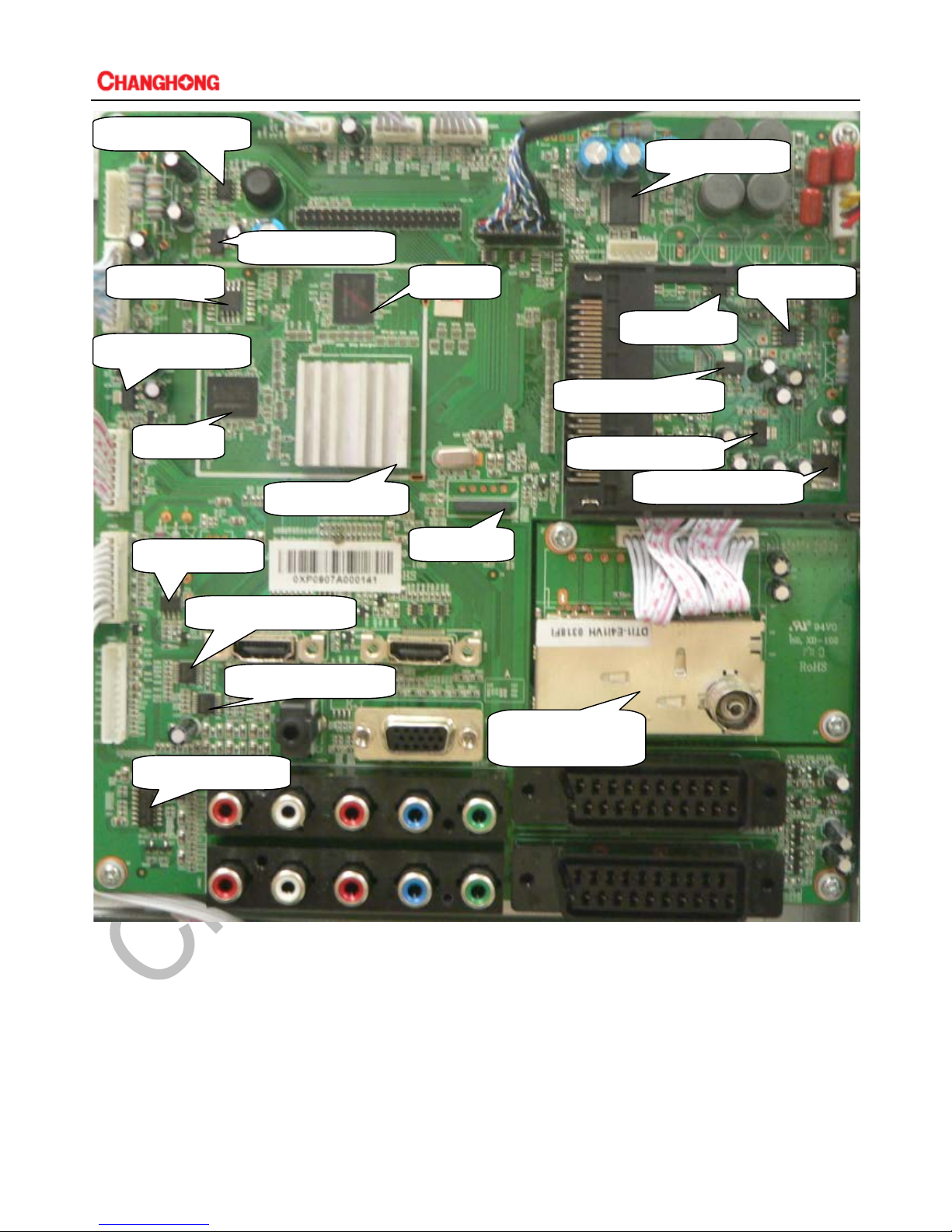
6
U4:EEPROM
U2: MSD308PX
U9:DDR
U24:FLASH U52: AO4459
U39: LR1117/A-1.8
U37: LR1117/A-3.3
U20: SN74LV4052
U18: AS7805DTR-E1
U36: LR1117/A-2.5
U51: AP1534SG13
U11: STA335BW
U10: DTI1-E4I1VH
(JUB2.891.170)
U15:DDR
U38: LR1117/A-3.3
U53: AO4803A
U19: SGM330A-YQS
U17: SGM330A-YQS
U30: SAW
7
3-2 Pin function description of LS18 chip
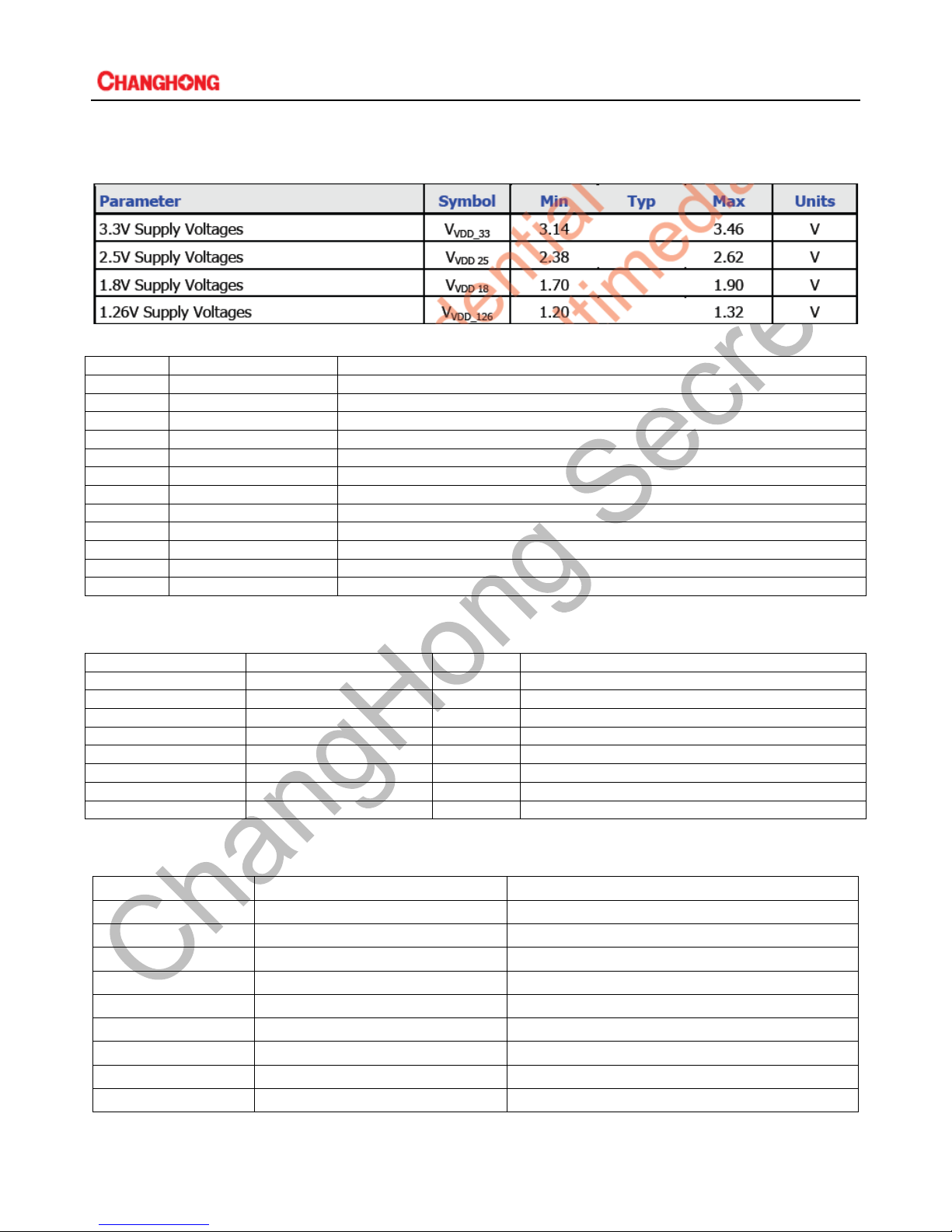
3-2-1 MSD308PX recommended operating power conditons
3-2-2 Pin function of DTI1-E4I1VH tuner
PIN
SYMBOL
Description
1
NC
Not connect
2
VCC2
+5V POWER
3
RF-AGC
RF-AGC monitor(Not connect)
4
SCL
I2C Serial Clock
5
SDA
I2C Serial DATA
6
VCC3
+5V POWER
7
TU
Tuning voltage monitor(Not connect)
8
AS
Address
9
IF-AGC
IF AGC Control V oltage
10
DIF1
High level IF output1
11
DIF2
High level IF output1
12
AIF
Analog IF output
3-2-3 EN25Q64-104HIP brief introduction:
Pin introduction:
Pin NO.
Pin Name
I/O
Function
1
CS# I Chip Select
2
DO O Serial Data Output
3
WP#
I
White Protect
4
Vss Ground
5
DI
I/O
Serial Data Input
6
CLK
I
Serial Clock
7
NC I Not Connect
8
VCC
Power Supply
3-2-4 74HC4052 brief introduction:
Pin introduction:
Pin SYMBOL Function description
1,5,2,4 2Y0 to 2Y3 Independent Input Outputs
6 INH INHIBIT In p u t
7 VEE Negative Supply Voltage
10,9 A,B Select Inputs
12,14,15,11 1Y0 to 1Y3 Independent Input Outputs
3 2-COM Common X Output/Input
13 1-COM Comm on Y Output/I nput
8 GND Ground
16 VCC Positive Supply Voltage
8
3-2-5 SGM330 brief introduction:
Pin introduction:
Pin SYMBOL Function description
2,3,5,6,10,11,13,14
S1A, S1B, S1C, S1D
S2A, S2B, S2C, S2D
Analog video I/O
1 IN Select input
15 EN Switch-enable input
4,7,9,12 DA, DB, DC, DD Analog video I/O
8 GND Ground
16 V+ Power supply
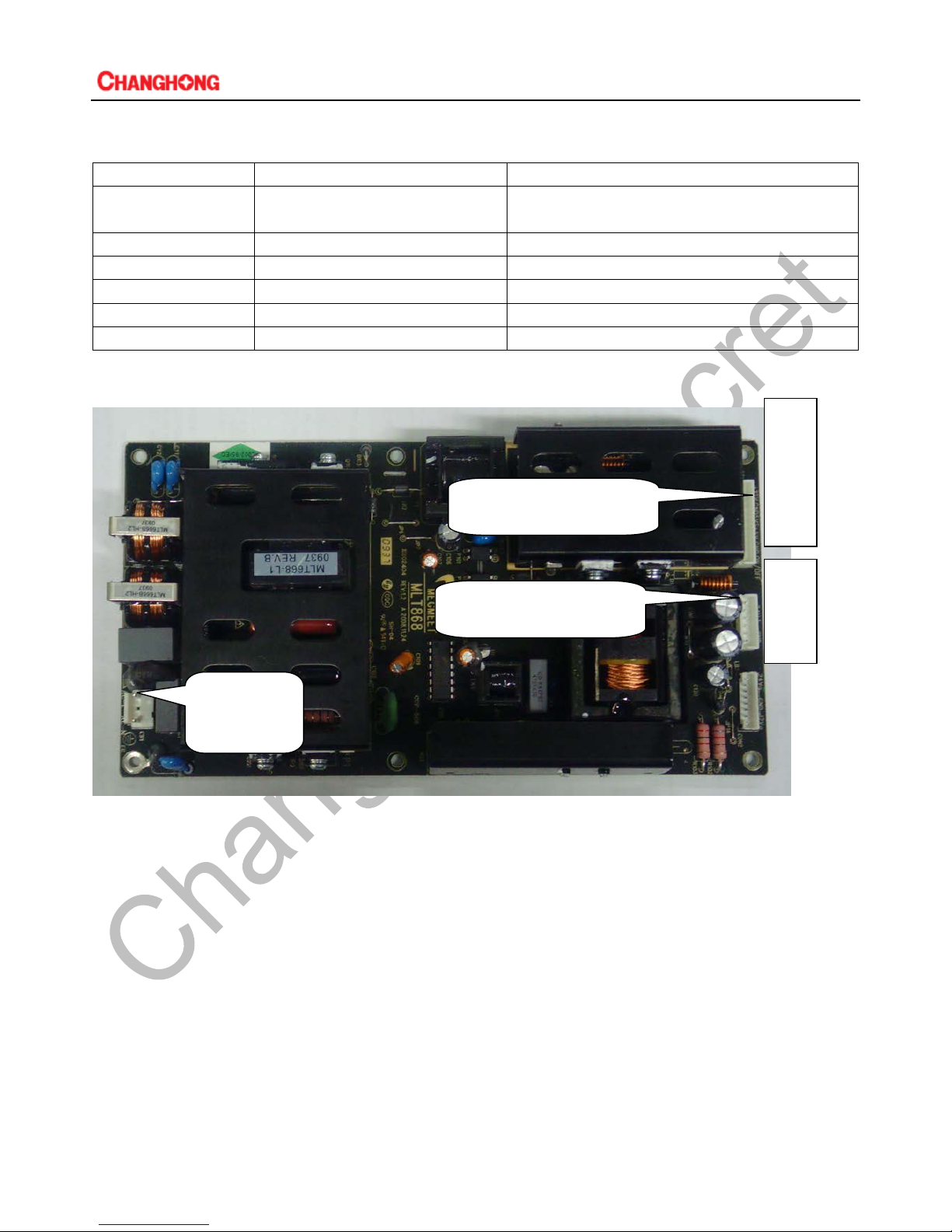
3.3 Brief introduction of power supply
AC input
AC100-240V
50/60HZ
U
se for LCD backlight
power supply.
12V
12V
GND
GND
5VSB
5V
24V
24V
24V
GND
U
se for mainbord power
supply.

9
Chapter4 The chassis frame diagram, mainboard power supply systems,
mainboard interface definition and the waveform of key points
This chapter mainl y introduce the chassis frame diagram , power supply system, interface definition and
each key point’s wave shape.
4-1 The chassis frame diagr am
4-2 Power supply system
Power board has two kinds of output voltage: +12V and +5V.
4-2-1 The composition and distribution of the TV power supply
10
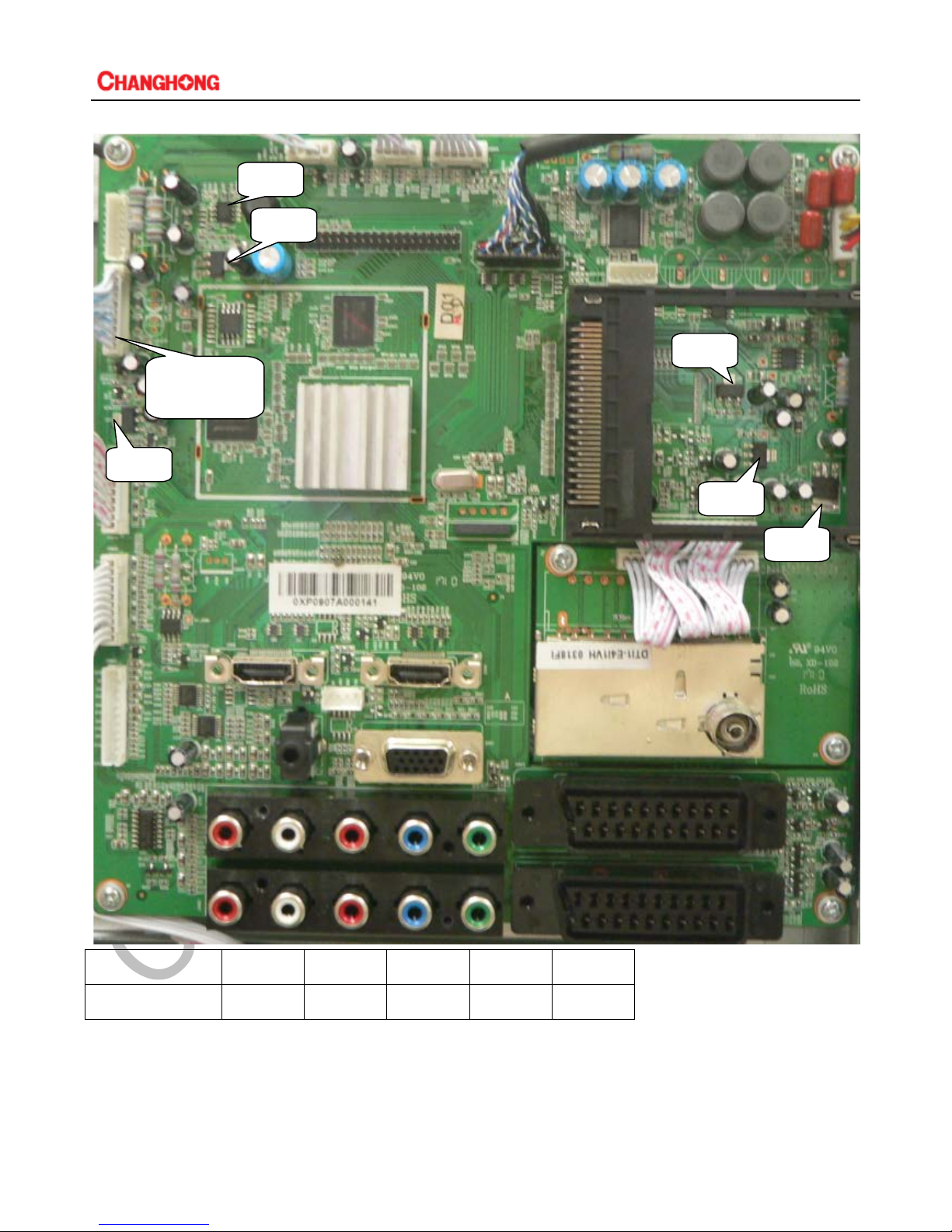
4-2-2 Pin voltage of the voltage adjustor on the mainboard
item No. U39 U51 U37,U38 U36 U18
output voltage 1.8V 1.32V 3.3V 2.5V 5V
3.3V
2.5V
5V
PIN4,5 =5V
PIN9,10=12V
1.8V
1.32V
3.3V
 Loading...