

Page 1

FILE NO. SM-CTV-O-123
SERVICE MANUAL
CHASSIS NO. CH-20
:
Please read this manual carefully before service.
Page 2

TABLE OF CONTENTS
SAFETY INSTRUCTIONS......................................................................................1
ADJUSTMENTS..................................................................................................... 4
STRUCTURE AND CHASSIS FUNCTION DESCRIPTION................................... 17
SERVICE DATA ................................................................................................... 17
REPLACEMENT OF PARTS.................................................................................. 55
APPENDIX CIRCUIT DIAGRAMS
Page 3

SERVICE MANUAL
INSTRUCTIONS FOR SERVICE SAFETY AND MAINTENANCE
ADJUSTMENTS
WARNING: BEFORE SERVICING THIS CHASSIS, READ THE “X-RAY
RADIATION PRECAUTION”, “SAFETY PRECAUTION”AND “PRODUCT
SAFETY NOTICE”INSTRUCTION BELOW.
X-RAY RADIATION PRECAUTION
The EHT must be checked every time the TV is serviced to ensure that the CRT does not emit
1.
X-ray radiation as result of excessive EHT voltage. The maximum EHT voltage permissible in
any operating circumstances must not exceed the rated value. When checking the EHT, use
the High Voltage Check procedure in this manual using an accurate EHT voltmeter.
2. The only source of X-RAY radiation in this TV is the CRT. The TV minimizes X-RAY radiation,
which ensures safety during normal operation. To prevent X-ray radiation, the replacement
CRT must be
3. Some components used in this TV have safety related characteristics preventing the CRT from
emitting X-ray radiation. For continued safety, replacement component should be made after
referring the PRODUCT SAFETY NOTICE below.
4. Service and adjustment of the TV may result in changes in the nominal EHT voltage of the
CRT anode. So ensure that the maximum EHT voltage does not exceed the rated value after
service and adjustment.
identical to the original fitted as specified in the parts list.
SAFETY PRECAUTION
WARNING: REFER SERVICING TO QUALIFIED SERVICE PERSONNEL ONLY.
1. The TV has a nominal working EHT voltage. Extreme caution should be exercised when
working on the TV with the back removed.
1.1 Do not attempt to service this TV if you are not conversant with the preca utions and procedures
for working on high voltage equipment.
1.2 When handling or working on the CRT, always discharge the anode to the TV chassis before
removing the anode cap in case of electric shock.
1.3 The CRT, if broken, will violently expel glass fragments. Use shatterproof goggles and take
extreme care while handling.
1.4 Do not hold the CRT by the neck as this is a very dangerous practice.
2. It is essential that to maintain the safety of the customer all power cord forms be replaced
exactly as supplied from factory.
3. Voltage exists between the hot and cold ground when the TV is in operation. Install a suitable
isolating transformer of beyond rated overall power when servicing or connecting any test
equipment for the sake of safety.
4. When replacing ICs, use specific tools or a static-proof electric iron with small power (below
35W).
5. Do not use a magnetized screwdriver when tightening or loosing the deflection yoke assembly
to avoid electronic gun magnetized and decrement in convergence of the CRT.
1
Page 4

SERVICE MANUAL
6. When remounting the TV chassis, ensure that all guard devices, such as nonmetal control
buttons, switch, insulating sleeve, shielding cover, isolating resistors and capacitors, are
installed on the original place.
7. Replace blown fuses within the TV with the fuse specified in the parts list.
8. When replacing wires or components to terminals or tags, wind the leads around the terminal
before soldering. When replacing safety components identified by the international hazard
symbols on the circuit diagram and parts list, it must be the company-approved type and must
be mounted as the original.
9. Keep wires away from high temperature components.
PRODUCT SAFETY NOTICE
CAUTION: FOR YOUR PROTECTION, THE FOLLOWING PRODUCT SAFETY NOTICE
SHOULD BE READ CAREFULLY BEFORE OPERATING AND SERVICING THIS TV SET.
1. Many electrical and mechanical components in this chassis have special safety-related
characteristics. These characteristics are often passed unnoticed by a visual inspection and
the X-ray radiation protection afforded by them cannot necessarily be obtained by using
replacements rated at higher voltages or wattage, etc. Components which have these special
safety characteristics in this manual and its supplements are identified by the international
hazard symbols on the circuit diagram and parts list. Before replacing any of th ese componen ts
read the parts list in this manual carefully. Substitute replacement components which do not
have the same safety characteristics as specified in the parts list may create X-ray radiation.
2. Do not slap or beat the cabinet or CRT, since this may result in fire or explosion.
3. Never allow the TV sharing a plug or socket with other large-power equipment. Doing so may
result in too large load, causing fire.
4. Do not allow anything to rest on or roll over the power cord. Protect the power cord from being
walked on, modified, cut or pinched, particularly at plugs.
5. Do not place any objects, especially heavy objects and lightings, on top of the TV set. Do not
install the TV near any heat sources such as radiators, heat registers, stove, or other
apparatus that produce heat.
6. Service personnel should observe the SAFETY INSTRUCTIONS in this manual during use and
servicing of this TV set. Otherwise, the resulted damage is not protected by the manufacturer.
SAFETY SYMBOL DESCRIPTION
The lightning symbol in the triangle tells you that the voltage inside this product
may be strong enough to cause an electric shock. Extreme caution should be
exercised when working on the TV with the back removed.
This is an international hazard symbol, telling you that the components identified
by the symbol have special safety-related characteristics.
FDA This symbol tells you that the critical components identified by the FDA marking
have special safety-related characteristics.
UL
This symbol tells you that the critical components identified by the UL marking
2
Page 5

SERVICE MANUAL
have special safety-related characteristics.
C UL
VDE
This symbol tells you that the critical components identified by the C-UL marking
have been evaluated to the UL and C-UL standards and have special
safety-related characteristics.
This symbol tells you that the critical components identified by the VDE marking
have special safety-related characteristics.
MAINTENANCE
1. Place the TV set on a sta ble stand or base that is of adequate size and strength to prevent it
from being accidentally tipped over, pushed off, or pulled off. Do not place the set near or
over a radiator or heat register, or where it is exposed to direct sunlight.
2. Do not install the TV set in a place exposed to rain, water, excessive dust, mechanical
vibrations or impacts.
3. Allow enough space (at least 10cm) between the TV and wall or enclosures for proper
ventilation.
4. Slots and openings in the cabinet should never be blocked by clothes or other objects.
5. Please power off the TV set and disconnect it from the wall immediately if any abnormal
condition are met, such as bad smell, belching smoke, sparkling, abnormal sound, no
picture/sound/raster. Hold the plug firmly when disconnecting the power cord.
6. Unplug the TV set from the wall outlet before cleaning or polishing it. Use a dry soft cloth for
cleaning the exterior of the TV set or CRT screen. Do not use liquid cleaners or aerosol
cleaners.
3
Page 6

SERVICE MANUAL
ADJUSTMENTS
SET-UP ADJUSTMENTS
The following adjustments should be made when a complete realignment is required or a new
picture tube is installed.
Perform the adjustments in the following order:
1. Color purity
2. Convergence
3. White balance
Notes:
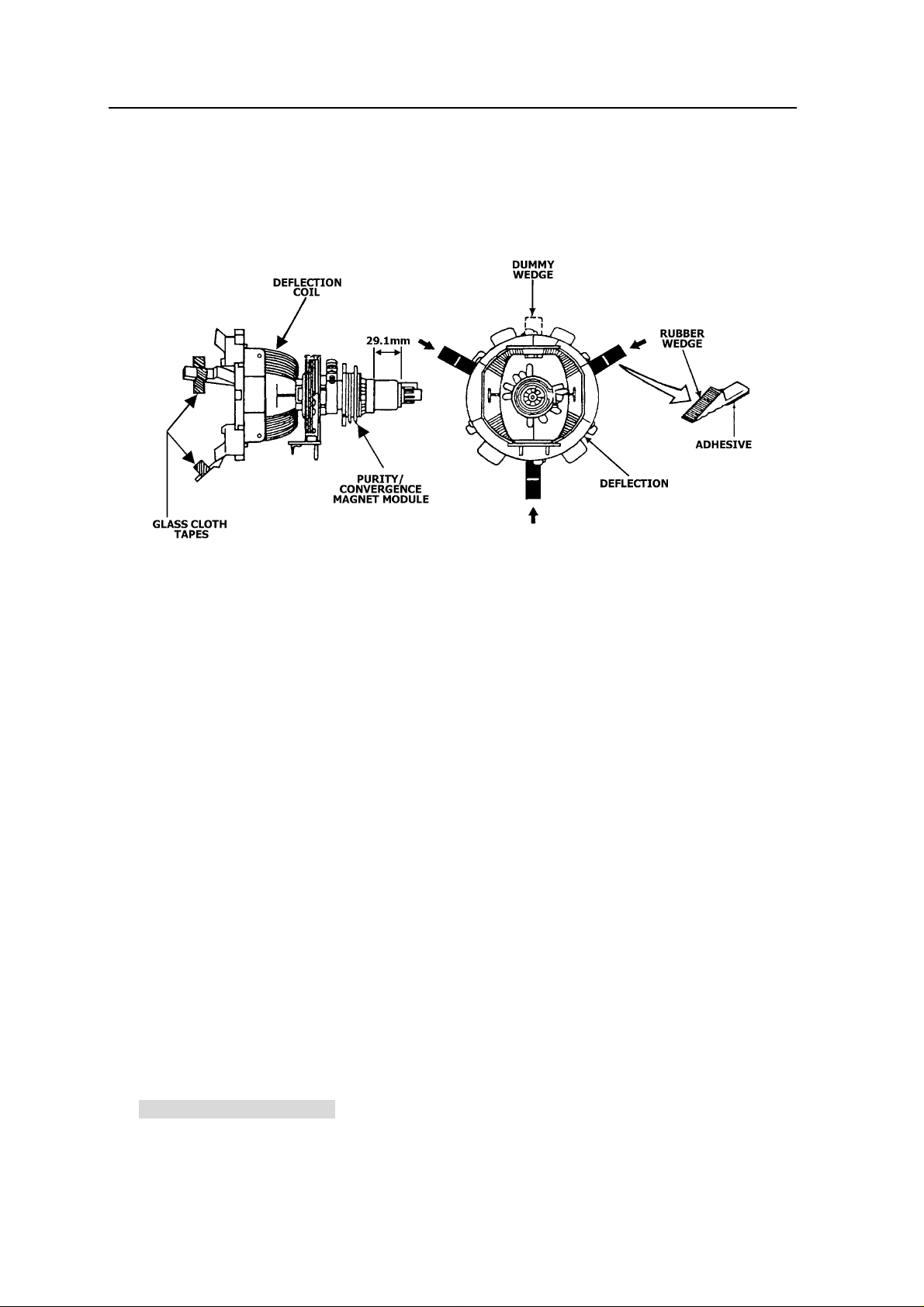
① The purity/convergence magnet assembly and rubber wedges need mechanical
positioning. Refer to Fig1, 2.
② For some picture tubes, purity/ convergence adjustments are not required.
1. Color Purity Adjustment
Preparation:
Before starting this adjustment, adjust the vertical sync, horizontal sync, vertical amplitude and
focus.
1.1 Face the TV set north or south.
1.2 Connect the power plug into the wall outlet and turn on the main power switch of the TV set.
1.3 Operate the TV for at least 15 minutes.
1.4 Degauss the TV set using a specific degaussing coil.
1.5 Set the brightness and contrast to maximum.
1.6 Counter clockwise rotate the R /B low brightness potentiometers to the end and rotate the
green low brightness potentiometer to center.
1.7 Receive green raster pattern signals.
1.8 Loosen the clamp screw holding the deflection yoke assembly and slide it forward or backward
to display a vertical green zone on the screen. Rotate and spread the tabs of the purity magnet
around the neck of the CRT until the green zone is located vertically at t he center of the screen.
1.9 Slowly move the deflection yoke assembly forward or backward until a uniform green screen is
obtained.
1.10 Tighten the clamp screw of the assembly temporarily. Check purity of the red raster and blue
raster until purities of the three rasters meet the requirement.
2. Convergence Adjustment
Preparation:
Before attempting any convergence adjustment, the TV should be operated for at least 15
minutes.
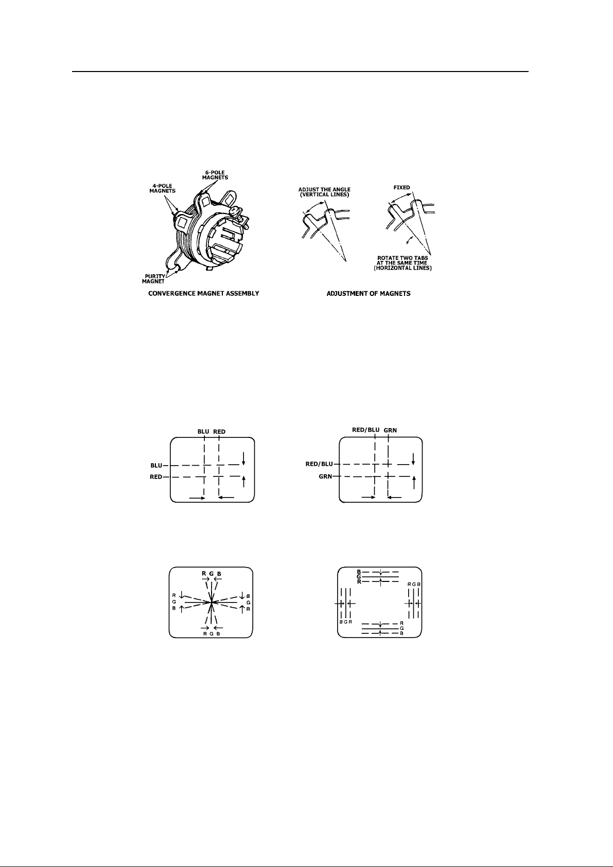
2.1 Center convergence adjustment
2.1.1 Receive dot pattern.
2.1.2 Adjust the brightness/contrast controls to obtain a sharp picture.
4
Page 7
SERVICE MANUAL
2.1.3 Adjust two tabs of the 4-pole magnet to change the angle between them and red and blue
vertical lines are superimposed each other on the center of the screen.
Fig. 1
Yok
2.1.4 Turn both tabs at the same time keeping the angle constant to superimpose red and blue
horizontal on the center of the screen.
2.1.5 Adjust two tabs of the 6-pole magnet to superimpose red/blue line and green line.
2.1.6 Remember red and blue movement. Repeat steps 2.1.3~2.1.5 until optimal convergence is
obtained.
2.2 Circumference convergence adjustment
2.2.1 Loosen the clamp screw holding the deflection yoke assembly and allow it tilting.
2.2.2 Temporarily put the first wedge between the picture tube and deflection yoke assembly.
Move front of the deflection yoke up or down to obtain better convergence in circumference.
Push the mounted wedge in to fix the yoke temporarily.
2.2.3 Put the second wedge into bottom.
2.2.4 Move front of the deflection yoke to the left or right to obtain better convergence in
circumference.
2.2.5 Fix the deflection yoke position and put the third wedge in either upper space. Fasten the
deflection yoke assembly on the picture tube.
2.2.6 Detach the temporarily mounted wedge and put it in either upper space. Fasten the
deflection yoke assembly on the picture tube.
2.2.7 After fastening the three wedges, recheck overall convergence and ensure to get optimal
convergence. Tighten the lamp screw holding the deflection yoke assembly.
3. White Balance Adjustment
Generally, white balance adjustment is made with professional equipment. It’s not practical to
get good white balance only through manual adjustment. For TVs with I
2
C bus control, change
5
Page 8
the bus data to adjust white balance.
SERVICE MANUAL
Fig. 2
4-pole Magnet Movement 6-pole Magnet Movement
Center Convergence by Convergence Magnets
Incline the Yoke Up (or Down) Incline the Yoke Right (or Left)
Circumference Convergence by DEF Yoke
Fig.3
6
Page 9

SERVICE MANUAL
CIRCUIT ADJUSTMENTS
Preparation:
Circuit adjustments should be made only after completion of set-up adjustments.
Circuit adjustments can be performed using the adjustable components inside the TV set. For TVs
2
C bus control, first change the bus data.
with I
1. Degaussing
A degaussing coil is built inside the TV set. Each time the TV is powered on, the degaussing
coil will automatically degauss the TV. If the TV is magnetized by external strong magnetic field,
causing color spot on the screen, use a specific degausser to demagnetize the TV in the
following ways. Otherwise, color distortion will be shown on the screen.
1.1 Power on the TV set and operate it for at least 15 minutes.
1.2 Receive red full-field pattern.
1.3 Power on the specific degausser and face it to the TV screen.
1.4 Turn on the degausser. Slowly move it around the screen and slowly take it away from the TV.
1.5 Repeat the above steps until the TV is degaussed completely.
2. Confirmation and Adjustment for Voltage
Caution: +B voltage has close relation to high voltage. To prevent X-ray radiation, set +B
voltage to the rated value.
2.1 Power on the TV and receive Philips test pattern.
2.2 Check the resistors and coils for being burned. (If the fuse is burned out, do not power on the
TV again until the cause is found out.)
2.3 Measure voltages of test points with the digital voltmeter. Measure the CRT high voltage with
the high-voltage testing equipment and heater voltage with the high-frequency effective
voltmeter. The rated values are shown as table 1
Table 1
Test Point Voltage (V)
One Pin of L807
Positive of C834
Positive of C837
Positive of C832
One Pin of L806
Positive of C839
Positive of VD822
Positive of C429
Positive of C436A
145V±1.5V
12V±1V
12V±1V
16V±1V
16V±1.5V
3.3±0.3V
3.9±0.3V
195V±5V
48V±3V
(Continued)
7
Page 10

SERVICE MANUAL
Positive of C434
Positive of C840
One Pin of 326
Positive of C424
Heater 6.3V±0.3Vrms
CRT anode voltages
3. High Voltage Inspection
Caution: No high voltage adjustment components inside the chassis. Please perform
high voltage inspection in the following ways.
3.1 Connect a precise static high voltmeter to the second anode (inside the high voltage cap) of the
CRT.
3.2 Plug in the supply socket (220V ~, 50Hz) and turn on the TV. Set the brightness and contrast to
minimum (0μA).
3.3 The high voltage reading should be less than the limited EHT voltage.
3.4 Change the brightness from minimum to maximum, and ensure high voltage not beyond the
limitation in any case.
Nominal EHT voltage Limited EHT voltage Remarks
29KV±1.5KV 33KV for 29" CRT
31.0KV±1.5KV 35KV for 34" CRT
Note: The data sheet may differ dependent on different CRTs.
4. Focus Adjustment
Caution: Dangerously high voltages are present inside the TV. Extreme caution should
be exercised when working on the TV with the back removed.
4.1 After removing the back cover, look for the FBT on the main PCB. There should be a FCB on
the FBT.
4.2 Power on the TV and preheat it for 15 min.
4.3 Receive a normal TV signal. Rotate knob of the FCB until you get a sharp picture.
13.5V±1V
8V±0.5V
12V±1V
5V±0.5V
29KV±1.5KV (For 29” CRT)
31.0KV±1.5KV (For 34” CRT)
Before Adjusting After Adjusting
Fig. 4
8
Page 11

SERVICE MANUAL
5. SERVICE mode
5.1 To enter the SERVICE mode
Set the volume to 0 by the remote control. Then press and hold the MUTE button on the
remote control and MENU button on the TV at the same time for over 2 seconds. In the S mode,
press the POWER button to quit the S mode.
Use the ↓/↑buttons on the remote control to highlight an adjustment and the ←/→ buttons
to adjust it.
Bus data
5.2
Item Adjustment Description
S
(“S”is red and other items are yellow.)
Table 2 Bus data
VX00 19 4:3
VX50 01 16:9
VX99 38 ZOOM
5VS/6VS Set to the optimal mode Half vertical center for 50/60Hz
5VA/6VA Set to the optimal mode Vertical amplitude for 50/60Hz
5SC/6SC Set to the optimal mode Vertical S correction for 50/60Hz
5VSH/6VSH Set to the optimal mode Vertical center for 50/60Hz
5VOF/6VOF Set to the optimal mode Character position for 50/60Hz
5HP/6HP Set to the optimal mode Parallelogram correction for 50/60Hz
5HB/6HB Set to the optimal mode Curve correction for 50/60Hz
5HSH/6HSH Set to the optimal mode Horizontal center for 50/60Hz
5HA/6HA Set to the optimal mode Horizontal amplitude for 50/60Hz
5EW/6EW Set to the optimal mode Pincushion and barrel correction for 50/60Hz
5UCR/6UCR Set to the optimal mode Upper corner correction for 50/60Hz
5LCR/6LCR Set to the optimal mode Lower corner correction for 50/60Hz
5TC/6TC Set to the optimal mode Trapezoidal correction for 50/60Hz
RCUT White balance adjustment Red gun cutoff voltage
GCUT White balance adjustment Green gun cutoff voltage
RDRV Dark balance adjustment Red gun drive voltage
GDRV Dark balance adjustment Green gun drive voltage
BDRV 20 Blue gun drive voltage
YDFP 8 PAL brightness delay time
YDFN 2 NTSC brightness delay time
YDFS 2 SECAM brightness delay time
(Continued)
9
Page 12

SERVICE MANUAL
RAGC Set to the optimal mode AGC adjustment(19—1E recommended)
VOL 29 AV output volume control for TDA7442
WBF 30
WBR 30
SOC 1 PWL clip level(5%)
PWL 8 White peak limit
IFO 32 IF phase lock
PEAK 2
BLS 0 Blue extension
BKS 1 Black stretch
CON100 23
CON50 0D
BRI100 32
BRI50 20
COL100 3F Sub color
SHP100 3B
SHP50 1C
VMDL 03 VM delay
VMAM 03 VM amplitude
COR 3
WS 0 White stretch setting
HDOL 0B Cathode drive level
AGCS 1 AGC speed
VG2B 24 Brightness setting when adjusting G2
VENH 03 Vertical enhance
CBNR 03 Comb noise reduce
TRE1 64
TRE2 32
BAS1 64
BAS2 32
VOLA 40/53 MSP3410G/TDA7442
VOLB 46/58 MSP3410G/TDA7442
VOLC 4B/60 MSP3410G/TDA7442
VOLD 51/63 MSP3410G/TDA7442
LOUD 20 Loudness (not for TDA7442)
SC1 74 SCART1 PRESCAL (not for TDA7442)
SC2 74 SCART2 PRESCAL (not for TDA7442)
SCIN 1E SCART IN PRESCAL (not for TDA7442)
FMIN 13 FM frequency bias setting (not for TDA7442)
NNIN 5A NICAM setting (not for TDA7442)
Sub contrast
Sub brightness
Sub sharpness
Treble linearity
Bass linearity
(Continued)
10
Page 13
SERVICE MANUAL
WOCF 1E ( not for TDA7442)
MEFF 44
MAMP FF
MHAR 64
MLOP 19
MHIP 05
OP1
OP2 20 Option set byte 2
OP3 0C Option set byte 3
OP4 11 Option set byte 4
OP5 88 Option set byte 5
OP6 0F Option set byte 6
OP7 08 Option set byte 7
Notes:
① The data sheet may differ dependent on different models.
② The data sheet may differ dependent on different CRTs for the same model.
③ Designs and specifications are subject to change without notice.
Bit Item Description
OP1
OP2
F8 (For PF29T18/34t18 only)
D8 (For CPF29T99 only)
Table 3 Option bit setting
0 OP_NICAM 1: MSP3410;0: TDA7442
1 OP_COMB 1: Yes; 0: No
2 OP_SVM 1: Yes; 0: No
3 OP_AV2 1: Yes; 0: No
4 OP_FAV 1: Yes; 0: No
5 OP_FAVS 1: Yes; 0: No
6 OP_STORE
7 OP_OSO 1
0 OP_AVC
1 OP_MDB
2
3
4
5 OP_ PARENT 1 (Child lock)
Text setting
MDB setting (not for TDA7442)
Option set byte 1
0: West Europe
1: East Europe
1: MSP3410;
0: TDA7442
1: MSP3410;
0: TDA7442
000: West Europe text
001: East Europe text
010: Ukrainian text
100: Russian text
110: Greek text
(Continued)
11
Page 14
SERVICE MANUAL
OP3
OP4
6 OP_TILT Tilt correction
7 OP_FSL 0
1: Black screen available when changing
0 OP_BSCREEN
1 OP_5060 0
2 OP_DK 1: D/K option
3 OP_BG 1: B/G option
4 OP_I 1: I option
5 OP_L 1: L option
6 OP_AUTO_SOUND 1: MSP3410;0: TDA7442
7 OP_EQUAL 1: MSP3410;0: TDA7442
0 OP_FMWS 1
1 OP_POWER
2 OP_COUNTRY 1: COUNTRY display option
3 OP_LOGO 0: LOGO display not available
4 OP_DFL 1
5 OP_BLUE_BACK
6 OP_ACI 1: Yes; 0: No
channels;
0: Black screen not available when changing
channels
1: Memory on
0: Soft on
0: Blue back not available under no signal
condition;
1: Blue back available under no signal
condition
OP5
OP6
7 OP_ATS 1: Yes; 0: No
0 OP_LANG0 0
1 OP_LANG1 0
2 OP_LANG2 0
3 OP_LANG3 0
4 OP_SOUND0 0
5 OP_SOUND1 0
6 OP_SOUND2 1
7 OP_STRIKE 1
0 OP_MUTE 1
1 OP_TUNER 1: West Europe 0: BG
2 OP_AFT 1
3 OP_ENGLISH 1
4 OP_FRANCE 1
5 OP_GERMAN 1
6 OP_SPAIN 1
7 OP_DANMARK 1
(Continued)
12
Page 15

SERVICE MANUAL
0 OP_HOLAND 1
1 OP_SUOMI 1
2 OP_GREECE 1
OP7
3 OP_ITALY 1
4 OP_NORWAY 1
5 OP_PORTUAL 1
6 OP_SWEDEN 1
7 OP_TURKY 1
Note :
① Bit6, Bit5, Bit4 in OP5 are outgoing audio option settings as follows: 000: East Europe
(D/K); 001: West Europe (B/G); 010: UK (I); 110: France (L); 100: Europe (Auto).
② Bit3, Bit2, Bit1 and Bit0 in OP5 are outgoing language option settings as follows:
English, French, German, Spanish, Danish, Dutch, Finnish, Greek, Italian, Norwegian,
Portuguese, Swedish and Turkish successively begun with.
13
Page 16
SERVICE MANUAL
STRUCTURE AND CHASSIS FUNCTION DESCRIPTION
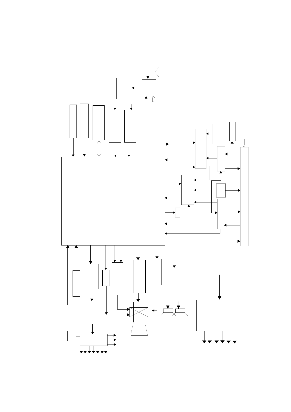
1. Structure Block Diagram
V002
amplifier
IF Pre-
Circuit for Buttons
Remote Sensor
Fig.5 Structure Block Diagram for CH-20 Chassis
AT24C16 (N102)
EEPROM
IIC
K9656M (Z002)
SAW Filter
SIF
K3953M (Z003)
(UOC)
TDA9594 (N101)
Microcontroller
Small Signal Processor &
H-out
V-out-
V-out+
TDA8359 (N401)
EHT Circuit
V402,T401
Including
Line Drive
Vertical Output
E-W
Output V404
ABL Circuit
Horizontal
FBT
+200V
+14V
Voltage
HV
FV
SV
Filament
T402
+8V
+12V-2
+5V
+45V
SAW Filter
VIF
TDA6108JF
A001
Tuner
AGC
R/G/B
Video Amplifier
To VM Coil
CRT
IIC
47
SVM Circuit
73,78
67,68
CTRL SIG
42
38
40
48
SVM
(N501)
TC90A49
CTRL SIG
AV-CVBS
IFO
TV-CVBS
TDA8944J (N603)
Amplifier
Sound Power
Speakers
Comb Filter
Y/C
Trap
R/L
(N301)
Main
Y/C
HEF4052
Video Switch
R/G/B Input
HEF4052 (N302)
Video Switch
CVBS 2
AV-CVBS
CVBS 1 In
Audio Out
+3.3V
Y/C
+3.9V
S- Video In
SCART Jack 2
V1 Out
AV In
Side
SCART Jack 1
V2 Out
50/60Hz
220-240V AC
(N801)
STR-W6856
Power Circuit
+15V-2
+12V
Audio Out
R/L2 Out
R/L2 In
R/L3 In
R/L1 In
R/L1 Out
+145V
+15V-1
IIC
Audio Processor TDA7442 (N602)
14
Page 17
SERVICE MANUAL
2. Block Diagram for Supply Voltage System
Fig.6 Block Diagram for Supply Voltage System for CH-20 Chassis
Circuit N801
Feedback
VD816
+3.9V
VD816
TDA9594 (N101)
TDA9594 (N101)
UOC
UOC
Bus Data
Driver Circuit
LED
Circuit
Hs0038
Remote Sensor
Buttons
Circuit for
VD820
V806
Regulator
+3.3V
AT24C16 (N102)
EEPROM
VD817
+12V-1
Fl501 HFD2-CL2-M
(N801)
STR-W6856
and Control
Power Regulation
Switch Transformer BCK-24339L
VD818
VD815
+15V-1
(N603)
TDA8944J
Amplifier
Circuit
Line Drive
V405
Regulator
TC90A49
Comb Filter
+5V
A001
Tuner
HEF4052
Video Switch
Circuit Including KAV, etc.
Control Signal Driver
+15V-2
Sound Power
lifier V301,V302
V505-V510
Circuit
V303,V304,V310,V311
Video Out Amp-
Y/C Amplifier
ABL & EHT
Audio Out Amplifier
C804,C807,C808
VD801-VD804,C803,
Bridge Rectifier
VD819
+145V
HV
FBT T402
VD410
+12V-2
V808
+8V
TDA9594 (N101)
UOC
TDA7442 (N602)
Audio Processor
V002
IF Amplifier
CRT RGB Board
AC
50/60Hz
220-240V
Circuit
Interference-proof
Filament
SV
FV
Voltage
VD414
VD412
+45V
+200V
TDA6108JF
Video Amplifier
VD003
Regulator
+33V
A001
Tuner
Circuit
Degaussing
VD411
+14V
TDA8359 (N401)
Vertical Output
15
Page 18
SERVICE MANUAL
3. Chassis Description
General Description
CH-20 chassis is applied in CPF29T99/PF29T18/34T18, which mainly uses Philips’ advanced
2
UOC-ultimate one chip TDA959X and I
microcontroller and small signal processor, the TDA959X features high-integrity,
high-performance-to-price ratio and high-reliability and advanced functions with fewer external
components, which provide much more convenience for manufacturing and technical service.
In addition, TDA959X is good in geometric distortion, more suitable for pure flat TV sets.
The following features are available in the chassis:
RF color systems: PAL/SECAM
Video systems: PAL/SECAM/NTSC
Sound systems: D/K B/G I H L L1
100 programs preset
2
C bus control
I
Audio output: Main channel: 7W+7W (distortionless) (THD 7%)
Selectable sound modes: Music, Theatre, Speech, Personal
Selectable picture modes: Personal, Rich, Natural, Soft
AV stereo + audio processing (MSP34XX or TDA7442)
PAL/NTSC 3-line comb filter
Earphone output
Selectable aspect ratio: 4:3, 16:9, Zoom
Auto identification and changeover of vertical frequency 50/60Hz
Auto identification of SCART picture input format (4:3,16:9)
Auto identification of SCART1 signal source input (RGB/CVBS)
The chassis mainly uses the following ICs and assemblies.
Table 4 Key ICs and Assemblies
C-bus controlled IC. With combination of
Serial No. Position Type Function Description
1 N101 TDA9594H Microcontroller and small signal processor (UOC)
2 N102 AT24C16 EEPROM
3 N602 TDA7442 Audio processor
4 N603 TDA8944J Sound power amplifier
5 NY01 TDA6107JF /TDA6108JF Video amplifier
6 N501 TC90A49P COMB Filter
7 N301/N302 HEF4052BP Electronic switch circuit
8 N401 TDA8359J Vertical scan output stage circuit
9 N801 STR-W6856 Power module
10 A001 TDQ-6B3-P/ TAF5-EPB2 Tuner
16
Page 19

SERVICE MANUAL
SERVICE DATA
1. Technical Data of Key ICs
1.1 Microcontroller and Small Signal Processor TDA959X
(1) General Description
The various versions of the TDA959X H/PS-N1 series combine the functions of a video
processor together with a m-Controller and US Closed Caption decoder. Most versions have
a Teletext decoder on board. The Teletext decoder has an internal RAM memory for 1 or 10
page text. Some versions can generate a ‘Mixed-down’ I-signal for the demodulation of DVB
signals. The ICs are intended to be used in economy television receivers with 110 picture
tubes.
The ICs have supply voltages of 8 V and 3.3 V and they are mounted in an SDIP-64 or QFP
80 envelope.
The features are given in the following feature list. The differences between the various ICs
are given in the table.
(2) Features
TV-signal processor
Available in all versions
● Multi-standard vision IF circuit with alignment-free PLL demodulator
● Internal (switchable) time-constant for the IF-AGC circuit
● Integrated chrominance trap circuit Integrated luminance delay line with adjustable delay
time
● Picture improvement features with peaking (with switchable centre frequency, depeaking,
variable positive/negative overshoot ratio and video dependent coring), dynamic skin tone
control and blue- and black stretching
● Scan Velocity Modulation output
● Integrated chroma band-pass filter with switchable centre frequency
● Only one reference (12 MHz) crystal required for the m-Controller, Teletext- and the colour
decoder
● Multi-standard colour decoder with automatic search system
● Internal base-band delay line
● Indication of the Signal-to-Noise ratio of the incoming CVBS signal
● A linear RGB/YUV/YPBPR input with fast blanking for external RGB/YUV sources. The
synchronization circuit can be connected to the incoming Y signal. The Text/OSD signal s are
internally supplied from the m-Controller/Teletext decoder.
● RGB Cathode Calibration’, white point and black level off-set adjustment so that the colour
temperature of the dark and the light parts of the screen can be chosen independently.
● Contrast reduction possibility during mixed-mode of OSD and Text signals
● Adjustable ‘wide blanking’ of the RGB outputs
● Horizontal synchronization with two control loops and alignment-free horizontal oscillator
17
Page 20

SERVICE MANUAL
● Vertical count-down circuit
● Vertical driver optimized for DC-coupled vertical output stages
● Horizontal and vertical geometry processing
● Horizontal and vertical zoom function for 16 : 9 applications
● Horizontal parallelogram and bow correction for large screen picture tubes
● Low-power start-up of the horizontal drive circuit
Available in S-DIP 64 versions
● Sou r c e s e l e ct i o n between t h e ‘ i n t e r n a l ’ C VBS and an external CVBS or Y/C signal
Available in QFP-80 versions
● The mono in tercarrier soun d circuit has a selective F M-PLL demo dulator wh ich can be switched to
the different FM sound freq uencies (4.5/5.5/6 .0/6.5 MHz). The quality of this system is such that the
external band-pass filters can be omitted.
● The FM-PLL demodulator can be set to centre frequencies of 4.74/5.74 MHz so that a second sound
channel can be demodulated. In such an application it is necessary that an external bandpass filter is
inserted.
The vision IF and mono intercarrier sound circuit can be used for the demodulation of FM radio signals
● The QSS and mono FM functionality are both available so that an FM/AM TV receiver can be built
without the use of additional ICs
● Video switch with 2 external CVBS inputs and a CVBS output. One of the CVBS inputs can be used
as Y/C input.
● 2 external audio inputs. The selection of the various inputs is coupled to the selection of the CVBS
signals
● Switchable group delay correction in the CVBS path
● White stretching and a switchable DC transfer ratio for the luminance signal
m-Controller
● 80C51 m-controller core standard instruction set and timing
● 1 ms machine cycle
● 32 - 128Kx8-bit late programmed ROM
● 3 - 12Kx8-bit Auxiliary RAM (shared with Display)
● Interrupt controller for individual enable/disable with two level priority
● Two 16-bit Timer/Counter registers
● One 16-bit Timer with 8-bit Pre-scaler
● WatchDog timer
● Auxiliary RAM page pointer
● 16-bit Data pointer
● Stand-by, Idle and Power Down modes
● 14 bits PWM for Voltage Synthesis Tuning
● 8-bit A/D converter with 4 multiplexed inputs
● 5 PWM (6-bits) outputs for control of TV analogue signals
18
Page 21

SERVICE MANUAL
Data Capture
● Text memory for 1 or 10 pages
● In the 10 page versions inventory of transmitted Teletext pages stored in the Transmitted Page Table
(TPT) and Subtitle Page Table (SPT)
● Data Capture for US Closed Caption
● Data Capture for 525/625 line WST, VPS (PDC system A) and Wide Screen Signalling (WSS) bit
decoding
● Automatic selection between 525 WST/625 WST
● Real-time capture and decoding for WST Teletext in Hardware, to enable optimized m-processor
● Automatic selection between 625 WST/VPS on line 16 of VBI
● throughput
● Automatic detection of FASTEXT transmission
● Real-time packet 26 engine in Hardware for processing accented, G2 and G3 characters
● Signal qua li t y detector for video and WST/VPS data types
● Comprehensive teletext language coverage
● Full Field and Vertical Blanking Interval (VBI) data
● capture of WST data
Display
● Teletext and Enhanced OSD modes
● Features of level 1.5 WST and US Close Caption
● Serial and Parallel Display Attributes
● Single/Double/Quadruple Width and Height for characters
● Scrolling of display region
● Variable flash rate controlled by software
● Enhanced display features including overlining, underlining and italics
● Soft colours using CLUT with 4096 colour palette
● Globally selectable scan lines per row (9/10/13/16) and character matrix [12x10, 12x13, 12x16
(VxH)]
● Fringing (Shadow) selectable from N-S-E-W direction
● Fringe colour selectable
● Meshing of defined area
● Contrast reduction of defined area
● Cursor
● Special Graphics Characters with two planes, allowing four colours per character
● 32 software redefinable On-Screen display characters
● 4 WST Character sets (G0/G2) in single device (e.g. Latin, Cyrillic, Greek, Arabic)
● G1 Mosaic graphics, Limited G3 Line drawing characters
● WST Character sets and Closed Caption Character set in single device
19
Page 22

SERVICE MANUAL
e
(3) Functional Difference between the Various IC Versions
Table 5
IC Version (TDA)
9590PS 9591PS 9592PS
9593PS 9594PS
9590H 9591H 9592H 9593H 9594H
TV range 110 110 110 110 110 110 110 110 110 110
Mono intercarrier multi-standard
sound demodulator (4.5 - 6.5 MHz)
√ √ √ √ √
with switchable centre frequency
Audio switch √ √ √ √ √
Automatic Volume Leveling or
subcarrier output (for comb filter
√ √ √ √ √
applications)
QSS sound IF amplifier with separate
input and AGC circuit
AM sound demodulator without extra
reference circuit
Generation of a ‘Mixed-down’ I-signal
for the demodulation of DVB signals
√ √ √ √ √ √ √ √ √ √
√ √ √ √ √ √ √ √ √ √
√ √ √ √
FM radio option (via QSS amplifier) √ √ √ √ √
FM radio option (with FM tuner) √ √ √ √ √
PAL decoder √ √ √ √ √ √ √ √ √ √
SECAM decoder √ √ √ √ √ √ √ √ √ √
NTSC decoder √ √ √ √ √ √ √ √ √ √
Horizontal geometry (E-W) √ √ √ √ √ √ √ √ √ √
Horizontal and vertical zoom √ √ √ √ √ √ √ √ √ √
ROM size 64 k 64-28k 64 k 32-64k 64-128k 64 k 64-28k 64 k 32-64k 64-128k
User RAM size 2 k 2 k 2 k 2 k 2 k 2 k 2 k 2 k 2 k 2 k
Teletext 10 pag
1 page 10 page 10 page 1 page 10 page
Closed captioning √ √ √ √ √ √ √ √ √ √
20
Page 23

SERVICE MANUAL
A
r
(4) Pinning (QFP-80 ENVELOPE)
26
27
32
33
Pin
Description
port 0.6 (8 mA current sinking capability for direct drive of LEDs) or
Composite video input. A positive-going 1V(peak-to-peak) input is
required
narrow band PLL filter
utomatic Volume Levelling / subcarrier reference output / sound IF
32
input /
external reference signal input for I signal mixer for DVB operation
decoupling sound demodulator
-
QSS intercarrier output / AM output in stereo applications o
35
deemphasis
(front-end audio out) / AM output in mono applications
Symbol
QFP-80 SDIP-64
P3.1/ADC1 1 6 port 3.1 or ADC1 input
P3.2/ADC2 2 7 port 3.2 or ADC2 input
P3.3/ADC3 3 8 port 3.3 or ADC3 input
VSSC/P 4 9 digital ground for m-Controller core and periphery
P0.5 5 10 port 0.5 (8 mA current sinking capability for direct drive of LEDs)
P0.6/CVBSTD 6 11
VSSA 7 12 digital ground of TV-processor
SECPLL 8 13 SECAM PLL decoupling
VP2 9 14 2nd supply voltage TV-processor (+8V)
DECDIG 10 15 supply voltage decoupling of digital circuit of TV-processor
PH2LF 11 16 phase-2 filter
PH1LF 12 17 phase-1 filter
GND3 13 18 ground 3 for TV-processor
DECBG 14 19 bandgap decoupling
EWD 15 20 East-West drive output
VDRB 16 21 vertical drive B output
VDRA 17 22 vertical drive A output
IFIN1 18 23 IF input 1
IFIN2 19 24 IF input 2
IREF 20 25 reference current input
VSC 21 26 vertical sawtooth capacitor
AGCOUT 22 27 tuner AGC output
SIFIN1/DVBIN1 (1) 23 28 SIF input 1 / DVB input 1
SIFIN2/DVBIN2 (1) 24 29 SIF input 2 / DVB input 2
GND2 25 30 ground 2 for TV processor
SNDPLL
AVL/REF0/SNDIF/
REFIN (1)
AUDIO2 28 - audio 2 input
AUDIO3 29 - audio 3 input
HOUT 30 33 horizontal output
FBISO 31 34 flyback input/sandcastle output
DECSDEM
QSSO/AMOUT/
AUDEEM (1)
EHTO 34 36 EHT/over voltage protection input
PLLIF 35 37 IF-PLL loop filter
SIFAGC/DVBAGC (1) 36 31 AGC sound IF / internal-external AGC for DVB applications
INTCO/DVBO (1) 37 - intercarrier output (from QSS or vision IF amplifier) / DVB output
IFVO/SVO/DVBO (1) 38 38 IF video output / selected CVBS output / DVB output
VP1 39 39 main supply voltage TV processor
CVBS1 40 40 internal CVBS input
GND 41 41 ground for TV processor
21
Page 24

SERVICE MANUAL
f
Pin
Symbol
Description
QFP-80 SDIP-64
CVBS2 42 - external CVBS2 input
GND 43 - ground for TV-processor
CVBS3/Y 44 42 CVBS3/Y input
C 45 43 chroma input
WHSTR 46 - white stretch capacitor
CVBSO 47 - CVBS output
AUDOUT /AMOUT 48 - audio output /AM audio output (volume controlled)
SVM 49 44 scan velocity modulation output
INSSW2 50 45 2nd RGB / YUV insertion input
R2/VIN 51 46 2nd R input / V (R-Y) input / PR input
G2/YIN 52 47 2nd G input / Y input
B2/UIN 53 48 2nd B input / U (B-Y) input / PB input
BCLIN 54 49 beam current limiter input
BLKIN 55 50 black current input / V-guard input
RO 56 51 Red output
GO 57 52 Green output
BO 58 53 Blue output
VDDA 59 54
analog supply of Teletext decoder and digital supply o
TV-processor (3.3 V)
VPE 60 55 OTP Programming Voltage
VDDC 61 56 digital supply to core (3.3 V)
OSCGND 62 57 oscillator ground supply
XTALIN 63 58 crystal oscillator input
XTALOUT 64 59 crystal oscillator output
RESET 65 60 reset
VDDP 66 61 digital supply to periphery (+3.3 V)
P1.0/INT1 67 62 port 1.0 or external interrupt 1 input
P1.1/T0 68 63 port 1.1 or Counter/Timer 0 input
P1.2/INT0 69 64 port 1.2 or external interrupt 0 input
P1.3/T1 70 1 port 1.3 or Counter/Timer 1 input
P1.6/SCL 71 2 port 1.6 or I2C-bus clock line
P1.7/SDA 72 3 port 1.7 or I2C-bus data line
P2.0/TPWM 73 4 port 2.0 or Tuning PWM output
P2.1/PWM0 74 - port 2.1
P2.2/PWM1 75 - port 2.2
P2.3/PWM2 76 - port 2.3
P2.4/PWM3 77 - port 2.4
P2.5/PWM4 78 - port 2.5
SYNC_FILTER 79 -
CVBS (i.e. P0.6/CVBS) Sync filter input: This pin should be
connected to VSSA via a 100 nF capacitor.
P3.0/ADC0 80 5 port 3.0 or ADC0 input
Note:
1. The functional content of these pins is dependent on the envelope (SDIP-64 or QFP-80), the mode of
operation and on some I
2
C-bus control bits.
22
Page 25

(5) Black Diagram
)
)
)
(4X)
(
)
SERVICE MANUAL
ROGOBO
BLKIN
BCLIN
+ 3.3 V
PWMS
I/O PORTS (4x
ADC IN (4x
VST OUT
SDA
SCL
LED OUT (2x
1/10 PAGE
MEMORY
TELETEXT/OSD
H
C-BUS
2
I
I/O PORTS
TRANSCEIVER
VST PWM-DAC
TELETEXT
CVBS
BL
B
GB
DISPLAY
RG
V
COR
SYNC
ACQUISITION
CCC
R
WHITE-P. ADJ.
BLUE STRETCH
CONTR/BRIGHTN
OSD/TEXT INSERT
SATURATION
WHITE STRETCH
BLACK STRETCH
RGB/YUV INSERT
Y
U
V
EW GEOMETRY
G/Y B/U BL
R/V
EWD
EHTO
VPE
RESET
AUDOUT
AUDIO3
AUDIO2
ENHANCED
80C51 CPU
ROM/RAM
DELAY LINE
BASE-BAND
V- DRIVE +
GEOMETRY
V
VMOUT
HOUT V-DRIVE
Block diagram
7
Fig .
PEAKING
AVL
AVL
SOUND PLL
DEEMPHASIS
AUDIO SWITCH
VOLUME CO NTROL
VMOUT
LUMA DELAY
DECODER
PAL/SECAM/NTSC
SNDIF
AUDEEM
QSSO/AMOUT
REF
REF
AGC
QSS MIXER
QSS SOUND IF
AM DEMO DU LTOR
SIFIN
TUNERAGC
AGC/AFC
VISION IF
VIDEO AMP.
PLL DEMOD.
DVB MIXER
IFVO/DVBO
VIFIN
TRAP
SOUND
VIDEO IDEN T.
VIDEO SWITCH
GROUP DELAY
CORRECTION
VIDEO FILTERS
CVBS2
CVBSO
CVBS3/Y
C
LOOP
nd
H-SHIFT
H-DRIVE
2
7
H
8
H-OSC. + PLL
H/V SYNC SEP.
+8V
23
Page 26

(6) Pining
SERVICE MANUAL
P3.1/ADC1
P3.2/ADC2
P3.3/ADC3
VSSC/P
P0.6/CVBSTD
SECPLL
DECDIG
PH2LF
PH1LF
DECBG
AGCOUT
DVBIN1/SIFIN1
DVBIN2/SIFIN2
P0.5
VSSA
VP2
GND3
EWD
VDRB
VDRA
IFIN1
IFIN2
IREF
VSC
1
2
3
4
5
6
7
8
9
10
11
12
13
14
15
16
17
18
19
20
21
22
23
24
P2.5/PWM4
P3.0/ADC0
80
SYNC_FILTER
79
P2.3/PWM2
P2.2/PWM1
P2.1/PWM0
P2.4/PWM3
77
75
76
78
TDA959X series
QFP-80
25
GND2
26
27
282930
AUDIO2
SNDPLL
31
HOUT
FBISO
AUDIO3
P1.6/SCL
P1.2/INTO
P1.1/T0
P2.0/PMW
P1.7/SDA
P1.3/T1
71
73
74
72
706968
32
333435
PLLIF
EHTO
DECSDEM
P1.O/INT1
VDDP
RESET
67
65
66
XTALOUT
64
XTALIN
63
OSCGND
62
VDDC
61
VPE
60
VDDA
59
58
BO
57
GO
56
RO
55
BLKIN
54
BCLIN
53
B2/UIN
52
G2/YIN
51
R2/VIN
50
INSSW2
49
SVM
48
AUDOUT /AMOUT
47
CVBSO
46
WHSTR
45
C
44
CVBS3/Y
43
GND
42
CVBS2
41
37
38
36
39
DVBO
SIFAGC/DVBAGC
SVO/IFOUT/DVBO
GND
40
VP1
CVBS1
AVL/REFOUT S N DIF/REFIN
AMOUT/QSSO/AUDEEM
Fig. 8 Pin configuration (QFP-80)
24
Page 27

SERVICE MANUAL
X
P1.3/T1
P1.6/SCL
P1.7/SDA
P2.0/TPMW
P3.0/ADC0
P3.1/ADC1
P3.2/ADC2
P3.3/ADC3
VSSC/P
P0.5
P0.6
VSSA
SECPLL
VP2
DECDIG
PH2LF
PH1LF
GND3
DECBG
EWD
VDRB
VDRA
IFIN1
IFIN2
IREF
VSC
AGCOUT
SIFIN1/DVBIN1
SIFIN2/DVBIN2
GND2
SIFAGC/DVBAGC
REFO/AMOUT/
REFIN
1
2
3
4
5
6
7
8
9
10
11
12
13
14
15
16
17
18
19
20
21
22
23
24
25
26
27
28
29
30
31
32
XX
TDA959X series SDIP-64
64
63
62
61
60
59
58
57
56
55
54
53
52
51
50
49
48
47
46
45
44
SVM
C
43
42
41
40
39
IFVO/SVO/DVBO
38
37
36
QSSO/
35
AMOUT
34
FBISO
33
Fig. 9 Pin configuration (SDIP 64)
(7) Refer to Table 12 about Functions and Data of the IC’s Pins.
P1.2/INT0
P1.1/T0
P1.0/INT1
VDDP
RESET
XTALOUT
XTALIN
OSCGND
VDDC
VPE
VDDA
BO
GO
RO
BLKIN
BCLIN
B2/UIN
G2/YIN
R2/VIN
INSSW2
CVBS/Y
GND
CVBS1
VP1
PLLIF
EHTO
HOUT
25
Page 28

SERVICE MANUAL
/
1.2 EEPROM AT24C16 (N101)
(1) Features
·Low Voltage and Standard Voltage Operation
5.0 (V
2.7 (V
2.5 (V
1.8 (V
= 4.5V to 5.5V)
CC
= 2.7V to 5.5V)
CC
= 2.5V to 5.5V)
CC
= 1.8V to 5.5V)
CC
·Internally Organized 128 x 8 (1K), 256 x 8 (2K),
512 x 8 (4K),1024 x 8 (8K) or 2048 x 8 (16K)
·2-Wire Serial Interface
·Bidirectional Data Transfer Protocol
·100 kHz (1.8V, 2.5V, 2.7V) and 400 kHz (5V)
Compatibility
·Write Protect Pin for Hardware Data Protection
·8-Byte Page (1K, 2K), 16-Byte Page (4K, 8K,
16K) Write Modes
·Partial Page Writes Are Allowed
·Self-Timed Write Cycle (10 ms max)
·High Reliability
Endurance: 1 Million Cycles
Data Retention: 100 Years
·Automotive Grade and Extended Temperature
Devices Available
(3) Pin Configurations
·8-Pin and 14-Pin JEDEC SOIC and 8-Pin
PDIP Packages
(2) Description
The AT24C01A/02/04/08/16 provides
1024/2048/4096/8192/16384 bits of serial
electrically erasable and programmable read
only memory (EEPROM) organized as
128/256/512
The device is optimized for use in many
industrial and commercial applications where
low power and low voltage operation are
essential. The AT24C01A/02/04/08/16 is
available in space saving 8-pin PDIP, 8-pin
and 14-pin SOIC packages and is accessed
via a 2-wire serial interface. In addition, the
entire family is available in 5.0V (4.5V to
5.5V), 2.7V (2.7V to 5.5V), 2.5V (2.5V to
5.5V) and 1.8V (1.8V to 5.5V) versions.
1024/2048 words of 8 bits each.
Fig. 10
26
Page 29

(4) Block Diagram
SERVICE MANUAL
Fig. 11
(5) Refer to Table 13 about Functions and Data of the IC’s Pins.
27
Page 30

SERVICE MANUAL
1.3 Tone Control and Surround Digitally Controlled Audio Processor TDA7442/TDA7442D
(1) Features
4 Stereo Inputs
Input Attenuation Control In 0.5db Step
Treble And Bass Control
Two Surround Mode Available With 4 Selectabler Responses:
- Music
- Simulated Stereo
Two Speaker Attenuators:
- 2 Independent Speaker Controls
In 1db Steps For Balance Facility
- Independent Mute Function
All Functions Programmable Via Serial Bus
2 Monitor Output (Only For Tda7442)
(2) Description
The TDA7442/42D is volume tone (bass and treble) balance (Left/Right) processors for quality audio
applications in TV and Hi-Fi systems. It reproduces surround sound by using a programmable
phase shifter. Control of all the functions is accomplished by serial bus.
The AC signal setting is obtained by resistor networks and switches combined with operational
amplifiers.
Thanks to the BIPOLAR/CMOS Technology used, Low Distortion, Low Noise and DC stepping are
obtained.
(3) Pin Connections
Fig. 11
28
Page 31

(4) Block Diagram (TDA7442)
SERVICE MANUAL
0.47mF
0.47mF
0.47mF
0.47mF
0.47mF
0.47mF
0.47mF
0.47mF
L-IN1
L-IN2
L-IN3
L-IN4
R-IN1
R-IN2
R-IN3
R-IN4
5.6nF
TREBLE-L
OFF
SURR
AMP
AMP
TREBLE BASS
TREBLE BASS
SURR
OFF
Vref
5.6nF
SYMULATED
-
+
100nF
PS1
RPS1
PS1
90Hz
SYMULATED
MUSIC
L-R
OFF
LPF
EFFECT
9KHz
CONTROL
V
LP TREBLE-R
S
1.2nF
MUSIC/
SUPPLY
AGND
MIXING
MIXING
CREF
22mF
2.2mF
MONITOR(L)
MUXOUT(L)
5
50K
6
50K
7
50K
8
50K
2
50K
1
50K
32
50K
31
50K
MONITOR(R)
31.5dB
control
31.5dB
control
4 11 13 182 7 282 6 22 14 13
MUXOUT(R)
IN(L)
30K
-
+
L+R
+
30K
IN(R)
2.2mF
5.6K
100nF
100nF
BOUT(L)
BIN(L)
171620193 109
RB
FIX
I2C BUS DECODER +LATCHES
VAR
RB
BIN(R) BOUT(R)
100nF 100nF
5.6K
79dBCONTROL
MUTE
MUTE
79dBCONTROL
D98AU947B
SPKR
ATT
30
LOUT
24
SCL
25
SDA
23
DIG GND
SPKR
ATT
29
ROUT
-
VAR
+
FIX
FIX
+
-
(5) Block Diagram (TDA7442D)
2.2mF
0.47mF
0.47mF
0.47mF
0.47mF
0.47mF
0.47mF
0.47mF
0.47mF
L-IN1
L-IN2
L-IN3
L-IN4
R-IN1
R-IN2
R-IN3
R-IN4
MUXOUT(L)
4
50K
5
50K
6
50K
7
50K
3
50K
2
50K
1
50K
28
50K
31.5dB
control
31.5dB
control
MUXOUT(R)
IN(L)
30K
-
+
2.2mF
L+R
30K
SYMULATED
IN(R)
+
10 11 16 24 25 23 19 12 13
100nF
PS1
RPS1
PS1
90Hz
MUSIC/
SYMULATED
SUPPLY
AGND
MIXING
MIXING
CREF
22mF
MUSIC
L-R
-
+
OFF
LPF
EFFECT
9KHz
CONTROL
LP TREBLE-R
V
S
1.2nF
5.6nF
TREBLE-L
OFF
SURR
AMP
AMP
TREBLE BASS
TREBLE BASS
SURR
OFF
Vref
5.6nF
5.6K
100nF
100nF
BOUT(L)
BIN(L)
1514181798
RB
FIX
I2C BUS DECODER +LATCHES
VAR
RB
BIN(R) BOUT(R)
100nF 100nF
5.6K
79dBCONTROL
MUTE
MUTE
79dBCONTROL
D01AU1248
SPKR
ATT
SPKR
ATT
27
LOUT
21
SCL
22
SDA
20
DIG GND
26
ROUT
-
VAR
+
FIX
FIX
+
-
29
Page 32

SERVICE MANUAL
a
1.4 Sound Power Amplifier TDA8944J (N603)
(1) General Description
The TDA8944J is a dual-channel audio power amplifier with an output power of
2 × 7 W at an 8Ω load and a 12V supply. The circuit contains two Bridge Tied Load
(BTL) amplifiers with an all-NPN output stage and standby/mute logic. The TDA8944J
comes in a 17-pin DIL-bent-SIL (DBS) power package. The TDA8944J is
printed-circuit board (PCB) compatible with all other types in the TDA894x family.
One PCB footprint accommodates both the mono and the stereo products.
(2) Features
·Few external components
·Fixed gain
·Standby and mute mode
·No on/off switching plops
·Low standby current
·High supply voltage ripple rejection
·Outputs short-circuit protected to ground, supply and across the load
·Thermally protected
·Printed-circuit board compatible.
(3) Block Diagram Pinning
Fig. 10 Block Diagr
m
Fig. 11 Pin Configuration.
(4) Refer to Table 14 about functions and Service Data of the IC’s Pin’s
30
Page 33

SERVICE MANUAL
1.5 Triple Video Output Amplifier TDA6108JF/6107Q
(1) Features
Typical bandwidth of 9.0MHz (for
TDA6108JF) or 5.5MHz (for TDA6107Q)
for an output signal of 60 V (peak-to-peak
value)
·
High slew rate of 1850V/μs (for
TDA6108JF) or 900V/μs (for
TDA6107Q)
·No external components required
·Very simple application
·Single supply voltage of 200 V
·Internal reference voltage of 2.5 V
·Fixed gain of 51 (for TDA6108JF) or 50 (for
TDA6107Q)
·Black-Current Stabilization (BCS) circuit
·Thermal protection.
(2) General Description
The TDA6107Q/6108JF includes three video
output amplifiers in one plastic DIL-bent-SIL
9-pin medium power (DBS9MPF) package (SOT
111-1), using high-voltage DMOS technology,
and is intended to drive the three cathodes of a
colour CRT directly. To obtain maximum
performance, the amplifier should be used with
black-current control.
(3) Ordering Information
Table 6
Type
Number
Name Description Version
Package
Plastic
DIL-bent-SIL
TDA6108JF/
DBS9MPF
medium power
TDA6107Q
package with fin;
SOT111-1
(4) Block Diagram
9 leads
Fig. 12
31
Page 34

Table 7 Pinning
g
SERVICE MANUAL
Symbol Pin Description
V
1 Inverting input 1
i(1)
V
2 Inverting input 2
i(2)
V
3 Inverting input 3
i(3)
GND 4 ground (fin)
Black-current
Iom 5
measurement output
VDD 6 Supply voltage
V
7 Cathode output 3
oc(3)
V
8 Cathode output 2
oc(2)
V
9 Cathode output 1
oc(1)
(5) Refer to Table 15 about Functions and Data of the IC’s Pins.
Fig. 13 Pin Confi
uration.
32
Page 35

SERVICE MANUAL
1.6 COMB Filter TC90A49P (N1)
(1) Features
·TV format : NTSC (3.58), PAL, M-PAL, and N-PAL
·Dynamic comb filter
·Vertical edge enhancement circuit
·PLL 8 × multiplier circuit
·Internal 8-bit 4 fsc AD converter
·Internal 8-bit precision 8 fsc DA converter (2 ch)
·Sync tip clamp circuit
·Internal 4H-line memory
2
·I
C bus interface
·Package : DIP 20-pin and SOP 24-pin
·5V single power supply
(2) Block Diagram
(3) Pin Assignment
Fig. 14
Fig. 15
Fig. 16
(4) Refer to Table 16 about Functions and Service Data of the IC’s Pins.
33
Page 36

SERVICE MANUAL
1.7 Dual 4-channel Analog Multiplexer/Demultiplexer HEF4052
(1) Description
The HEF4052 is a dual 4-channel analog multiplexer/demultiplexer with common channel select
logic. Each multiplexer/demultiplexer has four independent inputs/output s (Y
input/output (Z). The common channel select logic includes two address inputs (A
to Y3) and a common
0
and A1) and an
0
active LOW enable input (E).
Both multiplexers/demultiplexers contain four bidirectional analog switches, each with one side
connected to an independent input/output (Y
to Y3) and the other side connected to a common
0
input/output(Z).
With E LOW, one of the four switches is selected (low impedance ON-state) by A
HIGH, all switches are in the high impedance OFF-state, independent of A
are the supply voltage connections for the digital control inputs (A
is 3 to 15 V. The analog inputs/outputs (Y
and V
V
as a negative limit.
EE
may not exceed 15 V.
DD VEE
to Y3, and Z) can swing between V
0
, A1 and E). The VDD to Vss range
0
0
and A1. With E
0
and A1. VDD and Vss
as a positive limit
DD
For operation as a digital
multiplexer/demultiplexer, V
V
(typically ground)
SS
is connected to
EE
YOA to Y3A Independent inputs/outputs
YOB to Y3B Independent inputs/outputs
Table 8 Pinning
(2) Block Diagrams
AO A1 Address inputs
E Enable input (active LOW)
ZA ZB Common inputs/outputs
Family data, lDD LIMITS category MSI
See Family Specifications
Fig. 17
HEF4052P (N): 16-lead DIL; plastic
(SOT38-1)
HEF4052D (F): 16-lead DIL;
(cerdip) (SOT74)
HEF4052T (D): 16-lead SO;
(SOT109-1)
( ): Package Designator North America
Fig. 18Pinning Diagram
ceramic
plastic
34
Page 37

(3) Function Table
SERVICE MANUAL
Fig. 19 Schematic Diagram (One Switch)
Table 9
Inputs Channel
E A1 A
L L L YOA-ZA; YOB-ZB
L L H Y1A-ZA; Y1B-ZB
L H L Y2A-ZA; Y2B-ZB
L H H Y3A-ZA; Y3B-ZB
H X X none
On
0
Notes
H=HIGH state (the more positive voltage)
L=LOW state (the less positive voltage)
X=state is immaterial
Ratings
Limiting values in accordance with the Absolute Maximum System (IEC 134)
Supply voltage (with reference to V
Note
To avoid drawing V
voltage drop across the bidirectional switch must not exceed 0,4V. If the switch current flows into
terminal Z, no V
across the switch, but the voltages at Y and Z may not exceed V
(4) Refer to Table 17 about Functions and Data of the IC’s Pins.
current out of terminal Z, when switch current flows into terminals Y, the
DD
current will flow out of terminals Y, in this case is no limit for the voltage drop
DD
) VEE -18 to +0,5 V
DD
or V
DD
EE
35
Page 38

SERVICE MANUAL
1.8 Vertical deflection output TDA8359J
(1) Introduction
The TDA8359J is an integrated power circuit for use in 90° and 110° colour deflection systems. It
contains a vertical deflection bridge output, operating as a high efficiency class G system and can
handle field frequencies from 25 to 200 Hz. The vertical coil of a 4 : 3 as well a 16 : 9 picture tube
can be connected to this vertical deflection device. Due to the bridge configuration a DC deflection
output application can be designed with a positive main supply of typical 12 Volts and a positive
flyback supply of typical 45 Volt. (Depending on the coil data).
This integrated circuit is designed in a Low Voltage DMOS (LVDMOS) process that combines
bipolar, CMOS and DMOS components. DMOS output transistors (MOSFETs) are used because of
the absence of secondary breakdown, which gives a better SOAR performance . The internal circuits
are designed in such way that only a few external components are needed to get a correct working
application.
The TDA8359J is functional the same as the TDA8357J vertical deflection output stage. The
TDA8359J differs in only one aspect from the TDA8357J, it is able to deliver a higher output current
which is more suitable for large picture tubes.
A detailed investigation procedure to determine an optimum application is given at the end of this
report.
(2) Features
· Few external components required
· High efficiency fully DC coupled vertical bridge output circuit
· Short rise and fall time of the vertical flyback switch
· Picture tube burn in protection signal (guard circuit)
· Temperature (thermal) protection circuit
· Differential mode inputs
· Blanking pulse generator (guard)
· Improved EMC performance due to differential inputs
(3) Pinning
Table 10
Symbol Pin Description
INA 1 Input A
INB 2 Input B
VP 3 Supply voltage
OUTB 4 Output B
GND 5 Ground
VFB 6 Flyback supply voltage
OUTA 7 Output A
INA
INB
V
OUTB
GND
V
FB
OUTA
GUARD
FEEDB
2
3
P
4
5
TDA835 9J
6
7
8
9
GUARD 8 Guard output
FEEDB 9 Feedback input
Fig. 20
36
Page 39

(3) Block Diagram
V
V
i(bias)
i(p-p)
0
V
i(p-p)
V
i(bias)
0
INA
INB
SERVICE MANUAL
GUARD
863
GUARD
CIRCUIT
1
INPUT
AND
FEED
BACK
CIRCUIT
2
VV
P
M2
D1
M4
M1
M3
FB
M5
D3
D2
OUTA
7
9
FEEDB
4
OUTB
5
TDA8359J
GND
Fig. 21
37
Page 40

SERVICE MANUAL
1.9 Switch-mode Power Supply STR- W68XX
(1) General Description
The STR-W6800 Series are thick-film ICs for Quasi-Resonant flyback SMPS with MOSFET and
control built-in, featuring fewer external components, simplified circuit design, small-size and
standard power supply.
“STR-W6800 Series ICs” offers three operation modes: Quasi-Resonant, Multi-Bottom Skip and
Time Fix Control, thus guaranteeing high efficiency in all loading areas by means of the automatic
change-over of the operation modes.
QR---- Quasi-Resonant operation at the time of heavy load
MBS---- Multi-Bottom Skip operation at the time of medium load for preventing oscillating f requency
rising up and fixing operating frequency
TFC---- Time Fix Control at the time of light load such as stand-by load
By adopting chip-on-chip construction, even small package can deal with big power.
(2) Features
Seven-pin small SIP style package FM207 (generally called TO220), affording dielectric
isolation
Guarantees space of 1.8mm between high voltage pin and other pins, thus high voltage
MOSFET built-in allowed
Offers low startup current by employing BCD-Process
Automatic change-over of QR and MBS operations
With MOSFET turn-on at the bottom of VDS, "STR-W 6800 Series ICs" offers high efficiency
and low noise at the wide areas from the heavy load to stand-by load and fixed operating
frequency, and enables SMPS to become smaller.
TFC operation delivers low-power standby mode for fixing turn-on time, enabling external
components to adjust turn-on time.
Avalanche breakdown energy-guaranteed and high damage-resistance power MOSFET
By guaranteeing avalanche breakdown energy of built-in power MOSFET, "STR-W 6800
Series ICs" simplifies design of absorption circuit of surge voltage without VDSS residual
considered during design.
MOSFET fixed voltage drive circuit built in
Various protection functions
Pulse-by-pulse over-current protection
Over-voltage protection →lockout
Over-load protection →lockout
Thermal protection →lockout (not for STR-W6854/6)
38
Page 41

SERVICE MANUAL
(3) Black Diagram
Vcc
4 Pin
+
RTFC
7 Pin
-
OVP
TSD
REG
+
-
OLP
Current
Mirror
FB/OLP
6 Pin
LATCH
R
S
Current
Mirror
OSC
Q
TFC
BEC
Fig. 22
Drive REG
REG
+
-
BD
BIC
D
1 Pin
DRV
S/GND
3 Pin
OCP/BD
5 Pin
+
OCP
-
(4) Pinning
Table 11
Pin No. Symbol
1 D
2 NC
3 S/GND
4 Vcc
5 OCP/BD
Name
Source for MOSFET
Source/GND for MOSFET
Supply voltage
Over-current protection
Function Description
Source/ GND for Control
detection/Bottom detection
6 FB/OLP
Feedback/Over-load protection
detection
7 RTFC
Time Fix Control regulation
(5) Refer to Table 18 about Functions and Data of the IC’s Pins.
39
Page 42

SERVICE MANUAL
2. WAVEFORMS OF KEY POINTS
Waveform during C802 Startup
Waveform during +B Voltage Startup
40
Page 43

SERVICE MANUAL
41
Page 44

SERVICE MANUAL
42
Page 45

SERVICE MANUAL
43
Page 46

SERVICE MANUAL
44
Page 47

SERVICE MANUAL
Waveform during V404’s Base
T=64us
45
Page 48

SERVICE MANUAL
Waveform during V404’s C Electrode
46
Page 49

SERVICE MANUAL
47
Page 50

3. SERVICE DATA OF KEY ICS
Table 12 Functions and Service Data of TDA9594H (N101)’s Pins
SERVICE MANUAL
Pin No. Function Description
1 P3.1/ADC1 6.8
2 P3.2/ADC2 6.8
3 P3.3/ADC3 1.3 0.196
4 VSSC/P 0 0
5 P0.5 10.4 0
6 P0.6/CVBSTD 10.4 0
7 VSSA 0 0
8 SECPLL 5,420
9 VP2 1.1 7.68
10 DECDIG 30.6
11 PH2LF 5,410
12 PH1LF 5,450
13 GND3 0 0
Resistance to Ground
(KΩ)
Reference Voltage
(V)
14 DECBG 38
15 EWD 1,760
16 VDRB 3.03
17 VDRA 3.03
18 IFIN1 36.4 1.89
19 IFIN2 36.4 1.9
20 IREF 38.9
21 VSC 5,440
22 AGCOUT 1.7 2.0
23 SIFIN1/DVBIN1 (1) 36.5 1.89
24 SIFIN2/DVBIN2 (1) 36.6 1.89
25 GND2 0 0
26 SNDPLL - -
(Continued)
48
Page 51

SERVICE MANUAL
27 AVL/REF0/SNDIF/REFIN (1) 3,680 2.4
28 AUDIO2 - 29 AUDIO3 - 30 HOUT 7,660 3.2
31 FBISO 1,360 0.9
32 DECSDEM 5,290
QSSO/AMOUT/
33
AUDEEM (1)
34 EHTO 7.4 2.54
35 PLLIF 5,440
36 SIFAGC/DVBAGC (1) 5,000
37 INTCO/DVBO (1) - 38 IFVO/SVO/DVBO (1) 3,660 2.05
3,690 0.6
39 VP1 1.1 7.6
40 CVBS1 5,230
41 GND 0 0
42 CVBS2 5,380
43 GND 0 0
44 CVBS3/Y 5,340 3.74
45 C 82.3 1.47
46 WHSTR 5,190
47 CVBSO 5,500
48 AUDOUT /AMOUT 5,500
49 SVM 5,500 4.5
50 INSSW2 0.075
51 R2/VIN 5,500 2.5
52 G2/YIN 5,500 2.5
53 B2/UIN 5,500 2.5
54 BCLIN 0.069 3.7
55 BLKIN 23 3.2
56 RO 5.8 2.7
(Continued)
49
Page 52

SERVICE MANUAL
57 GO 5.8 2.6
58 BO 5.8 2.7
59 VDDA 0.28 3.2
60 VPE 0 0
61 VDDC 0.28 3.3
62 OSCGND 0.014
63 XTALIN 2,500 1.5
64 XTALOUT 5 1.5
65 RESET 0 0
66 VDDP 0.28 3.3
67 P1.0/INT1 10 0.06
68 P1.1/T0 10 0.06
69 P1.2/INT0 12,200 3.3
70 P1.3/T1 0.19 0.7
71 P1.6/SCL 8.7 3.7
72 P1.7/SDA 9 3.8
73 P2.0/TPWM 10.5 0.06
74 P2.1/PWM0 2.5 0.1
75 P2.2/PWM1 3.7 0.06
76 P2.3/PWM2 6.2 0.05
77 P2.4/PWM3 - 78 P2.5/PWM4 10.6 0.1
79 SYNC_FILTER 3,700
80 P3.0/ADC0 - -
50
Page 53
SERVICE MANUAL
Table 13 Functions and Service Data of AT24C16 (N102)’s Pins
Digital Multimeter
Pin
Functions Description
No.
1 Address input 0 0 0
2 Address input 0 0 0
3 Address input 0 0 0
4 Common ground 0 0 0
5 Serial data 4 6.37 6.4
6 Serial clock input 4.2 6.37 6.44
7 Write protect 0 0 0
8 Supply voltage 4.9 3.03 3.02
Reference Voltage
(V)
Positive Resistance
(20KΩ)
Negative Resistance
(20KΩ)
Table 14 Functions and Service Data of TDA8944J (N603)’s Pins
Digital Multimeter
Pin
Functions Description
No.
1 Negative loudspeaker terminal 1 7.98
2 Ground channel 1 0 0 0
3 Supply voltage channel 1 14.9 5.8 7.7
4 Positive loudspeaker terminal 1 7.3
5 Not connected 0
6 Positive input 1 7.3
7 Not connected 0
8 Negative input 1 7.4
9 Negative input 2 7.3
Mode selection input (standby,
10
mute, operating)
Reference Voltage
(V)
0 7.8 8.9
Positive Resistance
(20KΩ)
∞ ∞
∞ ∞
∞ ∞
∞ ∞
∞ ∞
∞ ∞
∞ ∞
Negative Resistance
(20KΩ)
Half supply voltage decoupling
11
(ripple rejection)
12 Positive input 2 7.3
7.6
∞ ∞
∞ ∞
(Continued)
51
Page 54

SERVICE MANUAL
13 Not connected 0
14 Negative loudspeaker terminal 2 7.3
15 Ground channel 2 0 0 0
16 Supply voltage channel 2 14.8 3.5 3.5
17 Positive loudspeaker terminal 2 7.3
∞ ∞
∞ ∞
∞ ∞
Table 15 Functions and Service Data of TDA6107Q/TDA6108JF (NY01)’s Pins
Digital Multimeter
Pin No.
1
2
3
Function Description
G inverting input 3.33 5.32 4.72
R inverting input 3.26 5.32 4.72
B inverting input 3.28 5.32 4.72
Reference Voltage
(V)
Positive Resistance
(20KΩ)
Negative Resistance
(20KΩ)
Ground 0.00 0.00 0.00
4
Black level current input 6.03 18.65 5.65
5
Supply voltage 199
6
B output 69.9
7
R output 69.18
8
G output 65.9
9
Table 16 Functions and Service Data of TC90A49P (N501)’s Pins
Pin
Functions Description
No.
ADC and DAC analog power
1
supply.
ADC bias voltage. Stabilize by
2
attaching a 0.01µF capacitor.
∞
∞
∞
∞
Digital Multimeter
Reference Voltage
(V)
4.98 0.55 0.54
1.41
Positive
Resistance (20KΩ)
∞ ∞
4.48
5.45
5.45
5.45
Negative
Resistance (20KΩ)
(Continued)
52
Page 55

SERVICE MANUAL
ADC input range D upper limit
3
voltage. Stabilize by attaching a
0.01µF capacitor.
ADC input. Inputs 1.0 Vp-p video
4
signal. Sync tip clamp is performed.
ADC input range D lower limit
5
voltage. Stabilize by attaching a
0.01µF capacitor.
6 ADC and DAC logic power supply. 4.98 0.55 0.55
Logic and internal DRAM GND
7
(digital).
8 Internal DRAM power supply 4.98 0.55 0.55
9 I2C BUS SDA 4.12 6.39 6.44
3.15 0.64 0.63
2.14
1.84 0.497 0.49
0 0 0
∞ ∞
10 I2C BUS SCL 4.25 6.4 6.45
2
Shipment test mode switch or I
11
bus setting reset pin.
Y signal comb function ON / OFF
12
switch.
13 Clock input pin. 2.54
Connect the APC filter in the 8 fsc
14
PLL circuit
15 PLL power supply 4.98 0.55 0.55
16 ADC, DAC, and PLL GND (analog). 0 0 0
17 Outputs chrominance signal. 2.25
DAC output range D upper limit
18
voltage.
DAC output range D lower limit
19
voltage
C
0 0 0
0 0 0
∞ ∞
0
3.14 0.57 0.57
1.84 0.42 .043
∞ ∞
∞ ∞
20 Outputs luminance signal. 2.16
∞ ∞
53
Page 56

SERVICE MANUAL
Table 17 Functions and Service Data of HEF4052 (N301/N302)’s Pins
No.
1
2
3
4
5
6
7
8
9
10
11
12
13
Function Description
Signal input 0 12.52 6.46
Signal input 0 12.5 6.46
Signal input 0 12.52 6.46
Signal output 0 12.43 6.25
Signal input 0 12.5 6.46
Ground 0 0 0
Ground 0 0 0
Ground 0 0 0
Control signal input 4.98 7.8 5.6
Control signal input 4.98 7.8 5.6
Control signal input 0 0 0
Signal input 0 0 0
Signal output 0 0 0
Reference Voltage (V)
Digital Multimeter Pin
Positive Resistance (KΩ)
Negative Resistance (KΩ)
14
Signal input 0 0 0
15
Audio output 0 12.48 6.46
16
Supply voltage 5.09 6.89 4.44
Table 18 Functions and Service Data of STR-W6856 (N801)’s Pins
Pin No. Symbol
1
2
3
D
NC
S/GND
Reference Voltage
(V)
303 ∞
0 1.3
16.7 ∞
Resistance to Ground
(MΩ)
4 Vcc 3.1 8.5
5 OCP/BD 1.5 1.3
6 FB/OLP 7.2 1.6
7
RTFC
54
Page 57

SERVICE MANUAL
REPLACEMENT OF PARTS
1. Description
Many electrical and mechanical components in this chassis have special safety-related
characteristics. Components which have these special safety characteristics in this manual
and its supplements are identified by the international hazard symbols or UL, FCC, FDA or
VDE marking on the circuit diagram and parts list. When replacing any of these components,
substitute the one which has the same safety characteristics as specified in the manual.
Description of the special markings:
A: The components identified by the A marking have special safety-related characteristics.
AE: The components identified by the AE marking are listed by EMC and have special
safety-related characteristics.
CB: The components identified by the CB marking have been evaluated to the CB standard.
E: The components identified by the E marking are listed by EMC
G: The components identified by the G marking have critical characteristics.
Z: The components identified by the Z marking have important characteristics.
Note:
Models and specifications of components in this table may be somewhat different with your unit.
In this case, please rely on the actual unit.
55
Page 58

Circuit Diagram for PF29T18 (2)
This circuit diagram is only for reference, specifications are subject to change without reference.
1. Any components identified by have special safety-related characteristics. Use replacement
Which have the same characteristics as original parts.
2. Cold ground Hot ground
Page 59

Circuit Diagram for PF29T18 (1)
This circuit diagram is only for reference, specifications are subject to change without reference.
1. Any components identified by have special safety-related characteristics. Use replacement
Which have the same characteristics as original parts.
2. Cold ground Hot ground
 Loading...