

Page 1

PDP TELEVISION
SERVICE MANUAL
Chassis NO. PS08
Model No. PT4216
Please read this manual carefully before service.
1
Page 2

CONTENTS
PartⅠ:PS08 Chassis Features and Circuit block diagram..………..............................3
PartⅡ:Introduction on main components functions of PT4216 ...……………………7
PartⅢ:Analysis on Signal Process Flow of PT4216 and key point test data ………..24
PartⅣ:Typical troubleshooting process flowchart of PT4216……..............................33
PartⅤ: Spare part list…………………………………………………………………...39
PartⅥ:Factory mode setup and attention…………………………………………40
Annex: 1、Circuit schematic diagram of PT4216……………………………………41
2、Final Assembly diagram of PT4216……....................................................60
3、Final Wire Connection diagram of PT4216………………………………61
2
Page 3

PartⅠ:PS08 Chassis Features and Circuit block diagram
1、 PT4216/PT4218 Panel Datas:
PT4216/ PT4218 and PT5016 are all belong to PS08 chassis. The used panel parameter is below:
PDP Panel Resolution
Colors 16,777,216
Dot Pitch
Brightness High brightness
Contrast High contrast
Lifespan of Panel 20000 Hours
Viewing Angle
Valid display area
Remarks: Brightness and contrast may vary because of different panels being used. PT4216 mainly uses LG
PDP42V7 panel model or Panasonic MD42M7、MD42M8 panel model .注
2、Main Features:
z Radio Frequency input; support CATV
Capable to receive the full CATV programs.
z PIP function
z DVI digital RGB input
z VGA analog RGB input
z High definition YPbPr input
z AV input
Capable to receive NTSC/PAL/SECAM AV signal. Convenient to watch VCR,DVR,DVD programs. Make you into
perfect AV world.
z AV audio and video output
Capable to output one way video, left and right audio signal each one.
z Y/C component video input
S-video input, convenient to connect Y/C video input from DVD output.
z 236 programs preset
In TV condition, capable to save 236 programs. Ready for future rich programs.
z Multi format
Capable to receive NTSC/PAL/SECAM TV signal. Capable to receive D/K,I,B/G,M audio format TV signal.
z On/off on time
Set PDP TV on or off at preset time.
z Blue background mute noise
In TV, AV (S-Video), YCbCr, and YPbPr modes, screen displays gentle blue background if there is no signal input
and into mute condition.
z Auto Off if no signal input
In TV mode, the PDP TV will automatically power off within 15 minutes and enter into standby condition.
z Chinese/English menu
Ordinary and graphical user interface makes the menu operation more convenient and intuitionistic
z Power Energy Saving Mode (power management mode)
In PC mode, the PDD TV will automatically power off within 30 seconds and enter into the Power Energy Saving
Mode if there is no signal input. It will automatically exit from the Power Energy Saving Mode and work again
when it received a valid signal or press any button on the panel/remote control.
z Plug and Play
It is no need to equip any installation software when the product is used as computer terminal display equipment. It
852×3(RGB)×480
1.095mm(H)×1.110mm(V)
U/D:160 / L/R:160
933mm(H)×533mm(V)
3
Page 4
is real plug and play.
z Little weight, small dimension, low power consumption
3、CBU Content
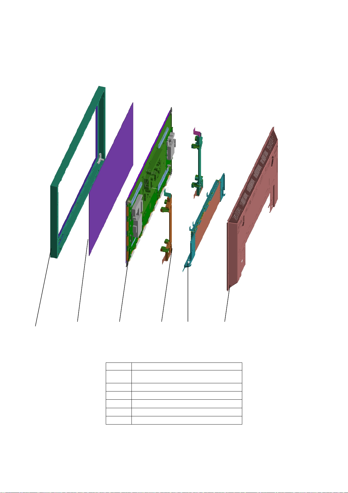
3.1 PDP Inside Drawing:
1 2 3 4 5 6
No. Name
①
②
③
④
⑤
⑥
Front Cabinet
Filter Glass
PDP Panel Module
Shelve Bar
Down Cover Module etc.
Back Cabinet
4
Page 5

Remarks: This drawing is for references only, please see the main assembly diagram and wire-connecting diagram for
details.
3.2
Circuit block diagram:
PS08 chassis PDPD TV is mainly composed of regulator circuit、RF circuit、video processor circuit、Power Amplify
circuit、Analog Video circuit、System Control circuit and Key Control circuit, block diagram of unit circuit is below:
Power Board
+6V
Main Board
IF
+32V
+12V
+5VS
UOCIII
+3.3V
+12VAU
Analog
G
R
CVBS
TDA8759
B
SAA7115
Audio
G
R
24bit
ITU-R656
Panel
Control Signal
B
GM1601
L V D S
k Panel
IR
Panel
FLASH
Speaker
TA2024
audio amplify board
Main
Tuner
SubTuner
HDTV
DVI
PC
AV Board
3.3 PCB assembly introduction
It is mainly composed of AV Board、Remote Control Receiving board 、K Board 、power board、power amplifier
board and Main Board. Herein introduct function of each PCB module:
Number Parts Description
1 Main Board
assembly
2 AV Board
assembly
It is the core of signal processing for PDP TV, which takes responsibility of transforming
outer signal into the uniform digital signal identified by PDP display with control of
System circuit. TV, AV and S-video signals input from AV Board are decoded by
UOCIII to output RGB signal ,A/D converted by TDA8759,output 24bit RGB digital
signal, then it is processed by GM1601/GM1501 to accomplish format convert, produce
LVDS signal displayed on the screen. In addition, signals input from VGA、DVI
would directly enter into GM1501 to process 、format convert and on screen display.
It is mainly composed of two tuners (main and sub tuners) 、earphone output and some
peripheral processing circuit. The main tuner demodulates RF signal to IF signal, and
the sub tuner produces CVBS signal, all signals are sent to the main board to do
corresponding process after transfer .Earphone jack can connect earphone output directly,
and output volume can be adjusted.
5
Page 6

3 Remote Control
Receiving
assembly
4 Built-in Power
Board
assembly
5 K Board
module
6 Power amplifier
board assembly
7 Screen
assembly
8 Transfer board
assembly(only
used LG panel)
It is composed of one indicator lamp, buzzer and one remote control receiving head,
which enable Users operate the TV conveniently and know its current working status
simply with a remote control box. Indicator lamp indicates unit on/off status and buzz
prompts validity of key operation.
It can transform AC 220V into multiple DC power, including +12VAU(audio power
amplifier),+12V,+A6V,+D6V,+D3.3V,+34V and +5VS standby power supply .
It consists of 7 inductive buttons by which users can operate the TV freely.
Audio adopts two channel T-class digital audio power amplifier IC. Left and right channel
output 2X5W.
PDP panel is used to display image signal processed by main board.
Transform each kind of DC voltage from panel(+9V、 +12V、24V) into each kind of DC
voltage used by main board(+3.3、+D6V、A6V、+34V、+12V、+12VAU).
6
Page 7
PartⅡ:Introduction on main components functions of PT4216
1、PT4216 main components and function
NO. NAME TYPE
Function
AV board assembly
1 UT921 TMI4-C22P2RW Output sub-picture CVBS signal
2 UT920 TAD5-C2IP1RW Output sound and video IF signal
Main board assembly
3 U901 PIC16F505 Standby control CPU
4
5 U701 24LC32A T/SN buffer
6 U306,U307,UA3 FSAV330QSCX Select switch
7 K201 K7262N SAW filter
8 K202 K9352N SAW filter
9 U801 AM29LV800DT-70EC
10 U700 GM1501-BD Video processor
11 U201 TDA15063H-N1B06557
12 U402 SAA7115HL/V1 Sub-channel video decoder
13 U305 SM5302AS-G-ET High definition signal filter
14 U400 TDA8759HV/8/C1 Video signal A/D converter
15 U5 TDA9178T/N1 Video signal picture quality improvement
16 U600
U302,U303
2、PDP TV PT4216 main components function introduction:
2.1 Main tuner(TAD5-C2IP1RW)
Pin number Pin definition Pin function description
1 AGC Auto gain control
2 UT Not connect
3 ADD Ground
4 SCL IIC bus(clock)
5 SDA IIC bus(data)
6 NC Not connect
7 +5V Power
8 NC Not connect
9 30V Form 0~30V tune voltage
10 NC Not connect
11 IF Output IF TV signal
24LC21A T/SN EEPROM
Flash,save unit control program
Video and audio decoder
MT46V2M32LG-4
Frame buffer
2.2 Sub tuner(TMI4-C22P2RW):
Pin number Pin definition Pin function description
1 AGC Auto gain control
2 NC Not connect
3 ADD Ground
4 SCL IIC bus(clock)
5 SDA IIC bus(data)
6 NC Not connect
7 +5V Power
8 NC Not connect
9 33V Form 0~33V tune voltage
10 NC Not connect
11 IF IF signal output(not connect)
7
Page 8
12 IF IF signal output(not connect)
13 SW0 Band control
14 SW1 Band control
15 NC Not connect
16 SIF Not connect
17 AGC Auto gain control
18 VEDIO CVBS signal output
19 +5V Power
20 AUDIO Not connect
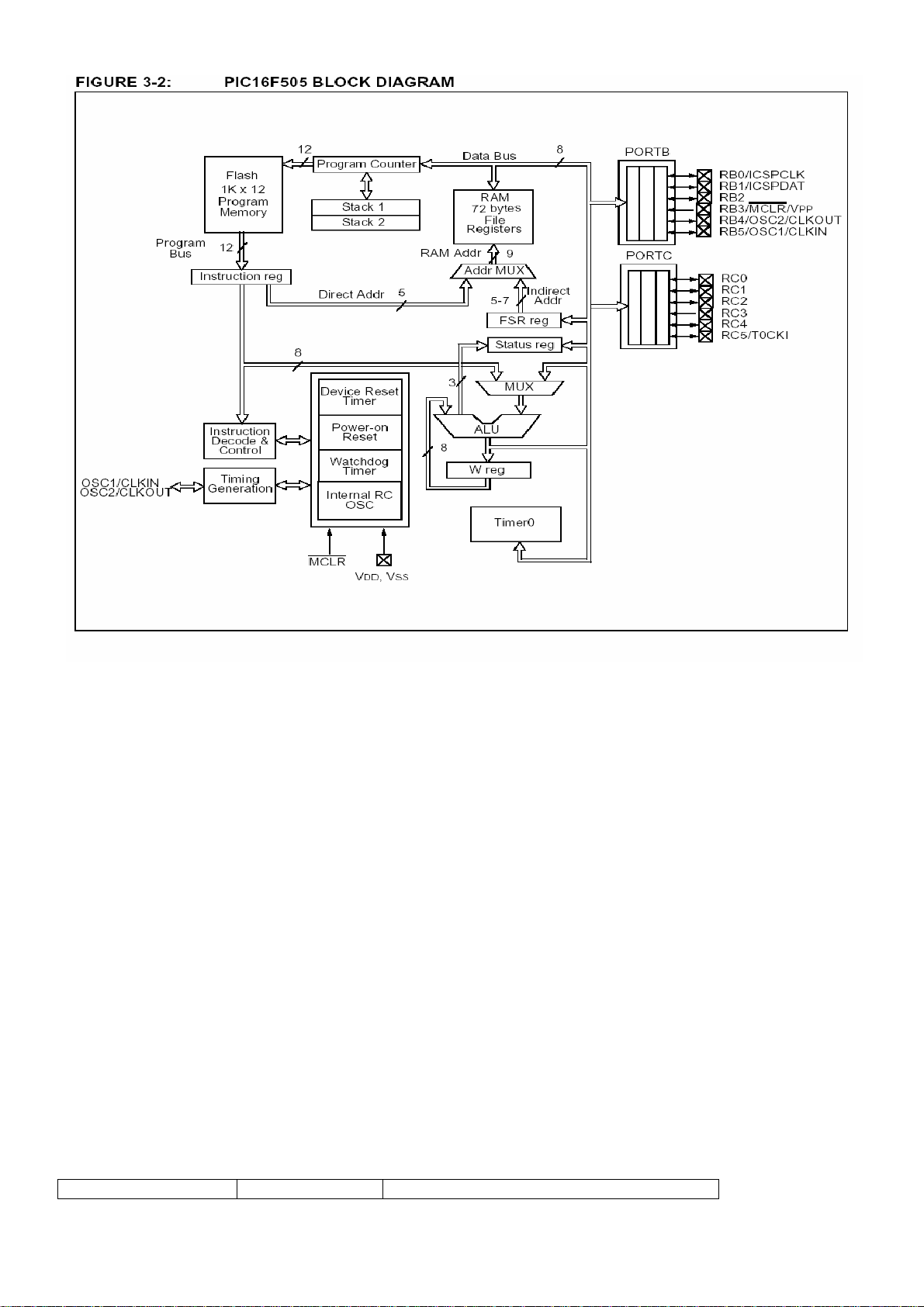
2.3、Standby control CPU(PIC16F505)
Pin number Pin definition Pin function description
1
VDD(+3.3V)
Power
2 RB5/OSC1/CLCKIN NC
3 RB4/OSC2/CLCKOUT LED1 KEYPAD STB output, standby indicator lamp control
4 RB3/MCLP/VPP Input voltage (+5V)when programming or reset input(+5V)
5 RC5 I/O port: POWER OFF1 input, from GM1501 output, inform
PIC16F505 to do off operation.
6 RC4 I/O port: ALARM input, turn on on time enable control.
7 RC3 I/O port: PDP-STB output, standby/on control
8 RC2 I/O port: POWER-STANDBY output,GM1501 to inform
executing off operation by key button.
9 RC1 I/O port: IRIN remote instruction input
10 RC0 I/O port: POWERKEY input, connect to on/off key of k board
directly.
11 RB2 I/O port: connect +3.3V
12 RB1/ICSPCLK programming use
13 RB0/ICSPDAT programming use
14 VSS Ground
8
Page 9
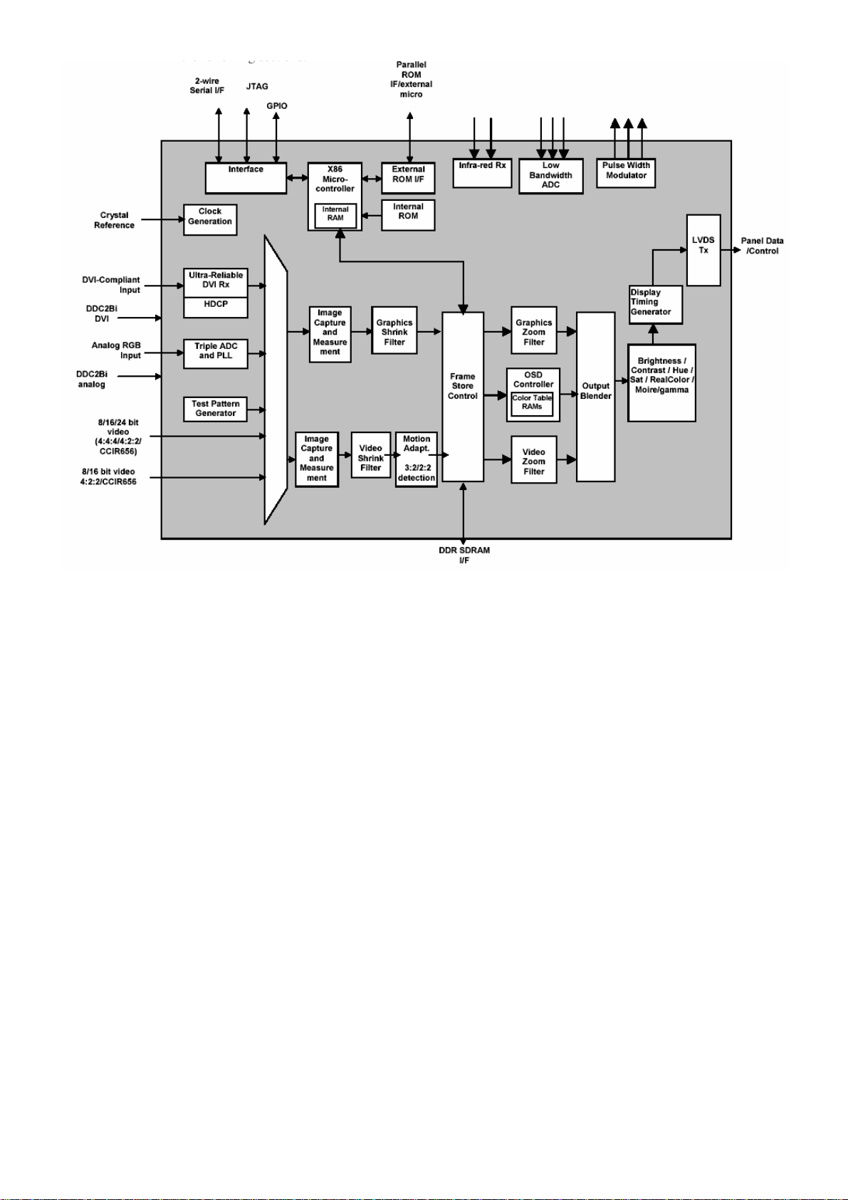
2.4 GM1501
GM1501 is a kind of dual channels image and video processing chip, which is mainly used for LCD displays and TV
integrated products. With the resolution of WUXGA, it not only supports PIP technology, but also include all IC function
of picture snap, process and display clock control. It integrates high speed AD converter, PLL, high reliability DVI
receiver , X86 series microprocessor and LVDS converter inside. Its main e feature as below:
● High quality image zoom function
● Analog RGB signal input interface
● Intelligent input signal mode auto identification;
● Integrated high performance PLL output
● High-reliable self-adaptive DVI input interface;
●4:4:4/4:2:2/CCR656/601 8/16/24bit digital video interface;;
● Embedded adjustment circuit for gain、contrast、brightness、color saturation、hue and skin color;
● technology of reducing EMI power consumption efficiently;
●small angle oblique ripple process;
● High quality video process technology;
● Programmable output format;
● Embedded LVDS transmitter;
● Advanced OSD;
● Embedded micro controller
Pin Description:
Pin Name Description
9
Page 10
Analog signal input port
L3 AVSYNC ADC vertical synchronization signal input
L4 AHSYNC ADC horizontal synchronization signal input
N2 VGA-SCL VGA lock input
N1 VGA-SDA VGA digital input
D1、D2 RED+、RED-
Red analog signal input
C3 SOG Green pedestal synchronization signal
C1、C2 GREEN+、B1、B2 BLUE+、BLUE-
Green analog signal input
Blue analog signal input
A2,B3,E3,D3 ADC3.3 ADC3.3Vpower supply
A3,A4
A5,B4
C4,D4,E1,E2,E4
ADC1.8 ADC1.8Vpower supply
ADC-DGND ADC digital ground
ADC-AGND ADC analog ground
DVI import port
N4
N3
A6,B6 RXC+,RXCA8~A10
B8~B10
DVI-SCL
DVI-SDA
RX0+~RX2+
RX0-~RX2-
DDC interface , serial clock signal
DDC interface ,serial data signal
DVI clock input signal
DVI input port
B11 REXT External interrupt resistance
C6~C11
D6、D8~D10
A7,A11,B5,B7,C7,D7
DVI-3.3 DVI 3.3V power supply
DVI-1.8 DVI 1.8V power supply
DVI-GND DVI ground
D11
Low bandwidth ADC port
C13 LBADC-33 ADC3.3Vpower supply
A12,B12,C12 LBADC_IN1~
ADC analog input channel
LBADC_IN3
D12 LBADC_RETURN Channel analog ground
D13 LBADC-GND Power supply voltage analog ground
OCM bus port
AA1~AA3,Y1~Y3,
W1~W3,V1~V4,
OCMADDR0~
OCMADDR19
Address input output port
U1~U4,T1~T3
AB1~AB3,AC1~AC3,
AD1~AD4,AE1~AE3,
OCMDATA0~
OCMDATA15
Data input output port
AF1~AF3
OCM port control signal
R1,T4,P1,P2
ROM_CSn~
ROM_CS2n
chip selection signal
R2 OCM_REn Read enable signal
R3 OCM_WEn Write enable signal
L1
L2
OCM_INT2
OCM_INT1
Interrupt
M1 OCM_UDO OCM data output
M2 OCM_UDI OCM data input
D25 OCM_TIMER1 OCM timer input
Standard definition video control port
D16 SVCLK SV pixels clock input
C14 SVHSYNC SV horizon synchronization signal input
B14 SVVSYNC SV vertical synchronization signal input
A14 SVODD Scan status input
A17 SVDV SV data input
Standard definition video data port
D14,D15,A15,A16,
B15,B16,C15,C16
SVDATA7~
SVDATA0
SV ITU656 data input
10
Page 11
Video Control Port
A20 VCLK Video pixels clock signal
D19 VHS_CSYNC Video horizonl synchronization signal input
C20 VVS Video vertical synchronization signal input
B20 VODD Scan status input
D20 VDV (VSOG) Video data input
B17 VCLAMP Video clamp enable output
A21,A22,A23,B21,
B22,C21,C22,D21
C17,C18,C19,A18
A19,B18,B19,D18
B23,B24,B25,A24
A25,C23,C24,D24
VGRN7~ VGRN0 Green pedestal signal or Y signal input
VRED7~ VRED0
VBLU7~ VBLU0
Red pedestal signal or V/Cr/Pr signal input
Blue pedestal signal or U/Cb/Pb signal input
Screen Control Port
A26 PPWR Screen power control
B26 PBIAS Screen bias control
D26,C25,C26
PWM2 ~PWM0 Pulse width modulation output
AC7 DCLK Pixels clock output
AC16 OEXTR Connect external LVDS bias resistance
LVDS Port
AE14~AE16,AE19~
AE23,AF13~AF16
A0-~A3-, A0+~A3+
B0-~B3-, B0+~B3+
Low voltage difference data input
AF19~AF23,AF11
AD14,AD11,AE13
AE11,AC11,AF10
AE12,AF12,
LVDS_SHIELD[5] ~
LVDS_SHIELD[0]
AC+,AC-,BC+,BC- Low voltage difference protect input
Low voltage difference protect output
AF20,AE20
Screen Port Power Supply
AD12,AD13,AC12 LVDSB_3.3 LVDS B channel power supply
AC13,AC14,AC15 LVDSB_GND B channel ground
AC20,AC21,AC22 LVDSA_3.3 LVDS A channel power supply
AD19,AC19,AC20 LVDSA_GND A channel ground
AE17 VDDD33_LVDS Analog power supply
AD17 VSSD33_LVDS Analog ground
Clock Composite and Power Supply
G4 XTAL Crystal oscillator interface
F2
VDDD33_PLL,
Digital power supply
H1 VDDD33_SDDS
J1 VDDD33_DDDS
G2 VSSD33_PLL
Digital ground
J4 VSSD33_SDDS
K4 VSSD33_DDDS
F4 VDDA33_RPLL
Analog power supply
G1 VDDA33_FPLL
H3 VDDA33_SDDS
J3 VDDA33_DDDS
F3 VSSA33_RPLL
Analog ground
H4 VSSA33_FPLL
H2 VSSA33_DDDS
J2 VSSA33_DDDS
G3 TCLK Reference clock signal input
K2 ACS_RSET_HD External resistance terminal
System Signal
11
Page 12
K1 RESETn Reset signal
M3,M4 IR0,IR1
P4 MSTR_SCL Master clock output signal
P3 MSTR_SDA Master data output/input signal
R4 EXTCLK External clock input
Frame memory interface
U24,U23 FSCLKp,FSCLKn Differential store clock output
V24,V25 FSRAS,FSCAS Address output
V26 FSWE Write enable terminal
W26 FSCKE Read enable terminal
J24 FSVREF Reference voltage input
K26 FSVREFVSS Reference voltage ground
W25 FSVREF Reference voltage input
W24 FSVREFVSS Reference voltage ground
L26 FSDQS Data filter
F24~F26,G23~G26
H24~H26,J25,J26,
FSDATA31~
FSDATA0
Data input output port
R24~R26,P24~P26
N23~N26,…….
T24,T25,U25,U26 FSDQM3~ FSDQM0 Data output mark
Y26
Y25
AA24~AA26
AB24~AB26,
FSBKSEL1
FSBKSEL0
FSADDR11~
FSADDR0
,
Layer select address
Row and column address output
AC24~AC26
AD24~AD26
E23, F23, H23, J23,
L23,M23,P23, R23,
FS_2.5
2.5V power supply
T23,V23,W23,Y23,
AA23,AB23,AC23
K23 VDDA18_DLL 1.8V power supply
K25 VSSA18_DLL Power supply ground
Digital power
K10,K11,K16,K17,
CORE_1.8 1.8V power supply
L11,L16,T11,T16,
T17,U10,U11,U16,U17
D23, W4,Y4, AA4,
AB4,AC4,AC6,D17,
IO_3.3
3.3V power supply
D22,AC8,AC10
K12,K13,K14,K15,
L10,L12,L13,L14,
D_GND
L15,L17,M10,M11,
M12,M13。。。。。。
A1,AC,D5,AC17,
K3,F1
NO_CONNECT
GM1501internal block Diagram:
Power ground
NC
12
Page 13
2.5. Brief Introduction of TDA8759:
TDA8759 is a triple 8-bit video converter interface. Sample rate is up to 81 Mbps .The IC can convert analog RGB
signal into a 24bit RGB digital signal o, or converts analog YUV or YCbCr signal into a YUV or RGB digital.
The IC supports resolutions from 480i and VGA to HDTV and XGA.
● Triple 8-bit Analog-to-Digital Converter (ADC)
●Three independent I2C selectable analog video sources
●Auto detect to interlace scan video signal
●1.8Vand 3.3Vsupplies
● Low gain temperature shift
●Output format support RGB 4:4:4, YUV 4:4:4, YUV 4:2:2 ,CCIR 656 or YUV 4:2:2 ;
●I²C bus control
●Programmable clock phase correct circuit inside
●100 MHz Amplifier bandwidth
●Integrated PLL distribution
●Power-Down mode
TDA8759 internal schematic Diagram:
13
Page 14
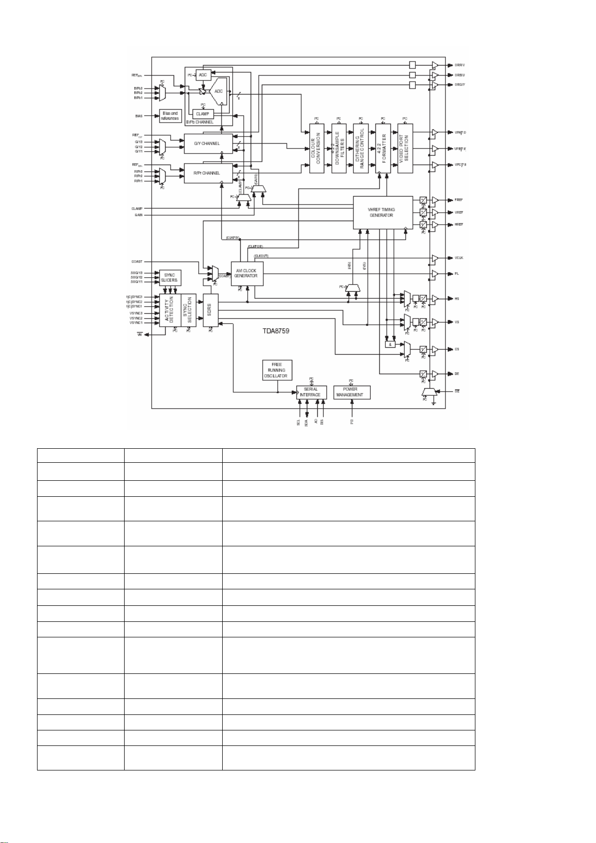
Pin Description:
Pin Name Description
1 HREF Horizon reference output
2 VCLK Video clock output
3,13,21,29,
VDDO Video port output supply voltage
37,45,164
4,14,22,30
OGND Video port output ground
38,46,165
7,8,9,10,
VPA0~VPA7 Video port A
15,16,17,18
11,116,130,132 VDDC Power supply port
12,117,159 CGND Ground
23~28,31,32 VPB0~VPB7 Video port B
35,36,39~44 VPC0~VPC7 Video port C
47,53,57,58,55
AGND Analog ground
60,66,70,71,75
81,83,85,86,
48,54,59,61,67
VDDA Power supply port
69,76,82,85,87,88
49 REFB/Pb Blue/blue-chrominance channel reference input signal
52,51,50 B/Pb1~ B/Pb3 Blue/blue-chrominance channel analog input
56 BIAS Bias input
62 REFG/Y Green/luminance reference input
14
Page 15
65,64,63 G/Y1~G/Y3 Green/luminance analog input
74,73,72 SOG/Y1~SOG/Y3 Sync on green//luminance input
77 REFR/Pr Red/red-chrominance channel reference input
80,79,78 R/Pr1~ R/Pr3 Red/red-chrominance channel analog input
89~92,97~101
TST0~TST17 Reserved for test
112,121,122,
124,125,160~163
93 PD Power-down control input
94 OE Output enable signal input
96 A0 I²C bus address control signal input
102 COAST PLL control signal input
103 GAIN Gain input
104 CLAMP Clamp input
105~107 VSYNC1~VSYNC3 Vertical synchronization signal input
108~110 H(C)SYNC1~
H(C)SYNC3
Horizon (color)synchronization signal input
111 CKEXT External clock input
113 TCLK Reserved for test
114 DIS I²C bus disable control signal input
118 SDA I²C bus data input/output
119 SCL I²C bus clock input
120,126,127,131
IGND Input digital ground
133,142,148,
123,138,139,145
VDDI Input digital supply voltage
151,157
166 PL PLL disable signal output
167 DE Data enable output
168 HS Horizon synchronization signal input
169 VS vertical synchronization signal input
170 CS Color synchronization signal output
171 ORR/V Red / chrominance ADC output
172 ORB/U Blue /chrominance ADC output
173 ORG/Y Green / chrominance ADC output
174 VAI Video dynamic indication output
175 FREF Scan signal output
17 VREF Vertical reference input
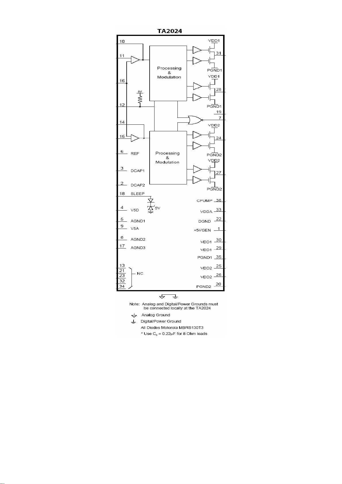
2. 6、TA2024 general:
The TA2024 is a 10W/ch continuous average two-channel Class-T Digital Audio Power Amplifier IC using
Tripath’s proprietary Digital Power Processing™ technology. Class-T amplifiers offer both the audio fidelity of
Class-AB and the power efficiency of Class-D amplifiers. It has below feature:
z Mute control
z Temperature protect circuit
z Low noise switch
z Power supply:12V
Pin Function Descriptions:
Pin(s) Name Function
2, 3 DCAP2, DCAP1 Charge pump switching pins
4, 9 V5D, V5A Digital 5VDC, Analog 5VDC
5, 8, 17 AGND1, AGND2, AGND3 Analog Ground
6 REF Internal reference voltage
15
Page 16
7 OVERLOADB A logic low output indicates the input signal
has overloaded the amplifier
10,14
OAOUT1, OAOUT2 Input stage output pins.
11, 15 INV1, INV2 Single-ended inputs
12 MUTE Mute control
16 BIASCAP Input stage bias voltage
18 SLEEP Sleep mode control
19 FAULT A logic high output indicates thermal
overload
20, 35 PGND2, PGND1 Power Grounds (high current)
22 DGND Digital Ground
24, 27; 31, 28 OUTP2 & OUTM2; OUTP1
Bridged outputs
& OUTM1
25, 26, 29, 30
VDD2, VDD2 , VDD1,
VDD1
Supply pins for high current H-bridges,
nominally 12VDC.
13, 21, 23, 32, 34 NC Not connected
33 VDDA Analog 12VDC
36 CPUMP Charge pump output
1 5VGEN Regulated 5VDC source used to supply
power to the input section (pins 4 and 9).
TA2024 Block Diagram:
16
Page 17
2.7.Brief Introduction to SM5302AS :
The SM5302AS is a 3-channel video buffer with built-in 5
type, and output gain switching can be controlled using a IIC control bus, and the IIC slave address can be set by ADS(3-state
input) to allow a maximum of three devices to be used simultaneous.
FEATUES:
th -
order low pass filter. The cutoff frequency, signal input
● supply voltage:analog:4.75V~5.25V; digital:3.0~5.5V
● 2-system input multiplexer function(switchable using IIC or MUXSEL input)
● Filter bypass mode function for display specifications up to SVGA resolution.
●
Video input pins can be independently set to sync-tip clamp/bias/direct input.
● Output gain switching: 0/6dB
● Output sag compensation circuit built-in.
●
Half fc mode switch function(CH-2,CH-3) suitable for digital component signals.
17
Page 18
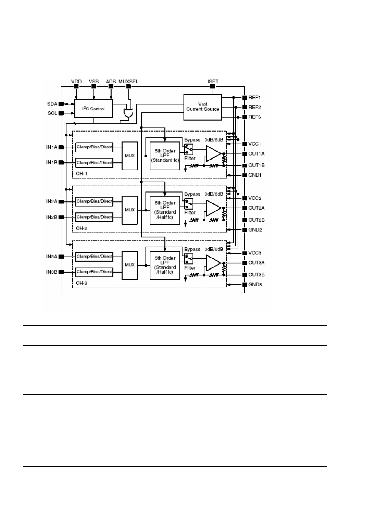
● IIC interface control: slave address:90h,92h or 94h(up to three devices can be used simultaneously,selected by ADS
input); data transfer rate: fast mode(up to 400kbps)
● Cutoff frequency:4.8 to 43MHz variable
SM5302AS Internal Diagram:
Pin Description:
Pin Name Description
1 REF1 Internal reference voltage 1
2 VDD
3 SDA
4 SCL
5 Vss
Digital supply(3.0~5.5V).
IIC data signal input/output
IIC clock signal input
Digital ground
6 MUXSEL Input multiplexer switch control
7 ADS IIC slave address select(three state input)
8 IN1A Video signal input 1(CH-1, input A)
9 IN1B Video signal input 1(CH-1, input B)
10 ISET
Internal current-setting resistor(Riset) connection(1.8K
11 IN2A Video signal input 1(CH-2, input A)
12 IN2B Video signal input 1(CH-2, input B)
13 IN3A Video signal input 1(CH-3, input A)
14 IN3B Video signal input 1(CH-3, input B)
18
Ω)
Page 19
15 GND3 Analog ground(CH-3)
16 Out3B Video signal output(CH-3,for sag compensation)
17 Out3A Video signal output(CH-3)
18 VCC3
19 GND2
Analog supply(CH-3)(4.75 to 5.25V).
Analog ground(CH-2)
20 Out2B Video signal output(CH-2,for sag compensation)
21 Out2A Video signal output(CH-2)
22 VCC2 Analog supply(CH-2)(4.75 to 5.25V).
23 GND1 Analog ground(CH-1, Vref)
24 Out1B Video signal output(CH-1,for sag compensation)
25 Out1A Video signal output(CH-1)
26 VCC1 Analog supply(CH-1,Vref)(4.75 to 5.25V).
27 REF3 Internal reference voltage 3
28 REF2 Internal reference voltage 2
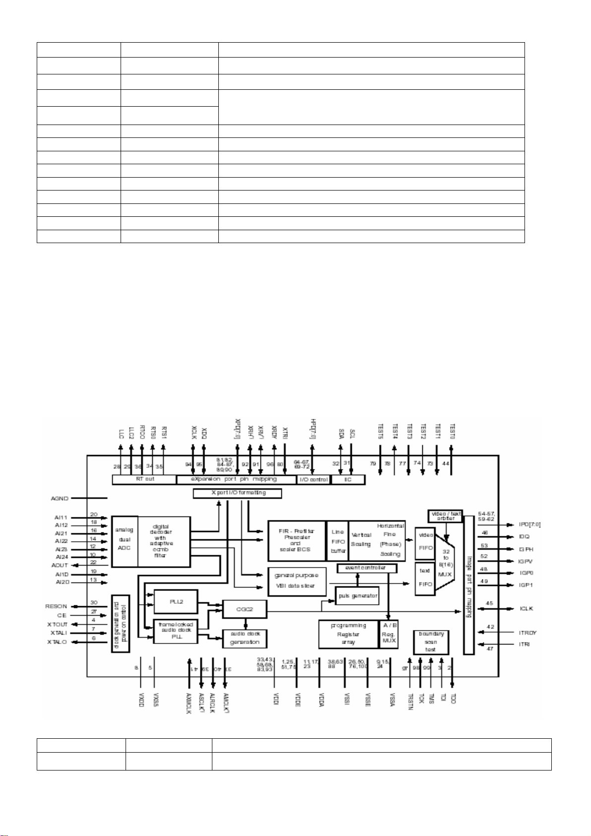
2.8. Brief Introduction to SAA7115:
The SAA7115 is a video capture device for various applications ranging from small screen products like e.g. digital set top
boxes, personal video recording applications to big screen devices like e.g. LCD projectors due to it’s improved comb filter
performance and 10 bit video output capabilities.
●Six analog inputs, internal analog source selectors;
●Two improved 9 Bit CMOS analog-to-digital converter in differential CMOS style;
●
Automatic Clamp Control (ACC) for CVBS, Y and C;
●Enhanced Horizontal and vertical Sync Detection;
●
PAL delay line for correcting PAL phase errors;
●
Automatic TV/VCR detection;
SAA7115 Internal Diagram:
Pin Function:
Pin Name Description
1,8,11,17,23,25,33 VDD Supply voltage port
19
Page 20

43,51,58,68,75,83
93
2 TDO
3 TDI
4 XTOUT
Test Data Output for Boundary Scan Test (2)
Test Data Input for Boundary Scan Test (with internal pull-up)(2)
crystal oscillator output signal, auxiliary signal
6 XTALO
7 XTALI
24.576 (32.11) MHz crystal oscillator output; not connected if XTALI is driven
by an external single-ended oscillator.
Input terminal for 24.576 (32.11) MHz crystal oscillator or connection of external oscillator
with TTL compatible square wave clock signal.
6 VXDD Crystal oscillator power supply
10,12,14,16 AI21~AI24 Analog signal input
13 AI2D
differential input for ADC channel 2 (pins AI24, AI23, AI22, AI21)
differential input for ADC channel 1 (pins AI12, AI11)
19 AI1D
20 AI11
18 AI12
5,9,15,21,24,26,38
50,63,76,88,100
AGND
VSS
22 AOUT
27 CE
28 LLC
29 LLC2
30 RESON
31 SCL
32 SDA
34 RTS0
35 RTS1
analog input 11
analog input 12
ground
Analog test output (do not connect)
Chip Enable or RESET input (with internal pull up)
line-locked system clock output (27 MHz nominal), for backward compatibility,
do not use for new applications
line locked clock/2 output (13.5 MHz nominal) for backward compatibility, do
not use for new applications
RESet Output Not signal
IIC serial clock line (with inactive output path)
IIC serial data line
real time status or sync information, controlled by subaddr. “11h and 12h”
RTS1 35 O real time status or sync information, controlled by subaddr. “11h and 12h”
36 RTCO Real time control output
37 AMCLK Audio master clock output
39 ASCLK Audio serial clock output
40 ALRCLK Audio lift/right clock output
41 AMXCLK Audio master external clock input
42 ITRDY Target ready input, image port(with internal pull up)
45 ICLK
46 IDQ
47 ITRI
48 IGP0
49 IGP1
52 IGPV
53 IGPH
54~57,59~62 IPD0~IPD7
64~67,69~72 HPD0~HPD7
80 XTRI
81,82,84,85,
XPD0~XPD7
89,90,86,87
clock output signal for image-port, LCLK of LPB image port mode, or optional
asynchron. backend clock input
output data qualifier for image port (optional: gated clock output)
image-port output control signal, effects all I-port pins incl. ICLK, enable and active
polarity is under software control (bits IPE in subaddr. “87”) output path used for Testing:
scan output
general purpose output signal 0; image-port (controlled by subaddr. “84”,”85”)
general purpose output signal 1; image-port (controlled by subaddr. “84”,”85”),
same functions as IGP0
multi purpose vertical reference output signal; image-port
(controlled by subaddr. “84”,”85”)
multi purpose horizontal reference output signal; image-port
(controlled by subaddr. “84”,”85”)
image port data output
Host port data I/O, carries UV chrominance information in 16 bit video I/O modes
X-port output control signal, effects all X-port pins (XPD[7:0], XRH, XRV, XDQ
and XCLK) enable and active polarity is under software control (bits XPE in subaddr.
“83”)
expansion-port data
expansion-port data
20
Page 21

91 XRV
92 XRH
94 XCLK
95 XDQ
96 XRDY
vertical reference I/O expansion-port:
In ten bit video output mode: this signal represents the video bit 0.
horizontal reference I/O expansion-port:
In ten bit video output mode: this signal represents the video bit 1.
clock I/O expansion port
data qualifier I/O expansion port
task flag or read signal from scaler, controlled by XRQT (subaddr. 83H)
97 TRSTN
98 TCK
99 TMS
Test Reset Not for Boundary Scan Test (with internal pull-up); for board design
without Boundary Scan connect TRSTN to ‘ground’
Test Clock for Boundary Scan Test (with internal pull-up)(2)
Test Mode Select for Boundary Scan Test or Scan Test (with internal pull-up)(2)
(1)
2.9.Brief Introduction to UOC (Ⅲ TDA15063H):
The UOCIII series combines the functions of a Video Signal Processor (VSP) together with a FLASH embedded
TEXT/Control/Graphics -Controller (TCG -Controller) and US Closed Caption decoder.
●DVB/VSB IF circuit for preprocessing of digital TV signals;
●
Video switch with 3 external CVBS inputs and a CVBS output;
●Automatic Y/C signal detector;
●Adaptive digital (4H/2H) PAL/NTSC comb filter for optimum separation of the luminance and the chrominance signal
●Picture improvement features with peaking (with switchable center frequency, depeaking, variable positive/negative peak
ratio, variable pre-/overshoot ratio and video dependent coring), dynamic skin tone control, gamma control and blue and black
stretching. All features are available for CVBS, Y/C and RGB/YP
BPR signals.
The mono intercarrier sound circuit has a selective FM-PLL demodulator which can be switched to the different FM sound
frequencies (4.5/5.5/6.0/6.5 MHz). The quality of this system is such that the external band-pass filters can be omitted. In the
stereo versions of UOC
III the use of this demodulator is optional for special applications.
Normally the FM demodulators of the stereo demodulator/decoder part are used (see below).
●The FM-PLL demodulator can be set to centre frequencies of 4.72/5.74 MHz so that a second sound channel can be
demodulated. In such an application it is necessary that an external band-pass filter is inserted.
●The vision IF and mono intercarrier sound circuit can be used for the demodulation of FM radio signals. With an external FM
tuner also signals with an IF frequency of 10.7MHz can be demodulated. For the QIP90 versions this is valid only for the
“stereo” versions
●Built-in adaptable brightness delay circuit
●switchable brightness signal transmission rate
Pin Description:
Pin Name Description
1,2,12,18,28,40
VSS,GND ground
68,81,89,92,95,101
121,125
3,4,45,69,82,88,90,
VDD Power supply
91,93,94,96,100,
110,117,118,124
5 VREF_POS_LSL
SDAC input signal
6 VREF_NEG_LSL+HPL
7 VREF_POS_LSR+HPR
8 VREF_NEG_HPL+HPR
9 VREF_POS_HPR
10 XTALIN Crystal oscillator input
11 XTALOUT Crystal oscillator output
13 VGUARD/SWIO
14 DECDIG
15 VP1
V-guard input / I/O switch
decoupling digital supply
decoupling digital supply
21
Page 22

16 PH2LF
phase-2 filter
phase-1 filter
17 PH1LF
19 SECPLL
20 DECBG
21 EWD/AVL
22 VDRB
SECAM PLL decoupling
bandgap decoupling
East-West drive output or AVL capacitor
vertical drive B output
vertical drive A output
23 VDRA
24 VIFIN1
25 VIFIN2
27 IREF
29 SIFIN1/DVBIN1
IF input 1
IF input 2
reference current input
SIF input 1 / DVB input 1
30 SIFIN2/DVBIN2
31 AGCOUT
32 EHTO
33 AVL/SWO/SSIF/REFO/REFIN
34 AUDIOIN5L
tuner AGC output
EHT / overvoltage protection input
Automatic Volume Levelling / switch output reference output / external
reference signal DVB operation
audio-5 input (left signal)
audio-5 input (right signal)
35 AUDIOIN5R
36 AUDOUTSL
37 AUDOUTSR
38 DECSDEM
39 QSSO/AMOUT/AUDEEM
audio output for SCART/CINCH (left signal)
audio output for SCART/CINCH (right signal)
decoupling sound demodulator
QSS intercarrier output / AM output / deemphasis
41 PLLIF PLL filter
42 SIFAGC/DVBAGC
43 DVBO/IFVO/FMRO
AGC sound IF / internal-external AGC for DVB applications
Digital Video Broadcast output / IF video output
44 DVBO/FMRO
46 AGC2SIF
47 VP2
48 IFVO/SVO/CVBSI
49 AUDIOIN4L
50 AUDIOIN4R
AGC capacitor second sound IF
2nd supply voltage TV processor (+5 V)
video output / selected CVBS output / CVBS
audio-4 input (left signal)
audio-4 input (right signal)
51 CVBS4/Y4 CVBS/Y input
52 C4
53 AUDIOIN2L/SSIF
54 AUDIOIN2R
56 AUDIOIN3L
57 AUDIOIN3R
chroma-4 input
Audio input
30 AUDOUTLSL
61 AUDOUTLSR
62 AUDOUTHPL
63 AUDOUTHPR
58 CVBS3/Y3 CVBS/Y input
59 C2/C3
chroma-2/3 input
55 CVBS2/Y2 CVBS/Y input
64 CVBSO/PIP CVBS/PIP signal output
65 SVM
66 FBISO/CSY
67 HOUT
scan velocity modulation output
flyback input/sandcastle output or composite H/V
horizontal output
22
Page 23

70 VIN (R/PRIN2/CX)
71 UIN (B/PBIN2)
72 YIN (G/YIN2/CVBS-YX)
73 YSYNC
74 YOUT
75 UOUT (INSSW2)
76 VOUT (SWO1)
77 INSSW3
78 R/PRIN3
79 G/YIN3
80 B/PBIN3
83 BCLIN
85 RO
86 GO
87 BO
97 INT0/P0.5
98,99,102~109
111~116,119,120
122,123,126~ 128
P0.0~ P0.4
P1.0~P1.7,P2.0~P2.5,
P3.0~P3.3
V-input for YUV interface
U-input for YUV interface
Y-input for YUV interface
Y-input for sync separator
Y-output (for YUV interface)
U-output for YUV interface
V-output for YUV interface
3rd RGB / YPBPR insertion input
3rd R input / PR input
G input / Y input
3rd B input / PB input
beam current limiter input
Red output
Green output
Blue output
external interrupt 0 or port 0.5 (4 mA current sinking direct drive of LEDs)
Data port
UOCⅢ inside block diagram:
23
Page 24

PartⅢ:Analysis on Signal Process Flow of PT4216 and key point test data
This chapter mainly introduces receiving and process of picture and sound signal of PDP TV and
system control procedure, supply system of unit.
1. Picture signal process Flow
IF signal which is demodulated by main tuner is sent by AV board module into video decode chip UOC for Ⅲ
decoding ,then switched with signal from AV/S jack by internal electric switch of UOCⅢ, then the output analog video
signal is sent into analog-to-digital converter TDA8759HV/8/C1 for A/D transforming to produce R、G、B digital signals,
format converted by GM1601/GM1501,then, GM1601/GM1501 transform the different input formats into the uniform
up-screen signal format.
The signal demodulated by sub tuner is directly sent into sub-picture video decoder SAA7115HL/V1 for video
decoding and A/D conversion,then sent into GM1601/GM1501 again to do format transforming, the output up-screen
signal is used for sub-picture display.
The alternative PC、 HDTV(YPBPR) and DVI signals are sent directly into GM1601/GM1501 for processing to
form uniform up-screen signal.
2 Sound process flow:
TV sound: RF signal is demodulated by main tuner and output SIF signal. SIF input to UOCⅢ to demodulate and
wow process. Output audio signal to dual channel class-T digital audio power amplifier IC TA2024 on power amplifier
board. At last is sent to speaker.
AV sound: audio signal from AV is sent to UOCⅢ for processing directly ,then be amplified by power amplifier IC
TA2024 to drive speaker.
PC、DVI、YPbPr sound: Signal is processed by UOCⅢ on main board and amplified by TA2024 on power amplifier
board after it is strobed by MC74LVX4052DR2.
3、System control process:
After connect the AC power input (we use 3 pins power jack,the GND pin must ground well).First of all ,standby
power on power board works,signal main board obtains 5V-ST power supply,then 5V-ST power is regulated to 3.3V by
U900 on main board. At this time, standby CPU PIC16F505 begin to work, and LED lamp indicates red. After user gives
key or remote on instruction, the 7
power board to turn on, AC power on panel turns on. Each group DC power on power board is normal and output
to main board. GM1501 on main board reset normally under A702 IC control, then finish system initialization.
Meanwhile finish up-screen signal control. LED indicator turns green. It is proved system control normally.
3.1、When choice VGA mode by remote control box ,GM1501 controls TDA8759 enable by I
them work in low power consumption mode,which can save power and reduce interfere。At the moment GM1501 output
Sel_HsVs signal to set PI5V330 in VGA input channel. If there is VGA signal input, directly into GM1501
to detect and process, output is transformed to signal suitable for PDP panel. If no VGA signal input, GM1501 can’t
detect horizon and vertical sync. Signal. PDP panel display PC icon at left upper corner of screen under GM1501 system
control. Other area of panel display black screen. If no input after 60 sec, it hints to enter “save power mode”.At the
moment ,examines VGA signal ceaselessly,so it can be awaken automatically in VGA mode. It is said that when VGA
signal inputs, it can work normally from standby state
3.2、When in TV/AV /YCbCr mode by remote control box,GM1501 controls UOC3 by I
signal inputs,PDP panel display normally;if no video signal input,under the control of GM1501,PDP panel displays
blue background,if no signal after 15 mins,power off automatically and into standby state. It can not be awaken
automatically。
3.3、When in DVI(digital RGB) mode by remote control box,GM1501 controls TDA8759 enable by I
them work in low power consumption mode. When DVI signal inputs, display video;if no DVI signal,GM1501 can’t
detect horizon and vertical sync. Signal. PDP panel display DVI icon at left upper corner of screen under GM1501
system control. Other area of panel display black screen. If no input after 60 sec, it hints to enter “save power
th
pin of PIC16F505 sends PDP-STB high level signal to control relay T802 on
2
C bus,let
2
Cbus. When video
2
C bus,let
24
Page 25

mode”.At the moment ,examines DVI signal ceaselessly,so it can be awaken automatically in DVI mode. It is said that
when DVI signal inputs, it can work normally from standby state
4、Power supply system:
Power board has seven ways voltage output all together. They are 34V, 12V, 12VAU,A6V,D6V,D3.3V and
5V. 34V regulated by IC upc574 is provided to tuner for tuning voltage. 12VAU is provided to audio power amplifier.
A6V、D6V is changed 5V by LDO(example TA4805F),used by different circuit network. D3.3V is changed 2.5V and
1.8V by LDO(example LM1117,LM1084 etc.),used by different IC. 5V power supply is used by MCU
(PIC16F505),infrared receiver and k board assembly etc. when standby.
When standby, except above 5V supply, other powers are all off.
4.1 Main power form and power branch:
4.1.1、5V-ST power branch
XP 915
5th pin
5V-ST
4.1.2、D6V power branch
XP900
11th pin
D6V
U913、 U923
TA4805F
U900
LM 11 17-3.3
XP910
1th,3th
pin
3.3VPU LL
K board connection
VCC5A
VCC5A
+5VB
15 th , 69 th pin
U0C3 SCL, UOC3 SD A,
UOC SW1, UOC3 SW2,
SAW SW port power
supplied by pull-up resistor
3.3VPULL
3.3VP U LL
K board
assem bly
U201 U0C3
UP7
LM 1117-1.8
U901 PIC16F505
1th pin
U 902 P C F8563
8th pin
3
Remote control
board assembly
J171 6th? 7th pin
V1_8ANA
U201 UOC3
36th pin
U201 UOC3
3th, 118th, 124th
pin
UP1
LM 1117-3.3
U903
LM 1117-2.5
LM 1117-1.8
V_3.3A
+ 2.5V_DD R
UP7
U201 UOC3
4th, 7th, 80th,
94th, 110th pin
V1_8V1
U600 MT46V2M32LG-4
2th, 8th, 14th, 22th, 59th, 67th, 73th,
79th, 86th, 95th, 15th, 35th, 65th,
96th, 58th pin
25
Page 26

4.1.3、VDD(3.3V) power branch
+3. 3V_DVI
+3.3V_PLL
+3. 3V_LVDS
+3.3V_LVDSA
+3.3V_LVDSB
U700 GM1501
C6, C8, C9, C10, C11, B11 pin
U700 GM1501
G3, G4, J1, J3, H1, H3, G1, F2, F4
pin
U700 GM1501
AE17 pin
U700 GM1501
AC21, AC22, AD20 pin
U700 GM1501
AD12, AD13, AC12 pin
G3, G4 crystal oscillator X700
external connect capacitor
XP900
8th、9th
pin
PDP-D3.3V
+3. 3V_I/ O_BGA
+3.3V_ADC
U914
LM1117-1.8
+3. 3V_L BADC
+3. 3V_DI G
U700 GM1501
D17, D23, AC4, AC6, AC10, D22, AA4, W4, AB4,
Y4 pin
U700 GM1501
C13 pin
U801 29LV800BT
37 pin
U700 GM1501
A2, B3, D3, E3 pi n
U700 GM1501
K17, U17, U11, L16, T16, T17, L11, K10, K16, T11,
U16, U10, K11, K23 pin(+1. 8V_CORE),A3, A4 pin
(+1. 8V_ADC),D6, D8, D9, D10(+1 .8V_DVI )
4.1.4、A6V power branch
U912
IRF7134
PDP_D3.3V_1
U400 TDA8759
(+3.3V_DEC,+3.3V
_SW)
26
Page 27

XP905
1th pin
U915
TA 4805F
+5_A N G
U309( 16th pin), U 305( 1 8 th , 2 2 th ,
26th pin) , U 3 0 7 ( 16th pin), U 306
( 16th pin) and each port audio input
circuit bias supply
4.1.5、A12V power branch
XP900
PDP_D12V
5th pin
+5V
+12V_DC
+12V_3A
U308( 16th pin), U 311( 14th pin), X P900
( 7th、 8th pin) and G P IO port pull-up
pow er supply
SCOL, SCOR audio
output circuit power
supply
U916
TA4808F
U5 TDA9178T
20th pin
The Pin Voltage of regulator on Main Board
4.2
position type PIN1(V) PIN2(V) PIN3(V) PIN4(V) PIN5(V)
UP7 LM1117-1.8V 0 1.8 5 1.8
UP1 LM1117-3.3V 0 3.3 5 3.3
U913 4805F 6 0 5
U923 4805F 6 0 5
U916 78M08 12 0 8
U403 LM1117-1.8V 0 1.8 3.3 1.8
U915 4805F 6 0 5 0
U903 LM1117-2.5 0 2.5 5 2.5
U914 LM1117-1.8V 0 1.8 3.3 1.8
U900 LM1117-3.3V 0 3.3 5 3.3
4.3 Main Components and Socket Locations and Definitions on main board module:
27
Page 28

O
6
J
M
20
5
4
N
3
I
7
F
9
10
E
8
1
Socket definition
number name Connected object Function description
6 XP915 Power board Standby power and on/off control
11 XP907 Power amplified board Left and right channel sound output
5 J171 Remote control board
3 XP909 K board
4 XP910 K board
1 XP926 AV board
2 XP927 AV board
7 CN900 PDP pannel LVDS cable to panel
10 XP936 PDP pannel Timing control signal of power board of Panel
8 XP900 Power board
9 XP905 Power board
12 XP922 AV output
13 XP923 AV1 input
14 XP935
15 XP925 YPbPr audio input
16 XP924 YPbPr high definition
17 AVP303 DVI audio input
18 CN300 DVI input
19 AVP300 VGA audio input
20 CN301 VGA input
AV 2 (S)input
signal input
G
11
D
C
A
PDP-D6V,PDP-D3.3V,PDP-D12V input
PDP-A6V,PDP-A12V,PDP-12VAMP,PDP-VT33V input
B
2
19
L
18
K
17
H
16
15
14
13
12
Main components description
number name
C U201
E U400
F U402
type
TDA15063H-N1B06557
TDA8759HV/8/C1 Video signal A/D converter
SAA7115HL/V1 Sub channel video decoder
Function description
Audio and video decoder
28
Page 29

G U600 MT46V2M32LG-4 Frame buffer
I U700
H U305
J U801
D U5
B K202
A K201
N U901
O U902
M U306
L U302
K U303
5、Key point waveform
5.1
RF input full color stripe signal, waveform of the 18
and the 10
th
pin of SAA7115 is like this:
GM1601/GM1501-BD Video processor
SM5302AS-G-ET High definition signal filter
AM29LV800DT-70EC
TDA9178T/N1 Video signal picture quality improvement
K9352N SAW filter
K7262N SAW filter
PIC16F505 Standby control CPU
PCF8563 Real time clock counter
FSAV330QSCX Select switcher
24LC21A T/SN EEPROM
24LC21A T/SN EEPROM
Flash,save TV control program
th
pin of sub tuner UT921, the 8th pin of XP926
RF input full color stripe signal, the waveform of Pin85,Pin86,Pin87 of U201 output R,G,B
5.2
signal ,the E pin of Q171,Q172,Q173 is like this:
29
Page 30

5.3、RF input full color stripe signal, the waveform of I²C bus clock signal UOCIII_SCL, the 98th pin of
U201,the 11th pin of U5,the 4th pin of main tuner UT920, the 4th pin of sub tuner UT921,the 1th pin of
XP926 is like this:
5.4、RF input full color stripe signal, the waveform of I²C bus clock signal UOCIII_SDA, the 99
th
pin of
U201,the 14th pin of U5,the 5th pin of main tuner UT920, the 5th pin of sub tuner UT921,the 2th pin of
XP926 is like this:
30
Page 31

5.5、 RF input full color stripe signal, the waveform of UOC vertical sync signal,
the 22th pin of U201,the 105th pin of U400 is like this:
5.6、RF input gray ladder signal, the waveform of the 18
th
the 10
pin of SAA7115 is like this:
31
th
pin of sub tuner UT921,the 8
th
pin of XP926,
Page 32

7、The 1KHz sound signal input, the waveform of the 60th 、61
is like this:
th
pin of U201, the 6th、8th pin of XP907
32
Page 33

PartⅣ:Typical troubleshooting process flowchart of PT4216
one、red led does not light
red led does not light
Check K board
yes no
iack XR900 11 pin
3.3V power
Y
N
yes no
Check PCB
connect
Check
resistor RK2 、
light diode
VDK1
Check if 6th,7th pin
of jack J171 on main
board there is 3.3V power
supply
1、Check whether FB927 on main
board is normal or not.
2、Check if U900 on main board
work normally or not
Check mainboard jack XP915
5 pin 5V power
Check standby
circuit of power
board and power
jack AC 220V
input
33
Page 34

two、The red led lights,but doesn’t turn to yellow after power on and black display
1. Check
connector
2.Check PDP
power module
Check bus circuit
and PCB wire
Power on, check XP915
3th pin PDP-STB signal is
high level 3.3V or not?
yes
Check XP900 PDP-
no
D6V, PDP-3.3VVDD is
normal or not
abnorma
l
I2Cbus
yes
Yes
no
Check U901,
U902 output
voltage is normal
or not
Yes
Check X700
14.318M crystal is
normal or not
Yes
Check U700
GM1501 RESET
pin voltage is
normal or not
Check U901,U902
No
power supply and
peripheral circuit
No
No
Check reset circuit
Change X700
crystal
A702
normal
1. Check GM1501 power circuit
2. Check GM1501 C25,D26 output voltage
is normal or not
3.Check GM1501 peripheral circuit
34
Page 35

three、The red led lights,turns to green color after power on but display black screen
35
Page 36

four、no picture:
No picture only VGA
or YPbPr mode
Check GM1501 L4?
L3 pin horizon and
vertical sync waveform
is normal or not?
Yes
1? Check R,G,B input
waveform of
GM1501 is ok or not
2? Check U305,
U306, U307 is ok or
not
Check U310 input
and output sync.
waveform of sync
No
regulating circuit
is normal or not
Check VGA jack
input
abnorma
l
Check if there is anyone
normal picture to display
when source switches
output
abnormal
Check power supply
and peripheral circuit of
sync regulating circuit
are normal or not ?
Other part is on
next page
No picture only
DVI
1? Check signal source
2? Check DVI socket
yes
Use oscillograph
to check GM1501
DVI LVDS signal
input is normal or
not
36
Page 37

if there is one
state to display
when switch the
source
TV, AV, S-VIDEO,
all no picture
check U400
TDA8759 horizon
and vertical sync.
And clock ok or
not
check TDA8759 horizon
and vertical sync. And
clock output is normal
or not
No
check TDA8759 power
and peripheral circuit;
change TDA8759
only AV no
picture
check AV board
connector
joint well
check UOC3 AV
I/O is ok or not?
input ok, but output
abnormal
check UOC3 and
TDA9178 power,
bus;
no picture only S-
video
check S-video
connector
Yes
check UOC3 S-
video I/O is ok or
not
Input ok,but output
abnormal
check UOC3 and
TDA9178 power,
bus;
only TV no picture
check UOC3 31th,41th pin
voltage and peripheral
component is ok or not
check TAD5-
C2F21RW power,
bus and SAW filter
circuit
check and change
TAD5-C2F21RW
37
Page 38

Five、no sound or low sound volume
no sound or low
sound volume
check XP302、
XP303 connection
of power amplifier
board;sound box
connection line
check XP302、
XP303 output signal
check TA2024 input
signal
check UOC3 output
signal
check UOC3 input
signal
other source
check sound input
no input
normal
Yes
TV
Yes
check TA2024
power、mute
control
check UOC3 output coupling
circuit R219、R220、XP907
check 20th,30th pin
SIF input
Yes
check UOC3
power、clock、
reset、bus
normal
normal
check and change
TA2024
check TAD5-
C2F21RW output
SIF signal
normal
check SIF filter
amplifier circuit
abnormal
check and change
TAD5-C2F21RW
check signal
source、sound
jack、input
coupling circuit
check and change
UOC3
38
Page 39

PartⅤ: Spare part list
This list is only for reference, if change the parameters of those spare list ,we do not notice
in advance. The exact type or specification is confirmed by newest information provided by
corporation.
PT4216
num
name
Material number
Assembly number PCB number
ber
Main board
1、
2、
3、
4、
10、
11、
assembly(Panasonic M7
pannel)
8669000410J JUJ6.690.041
JUJ7.820.131
Main board
assembly(Panasonic M8
pannel)
8669000413J JUJ6.690.041-3
Main board
assembly(LG pannel)
8669000414J JUJ6.690.041-4
Main board
assembly(Samsung V7
panel)
8669000415J JUJ6.690.041-5
5、 AV board assembly 8669300170J JUJ6.693.017 JUJ7.820.174
Inside power board
6、
assembly(Panasonic M8
JUJ6.820.168
pannel) 8669800040J JUJ6.698.004
Inside power board
7、
assembly(Panasonic M7
JUJ7.820.203
pannel) 8669800100J JUJ6.698.010
Inside power board
8、
assembly(LG pannel) 8669800090J JUJ6.698.009
JUJ7.820.195
Inside power board
9、
assembly(Samsung V7
JUJ7.820.226
panel) 8669800190J JUJ6.698.019
Power filter
(Panasonic M7,M8
pannel)
Power filter(Samsung
V7 panel)
57111381010
50570070010
10SS1A-BG-Q(S)
10SS1-CG-Q(S)
12、
Power amplifier board
assembly 8669100100J JUJ6-691.010
39
JUJ7.820.169
Page 40

13、 K board assembly 8669400270J JUJ6.694.027 JUJ7.820.159
14、
15、
16、
17、 PDP panel 69222500425 MD-42M7 N/S/R
18、 PDP panel
19、 PDP panel
20、 PDP panel
21、 PDP filter glass 31401040100 FG401PAA-01
Remote control board
assembly 8669400280J JUJ6.694.028 JUJ7.820.160
Divide frequency
board assembly 8669100120J JUJ6.691.012 JUJ7.820.175
Remote control
emitter
69222500426 MD-42M8AS(N,R,S)
50890040010 42 V7 4013
50890040000 S42SD-YD07
22、
23、
24、
25、
26、
PDP filter glass 31401051700 TKGA5170
PDP filter glass 31401051700 PAG42-01
PDP filter glass
PDP filter glass
PDP filter glass
31401042010
31070010100 SPC-S42-02
31070010110 SPC-L42-02
42P3-HI-3B
40
Page 41

PartⅥ:Factory mode setup and attention
1.Enter factory menu
(1)Enter child lock of main menu in TV mode, press “OK”, the password input
box will appear;
(2)Use remote control to input the follows in order:7,red key,9,blue key, then
you can enter factory mode menu. After entering factory mode menu, sign of the
factory menu M will appear.
2.Factory menu and setup
⑴ factory menu display is below:
M
Index: 1
HWUC_BRI 0x1F
The M denotes entering factory mode currently, the figures of index denotes the
current adjustment index number, the HWUC_BRI denotes the name of current adjusting
item, the 0X1F denotes the numerical value.
(1)Each adjusting item has only one unique index number ,the operator press the
numeric key or press P+/P- directly.
⑵ To Optional and adjustable items, the corresponding relation of index number
and adjusting item is below:
(Index)
1 HWUC_BRI UocIII
2 HWUC_SAT UocIII saturation V+/V- adjust subsaturation
3 HWUC_CON UocIII contrast V+/V- adjust subcontrast
4 HWUC_AGC UocIII AGC V+/V- adjsut AGC
5 pipBrightness 7115
6 PiVGAontrast 7115 contrast
7 Balance Sound balance
8 Volume Sound Volume V+/V- Step is 10
9 Sound System Sound System V+/V- DK/I/BG/M
10 Auto Search Auto search V+/ok Source of Signal is TV
11 White Balance White balance V+/ok
12 AutoColor Auto color correct
13 DVD DVD preset V+/V- 1 represent preset
14 BBE BBE preset V+/V- 1 represent preset
15 TruSurround TruSurround
16 SALESFOR SALESFOR V+/V- Set sell country
17 Factory Out initialization V+/ok factory set
18 GoldRatio Golden ratio
Item name Item meanings
subbrightness
subbrightness
preset
preset
Operating
key
V+/V-
V+/V-
V+/V-
V+/V-
V+/ok
V+/V-
V+/ok
remark
adjust subbrightness
Open sub picture When
adjusting it
Open sub picture When
adjusting it
The adjusting value is 50,
-50,0
Source of Signal VGA /YpbPr
/TV
1 represent preset
41
Page 42

19 ClearEEProm initialize EEPRom
20 D Mode Enter design mode
V+/ok
V+/ok
Initialize the storage
date
Can adjust all parameter of
design mode
21 DPF DPF preset V+/V- 1 represent preset
22 BBE_CONT BBE gain set V+/V- adjust BBE gain
23 BBE_PROC BBE gain set V+/V- adjust BBE gain
24 Newcom Newcom set V+/V- 1 represent preset
Notice:
1、If no especial demand, please do not enter the 20
2、When adjusting the 16
th
item ,the storage data will be cleaned up, therefore,
th
item(design mode);
if not necessary ,please do not adjust it, the items of index number 1,2,3,4,5,6
are not necessary to adjust.
3.The adjust method of factory menu
⑴ Select the adjusting item
Operator can skip to the adjusting items by pressing the number key, also can
select the adjusting item in the order of P+/P-.when pressing the number key,
if the adjusting item is 1~9,input corresponding number keys and then press “OK”,
if the adjusting item is tens digit, input a tens digit number. For example, press
number key 8 when adjusting the volume, you can see the color of index number
to become green, then press “OK”, the color of index number turns red, so you
already selected corresponding volume adjusting item.
⑵Adjust method
Adjust it according to the operating key in above list. for one acting
operation ,press OK/V+. For example AutoColor, to some variable add/minus, example
Volume, press V+/V- is ok.
⑶The description of white balance and AutoColor adjustment method
Index 11 corresponds to manual balance item ,press “OK”or “V+”, appear
corresponding three variable, press “P+/P-”to select, press“V+/V-”to adjust,
press menu key to exit.
The index number of AutoColor is 12,press “OK”or “V+” to do auto color correct,
then the adjusted value will be displayed.
⑷ BBE gain adjustment
Index number of BBE gain adjustment is 22 and 23,adjust it by pressing “V+/V-”.
⑸You should press down the【display】 first before switching the program number
in factory mode, press P+/P- to switch before the display content is disappeared;
⑹All menu functions are open in factory mode, if necessary you can use menu to check the items
and effect test.
4. Factory debug item
(1)auto color correct(AutoColor)
You should finish auto color correct first before factory debug. Calibrate in TV、
YPbPr and PC condition respectively.
① Required instrument
PC one suit
42
Page 43

HD signal source one suit
②Debug(adjust in TV、YPbPr and PC condition respectively)
Set the channel in C-3 under TV mode, then do AutoColor.
Input full color stripe signal in YPBPR and do AutoColor.
Input window signal in PC, the window is white, surround is black signal.
The result will appear on screen after AutoColor adjustment, make the
adjustment results of Rgain、Ggain and Bgain close to 0×80 in TV condition,
if the difference is too great, adjust the value of HWUC_CON
(subsaturation),and adjust the AutoColor again.
(2)White balance, color temperature adjustment
①Required instrument
CHROMA 7120 color analyze instrument(or same function instrument, contain color
coordinate – chroma conversion card) one suit
White balance adjusting implement(request the video output range 0-1V is adjustable,750hm
load) one suit
②Prepare
A. connect all equipment, switch the condition of PDP TV to AV.
B. Set the picture quality of PDP TV in standard condition
C. Set the distance between light receiver of white balance to center place
of PDP display screen is 15cm±3cm .
D. Make sure that the environmental brightness is below 2cd/m
2
③White balance, color temperature adjustment
Before adjusting it, put the first PDP TV in AV condition, and the image in
standard condition, make white balance adjust implement output the white signal
to AV terminal, adjust output level of balance adjust implement, make the
brightness of the PDP TV is 200±20cd/m
2
(use CHROMA 7120 color analyze instrument
to obtain the brightness value),then fix the video output level of white balance
adjust implement(until all the PDP TV are adjusted).
Enter white balance adjusting item of factory mode, change R,G,B value(try best to adjust
this 3 value biggest) .
Make color temperature coordinate value like the value of above table(tolerance
±4%) :
Z X Y
K12000 0.270 0.277
Attention:After the color temperature and color coordinate are satisfied with above request, you
should judge if exist phenomenon of partial color, namely if the value of Δuv is 0 or not.
Partial color phenomenon occur if Δuv is not 0 , adjust R,G,B value to 0 again, and make it
satisfy color coordinate request.
43
Page 44

Annex 1、Circuit schematic diagram of PT4216
Main board
44
Page 45

45 46 47 48 49 50 51 52 53 54 55
Page 46

Page 47

Page 48

Page 49

Page 50

Page 51

Page 52

Page 53

Page 54

Page 55

AV board
Page 56

K board
56
Page 57

Divide frequency board
57
Page 58

Remote control receiving board
58
Page 59

LG panel power board
59
Page 60

PT4216 power amplifier board
60
Page 61

Annex 2:Final assembly diagram of PT4216
61
Page 62

Annex 3:Final wiring connection diagram of PT4216
62
 Loading...