

Page 1
查询CMT2301供应商查询CMT2301供应商
P-C
GENERAL DESCRIPTION
The CMT2301 is the P-Channel logic enhancement mode
power field effect transistors are produced using high cell
density, DMOS trench technology.
This high density process is especially tailored to minimize
on-state resistance.
These devices are particularly suited for low voltage
application such as cellular phone and notebook computer
power management and other battery powered circuits, and
low in-line power loss are needed in a very small outline
surface mount package.
APPLICATIONS
Power Management in Notebook
Portable Equipment
Battery Powered System
DC/DC Converter
Load Switch
DSC
LCD Display inverter
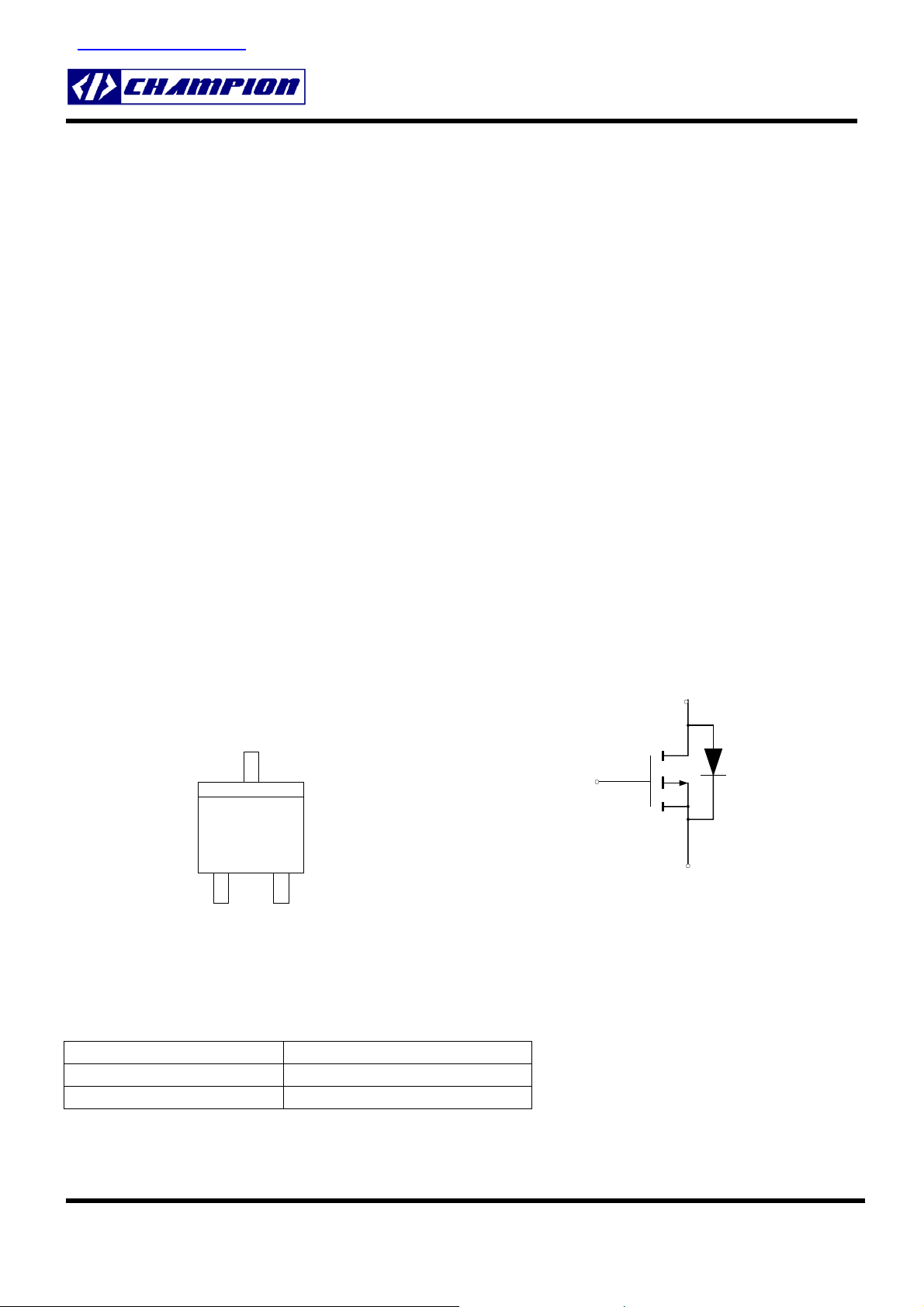
PIN CONFIGURATION
SOT-23-3
Top View
3
CMT2301
HANNEL ENHANCEMENT MODE MOSFET
FEATURES
-20V/-2.3A ,R
-20V/-1.9A ,R
Super high density cell design for extremely low R
Exceptional on-resistance and maximum DC current
capability
SOT-23-3 package design
SYMBOL
=130 m@VGS=-4.5V
DS(ON)
=190 m@VGS=-2.5V
DS(ON)
DS(ON)
D
G
DRAIN
GATE
1
SOURCE
2
P-Channel MOSFET
ORDERING INFORMATION
Part Number Package
CMT2301M233 SOT-23-3
CMT2301GM233* SOT-23-3
*Note: G : Suffix for Pb Free Product
S
2005/01/05 Champion Microelectronic Corporation Page 1
Page 2
CMT2301
HANNEL ENHANCEMENT MODE MOSFET
P-C
ABSOLUTE MAXIMUM RATINGS
Rating Symbol Value Unit
Drain- to- Source Voltage V
Gate-to-Source Voltage V
Continuous Drain Current(TJ=150℃)
TA=25℃ -2.5
T
=70℃
A
Pulsed Drain Current I
Continuous Source Current(Diode Conduction) I
Power Dissipation
TA=25℃ 1.25
T
=70℃
A
Operating Junction Temperature T
Storage Temperature Range T
Thermal Resistance-Junction to Ambient R
DSS
GSS
I
DM
P
STG
D
S
D
J
JA
ELECTRICAL CHARACTERISTICS
Unless otherwise specified, TJ = 25℃.
CMT2301
Characteristic Symbol Min Typ Max Units
Static
Drain-Source Breakdown Voltage
= 0 V, ID = -250μA)
(V
GS
Gate Threshold Voltage
= VGS, ID = -250μA)
(V
DS
V
(BR)DSS
V
Gate Leakage Current
=0 V, VGS = ±8 V)
(V
DS
Zero Gate Voltage Drain Current
= -20 V, VGS = 0 V)
(V
DS
= -20 V, VGS = 0 V, TJ = 55℃)
(V
DS
On-State Drain Current
(V
(V
≤ -5 V, V
DS
≤ -5 V, V
DS
= -4.5V)
GS
= -2.5V)
GS
I
Drain-Source On-Resistance
= -4.5 V, ID = -2.8A)
(V
GS
= -2.5 V, ID = -2.0A)
(V
GS
R
Forward Transconductance (VDS = -5 V, ID = -2.8V) g
Diode Forward Voltage (IS=-1.6A,VGS=0V) V
Dynamic
Input Capacitance C
Output Capacitance C
Reverse Transfer Capacitance
Turn-On Time
Turn-Off Time
Total Gate Charge Q
Gate-Source Charge Q
Gate-Drain Charge
(V
= -6 V, VGS =-0V,
DS
f = 1.0 MHz)
(V
= -6 V,RL=6
DD
= -1.0 A,V
I
D
= 6)
R
G
(V
= -6 V, ID = -2.8 A,
DS
=-4.5V)
V
GS
= -4.5 V,
GEN
t
t
GS(th)
I
GSS
I
DSS
D(on)
DS(on)
FS
SD
iss
oss
C
rss
d(on)
tr 36 60
d(off)
tf 34 60
g
gs
Q
gd
-20
-0.45 -1.5
±100
-6
-3
6.5 S
-0.8 -1.2 V
415
223
87
13 25
42 70
5.8 10
0.85
1.7
-20 V
±8 V
-1.5
-10 A
-1.6 A
0.8
150 ℃
-55/150 ℃
120 ℃/W
-1
-10
0.105
0.145
0.13
0.19
A
W
V
V
nA
μA
A
pF
ns
nC
2005/01/05 Champion Microelectronic Corporation Page 2
Page 3

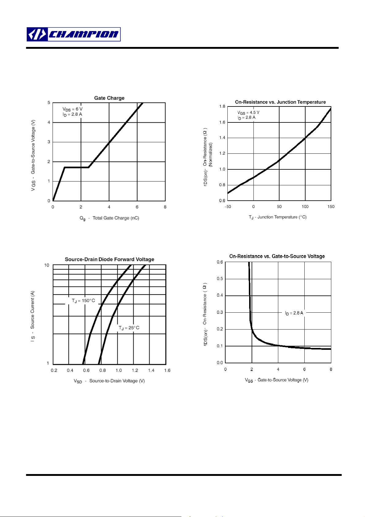
TYPICAL CHARACTERISTICS
CMT2301
HANNEL ENHANCEMENT MODE MOSFET
P-C
2005/01/05 Champion Microelectronic Corporation Page 3
Page 4
TYPICAL CHARACTERISTICS
CMT2301
HANNEL ENHANCEMENT MODE MOSFET
P-C
2005/01/05 Champion Microelectronic Corporation Page 4
Page 5

TYPICAL CHARACTERISTICS
CMT2301
HANNEL ENHANCEMENT MODE MOSFET
P-C
2005/01/05 Champion Microelectronic Corporation Page 5
Page 6

PACKAGE DIMENSION
D
CMT2301
HANNEL ENHANCEMENT MODE MOSFET
P-C
SOT-23-3
3
E
E1
12
e
e1
θ
1
θ
2
c
Base Metal
b
A2
A
A1
See Section B-B
b1
b
Section B-B
c1
With Plating
A
A1
A2
b
b1
c
c1
D
E
E1
L
L1
e
e1
θ
θ1
θ2
θ
L
L1
2005/01/05 Champion Microelectronic Corporation Page 6
Page 7
CMT2301
HANNEL ENHANCEMENT MODE MOSFET
P-C
IMPORTANT NOTICE
Champion Microelectronic Corporation (CMC) reserves the right to make changes to its products or to discontinue any
integrated circuit product or service without notice, and advises its customers to obtain the latest version of relevant information
to verify, before placing orders, that the information being relied on is current.
A few applications using integrated circuit products may involve potential risks of death, personal injury, or severe property or
environmental damage. CMC integrated circuit products are not designed, intended, authorized, or warranted to be suitable for
use in life-support applications, devices or systems or other critical applications. Use of CMC products in such applications is
understood to be fully at the risk of the customer. In order to minimize risks associated with the customer’s applications, the
customer should provide adequate design and operating safeguards.
HsinChu Headquarter
5F, No. 11, Park Avenue II,
Science-Based Industrial Park,
HsinChu City, Taiwan
T EL : +886-3-567 9979 T EL : +886-2-8692 1591
FA X : +886-3-567 9909 F A X: +886-2-8692 1596
Sales & Marketing
11F, No. 306-3, SEC. 1, Ta Tung Road,
Hsichih, Taipei Hsien 221, Taiwan
2005/01/05 Champion Microelectronic Corporation Page 7
 Loading...