

Page 1
查询CM339供应商
Page 2
L
OW POWER QUAD VOLTAGE COMPARATORS
GENERAL DESCRIPTION
This device consists of four independent precision voltage
comparators with an offset voltage specification as low as 2mV
max for CM339. All these comparators were designed
specifically to operate from a single power supply over a wide
range of voltages. Operation from split power supplies is also
possible. These Comparators also have a unique
characteristic in that the input common mode voltage range
includes ground even though operated from a single power
supply voltage.
SYMBOL
CM339
FEATURES
! Wide single supply voltage range or dual supplies for all
devices: +2V to +36V or ± 1V to ± 18V
! Very low supply current(1.1mA)independent of supply
voltage(1.4mW/comparator +5V)
! Low input bias current: 25nA typ
! Low input offset current: ±5nA typ
! Low input offset voltage: ±1mV typ
! Input common-mode voltage range inc lud es grou nd
! Low output saturation voltage : 250mV typ,(Io = 4mA)
! Differential input voltage range equal to the supply
voltage
! TTL, DTL, ECL, MOS, CMOS compatible output
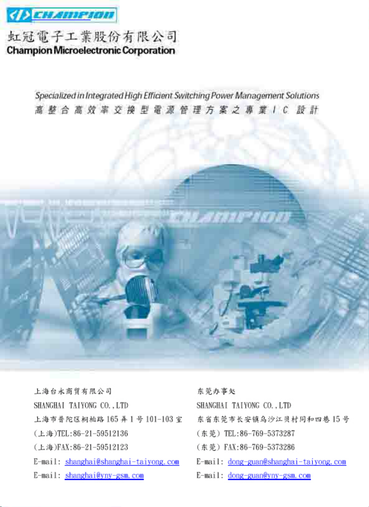
PIN CONFIGURATION
14 Pin PDIP/SOP
(Top View)
1
2
3
4
5
6
7
1OUT
2OUT
VCC
2IN2IN+
1IN-
1IN+
3OUT
4OUT
GND
4IN+
4IN-
3IN+
3IN-
14
13
12
11
10
9
8
2001/07/02
Preliminary
Champion Microelectronic Corporation Page 1
Page 3
CM339
L
OW POWER QUAD VOLTAGE COMPARATORS
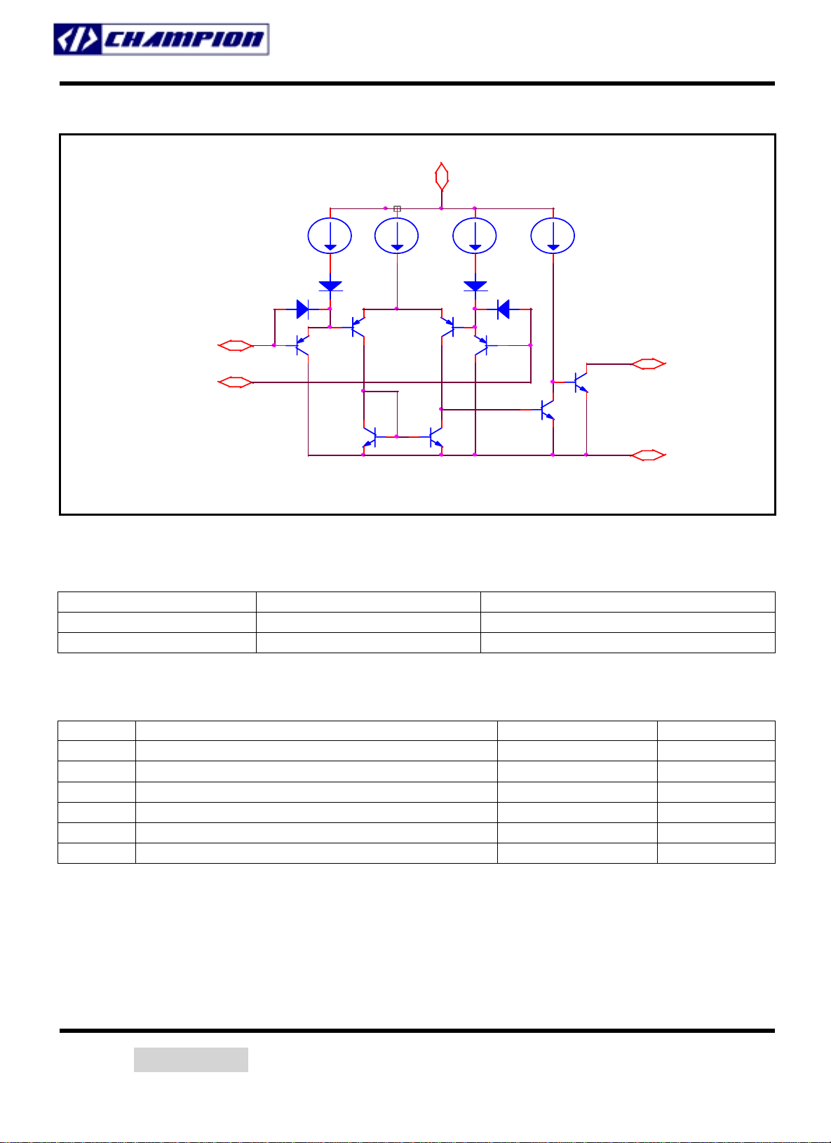
BLOCK DIAGRAM
Non-inv erting Input
Inv erting Input
ORDERING INFORMATION
Part Number Temperature Range Package
CM339CP 0℃ to 70℃ 14-Pin PDIP(P14)
CM339CS 0℃ to 70℃ 14-Pin SOP(S14)
ABSOULTE MAXIMUM RATINGS
Symbol Parameter CM339 Unit
Vcc Supply voltage ±18 to 36 V
Vid Differential input voltage ±36 V
VI Input voltage -0.3 to + 36 V
P
Power dissipation 570 mW
tot
T
Operating free-air temperature range 0, +70 ℃
oper
T
Storage temperature range -65, +150 ℃
stg
Vcc+
3.5uA 100uA100uA3.5uA
Vo
Vcc-
2001/07/02
Preliminary
Champion Microelectronic Corporation Page 2
Page 4

ELECTRICAL CHARACTERISTICS
Vcc+ = +5V, Vcc+ = GND, T
=25℃(Unless otherwise specified)
amb
CM339
L
OW POWER QUAD VOLTAGE COMPARATORS
Symbol Parameter
CM339
Units
Min. Typ. Max.
Vio
Input offset voltage-(note 1)
T
= +25℃
amb
≤ T
≤ T
T
min
amb
max
Iio Input offset current
T
= +25℃
amb
≤ T
T
min
amb
≤ T
max
Iio Input bias current
T
= +25℃
amb
≤ T
amb
≤ T
max
T
min
Avd Large signal voltage gain
Icc
(Vcc = 15, R
Supply current(all comparators)
= 15kΩ, Vo = 1 to 11V)
L
1.0 2.2 MV
5.0 50 nA
25 250 nA
50 200 V/mV
0.8 2.0 mA
Vcc = +5V, no load
Vcc = +30V , no load
V
icm
Input common mode voltage range-(note 2)
0 Vcc
+
- 1.5 V
(Vcc = 30V)
T
= +25℃
amb
T
Vid
I
Output sink current
sink
tre
t
Large signal response time
rel
min
Differential input voltage -(note 4)
(V
= -1V, Vo = 1.5V)
id
Response Time -(note 3)
(R
(R
V
= 5.1kΩ connected to Vcc
L
= 5.1kΩ connected to Vcc+, ei = TTL,
L
(ref)
≤ T
≤ T
amb
)
= +1.4V)
max
36 V
6.0 16 mA
+
1.3
)
μs
300 ns
Notes : 1.At output switch point, Vo = 1.4V, Rs = 0 with Vcc
+
from 5V to 30V, and over the full input common-mode range(0V
to Vcc+ -1.5V).
2.The input common-mode voltage of the either input signal voltage should not be allowed to go negative by more than
+
0.3V. The upper and of the common-mode voltage range is Vcc
-1.5V, but either or both inputs can go to +30V
without damage.
3.The response time specified is for a 100mV input step with 5mV overdrive. For larger overdrive signals 300ns can be
obtained.
4.Positive excursions of input voltage may power supply level. As long as the other voltage remains within the
common-mode range, the comparator will provide a proper output state. The low input voltage state
must not be less than –0.3V(or 0.3V bellow the negative power supply, if used).
200
1/07/02
Preliminary
Champion Microelectronic Corporation Page 3
Page 5

TYPICAL CHARACTERISTICS
Supply Current
CM339
OW POWER QUAD VOLTAGE COMPARATORS
L
Input Current
Output Saturation Voltage
Response Time for Various Input Overdrives – Positive
Transistors
Response Time for Various Input Overdrives – Negative
Transistors
2001/07/02
Preliminary
Champion Microelectronic Corporation Page 4
Page 6

PACKAGE DIMENSION
PIN 1 ID
OW POWER QUAD VOLTAGE COMPARATORS
L
14-PIN PDIP (P14)
θ
CM339
θ
14-PIN SOP (S14)
PIN 1 ID
θ
2001/07/02
Preliminary
θ
Champion Microelectronic Corporation Page 5
Page 7

CERAMIC/SURGE
ABSORBER
SHANGHAI,CHINA
DIODES LAB
HANGZHOU,CHINA
CERAMIC/PZT
SHINCHU,TAIWAN
DC POWER LAB
TAIPEI,TAIWAN
 Loading...