

Page 1

查询CM2831供应商
Page 2
CM2831
GENERAL DESCRIPTION
The CM2831 family is a positive voltage linear regulator
developed utilizing CMOS technology featured low quiescent
current (30µA typ.), low dropout voltage, and high output
voltage accuracy, making them ideal for battery applications.
EN input connected to CMOS has low bias current. The
space-saving SOT-23-5 package is attractive for “Pocket” and
“Hand Held” applications.
These rugged devices have both Thermal Shutdown, and
Current Fold-back to prevent device failure under the “Worst”
of operating conditions.
In application requiring a low noise, regulated supply, place a
1000pF capacitor between Bypass and Ground.
The CM2831 is stable with an output capacitance of 2.2µF or
greater.
APPLICATIONS
! Battery-powered devices
! Personal communication devices
!
Home electric/electronic appliances
! PC peripherals
300mA CMOS LDO W
FEATURES
! Very Low Dropout Voltage
!
Low Current Consumption: Typ. 30µA, Max. 35µA
! Output Voltage: 1.5V, 1.8V, 1.9V, 2.2V, 2.5V, 2.7V, 2.8V,
2.9V, 3.0V, 3.3V, 3.5V, 3.6V, and 3.8V
! High Accuracy Output Voltage: +/- 1.5%
! Guaranteed 300mA Output
! Input Range of 2.6V to 7.0V
! Thermal Shutdown
! Curre nt Limiting
! Compact Package: SOT-23-5
!
Factory Pre-set Output Voltages
! Short Circuit Current Fold-Back
! Low Temperature Coefficient
24 Hours Technical Support--WebSIM
Champion provides customers an online circuit simulation tool
called WebSIM. You could simply logon our website at
www.champion-micro.com for details.
ITH
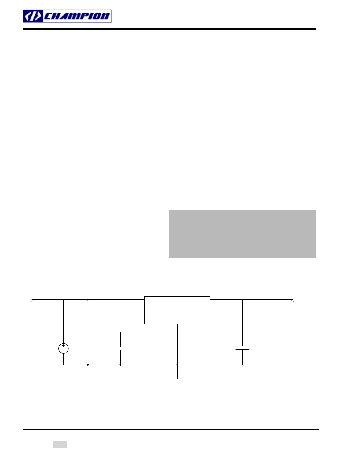
TYPICAL APPLICATIONS
IN OUT
IN O UT
CM2831
BYP GND EN
E
NABLE
5V
2002/04/12
C1
1uF
Rev. 3
Champion Microelectronic Corporation Page 1
C2
1nF
C3
2.2uF
Page 3
CM2831
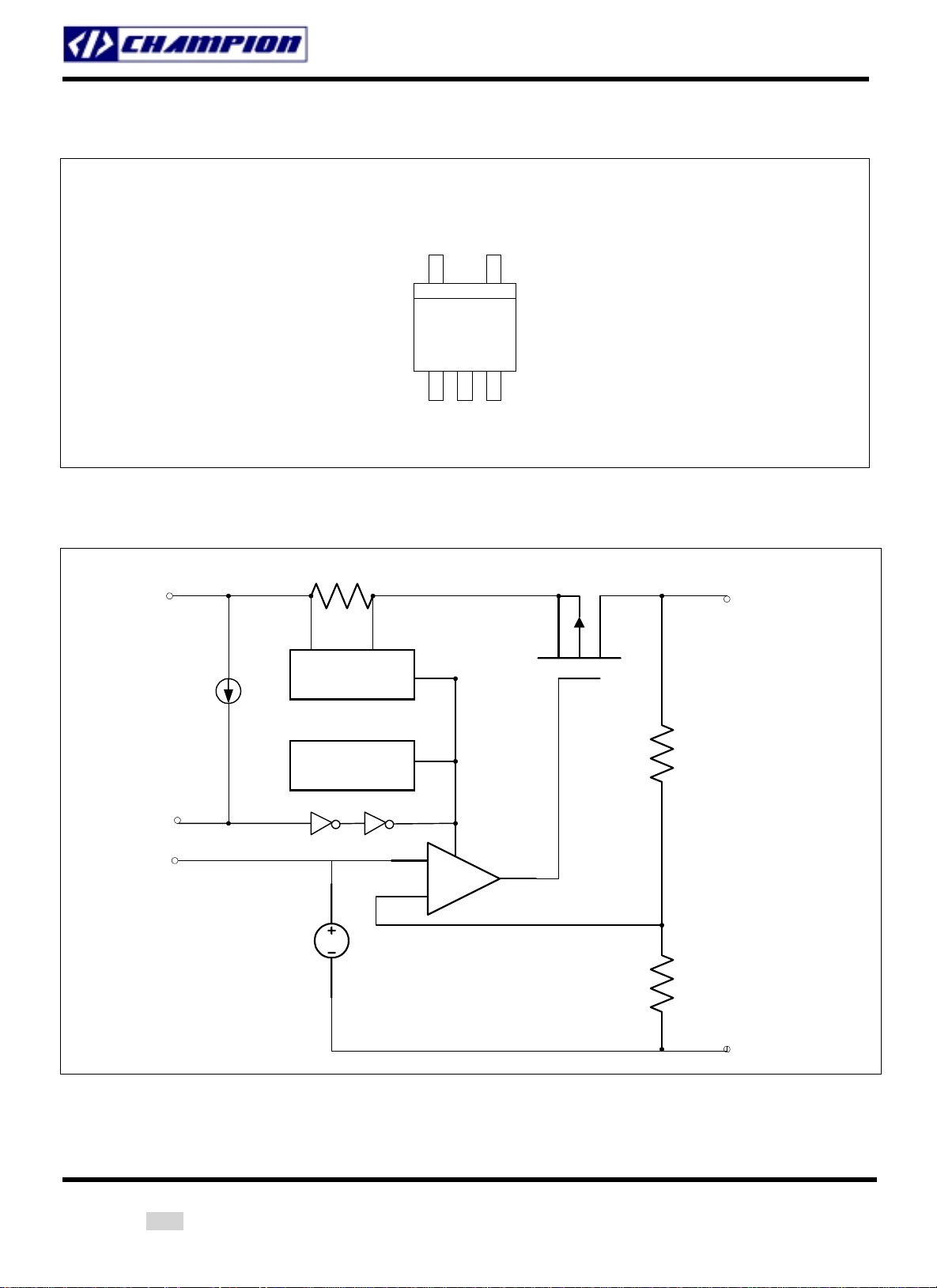
PIN CONFIGURATION
BLOCK DIAGRAM
300mA CMOS LDO W
SOT-23-5
Top View
5
VIN VOUT
1
2
4
GND
3
BYP
EN
ITH
E
NABLE
IN
OUT
Overcurrent
1uA
Shutdown
Thermal
R1
Shutdown
EN
BYP
-
AMP
+
Vref = 1.176V
R2
GND
2002/04/12
Rev. 3
Champion Microelectronic Corporation Page 2
Page 4
CM2831
300mA CMOS LDO W
ITH
E
NABLE
ORDERING INFORMATION
Part Number Output Voltage Temperature Range Package
CM2831AIM25 1.5V -40℃ ~ +85℃ SOT-23-5
CM2831DIM25 1.8V -40℃ ~ +85℃ SOT-23-5
CM2831EIM25 1.9V -40℃ ~ +85℃ SOT-23-5
CM2831HIM25 2.2V -40℃ ~ +85℃ SOT-23-5
CM2831KIM25 2.5V -40℃ ~ +85℃ SOT-23-5
CM2831MIM25 2.7V -40℃ ~ +85℃ SOT-23-5
CM2831NIM25 2.8V -40℃ ~ +85℃ SOT-23-5
CM2831OIM25 2.9V -40℃ ~ +85℃ SOT-23-5
CM2831PIM25
CM2831SIM25
CM2831UIM25
CM2831VIM25
CM2831XIM25
Note: For other pre-set output voltage requirements, please contact Champion Sales office.
ABSOLUTE MAXIMUM RATINGS
3.0V
3.3V
3.5V
3.6V
3.8V
-40℃ ~ +85℃ SOT-23-5
-40℃ ~ +85℃ SOT-23-5
-40℃ ~ +85℃ SOT-23-5
-40℃ ~ +85℃ SOT-23-5
-40℃ ~ +85℃ SOT-23-5
OPERATING RATINGS
Input Voltage …………….……………………………. +7V
Output Current …………………….…… P
Output Voltage …………………… GND-0.3V to VIN+0.3V
ESD Classification ………………………………………… B
/ (VIN - Vo) mA
D
Ambient Temperature Range (T
Junction Temperature Range …..…... -40℃ to +125℃
) ……... -40℃ to +85℃
A
THERMAL INFORMATION
Parameter Maximum Unit
Thermal Resistance (Θjc)
Internal Power Dissipation (PD)
(ΔT = 100℃)
Maximum Junction Temperature 150
Maximum Lead Temperature (10 Sec) 300
Caution: Stress above the listed absolute rating may cause permanent damage to the device.
SOT-23-5 260
SOT-23-5 380
℃/W
℃/W
℃
℃
2002/04/12
Rev. 3
Champion Microelectronic Corporation Page 3
Page 5

CM2831
300mA CMOS LDO W
ITH
ELECTRICAL CHARACTERISTICS
= +25℃; unless otherwise noted
T
A
Parameter Symbol Test Conditions
Min. Typ. Max.
Input Voltage VIN Note 1 7 V
Output Voltage Accuracy V
Dropout Voltage V
Output Current IO V
Current Limit I
Short Circuit Current ISC V
Quiescent Current IQ I
Ground Pin Current I
Line Regulation REG
Load Regulation REG
I
OUT
IO = 300mA, V
DROPOUT
LIM
GND
IO = 300mA, V
V
I
=5mA, VIN=V
I
OUT
LINE
I
LOAD
= 1mA to 300mA -1.5 1.5 %
O
OUT=VO(NOM)
OUT=VO(NOM)
OUT
OUT
OUT
O
= 1mA to 300mA 30 50 μA
O
OUT
V
+2
OUT
=1mA to 300mA 0.2 1 %
O
-2%, V
> 1.2V 300 mA
> 1.2V 300 450 mA
< 0.95V 150 300 mA
= 0mA 30 35 μA
+1 to
>=2.5V 300
OUT
-2%, V
V
V
<2.5V 800
OUT
<= 3.0V -0.15 0.03 0.15 %
OUT
> 3.0V -0.3 0.06 0.3 %
OUT
Over Temperature Shutdown OTS 150
Over Temperature Hysteresis OTH 30
V
Temperature Coefficient TC 25 ppm/℃
OUT
= 100mA
I
Power Supply Rejection PSRR
Power Supply Rejection PSRR
Output Voltage Noise eN
Output Voltage Noise eN
Shutdown Supply Current ISD V
EN Input Bias Current
EN Input Threshold
Note 1.
V
IN(MIN)
= V
OUT
+ V
DROPOUT
IEH V
IEL V
VEH V
VEL V
O
CO=2.2µF ceramic
I
= 100mA
O
=2.2µF ceramic
C
O
C
BYP
f=10Hz to 100kHz
= 10mA, C
I
O
f=10Hz to 100kHz
= 10mA, C
I
O
=5.0V, V
IN
=0.01µF
=0µF
BYP
=0.01µF
BYP
=0V, VEN < VEL 2.0 3.0 μA
OUT
, VIN=2.6V to 7V 0.1 μA
EN=VIN
, VIN=2.6V to 7V 1.0 3.0 μA
EN=VIN
=2.6V to 7V VIN/2+0.8V VIN V
IN
=2.6V to 7V 0 VIN/2-0.8V V
IN
f=1kHz 60
f=10kHz 50
f=100kHz 40
f=1kHz 75
f=10kHz 55
f=100kHz 30
CO=2.2µF 30
C
=100µF 20
O
CO=2.2µF 30
=100µF 20
C
O
CM2831
E
NABLE
Unit
mV
℃
℃
dB
dB
μVrms
μVrms
2002/04/12
Rev. 3
Champion Microelectronic Corporation Page 4
Page 6

CM2831
300mA CMOS LDO W
ITH
E
NABLE
DETAILED DESCRIPTION
The CM2831 family of CMOS regulators contain a PMOS pass transistor, voltage reference, error amplifier, over-current
protection, thermal shutdown, and short circui t protect ion .
The P-channel pass transistor receives data from the error amplifier, over-current shutdown, short output protection, and thermal
protection circuits. During normal operation, the error amplifier compares the output voltage to a precision reference. Over-current
and Thermal shutdown circuits become active when the junction temperature exceeds 150℃, or the current exceeds 300mA.
During thermal shutdown, the output voltage remains low. Normal operation is restored when the junction temperature drops
below 120℃.
The CM2831 switches from voltage mode to current mode when the load exceeds the rated output current. This prevents
over-stress. The CM2831 also incorporates current fold-back to reduce power dissipation when the output is short-circuited. This
feature becomes active when the output drops below 1.05V, and reduces the current flow by 65%. Full current is restored when
the voltage exceeds 0.95V.
ENABLE
The Enable pin normally floats high. When actively, pulled low, the PMOS pass transistor shut off, and all internal circuits are
powered down. In this state, the quiescent current is less than 2µA. This pin behaves much like an electronic switch.
EXTERNAL CAPACITOR
The CM2831 is stable with an output capacitor to ground of 2.2µF or greater. It can keep stable even with higher or poor ESR
capacitors. A second capacitor is recommended between the input and ground to stabilize VIN. The input capacitor should be
larger than 0.1µF to have a beneficial effect. All capacitors should be placed in close proximity to the pins. A “quiet” ground
termination is desirable.
2002/04/12
Rev. 3
Champion Microelectronic Corporation Page 5
Page 7

CM2831
300mA CMOS LDO W
TYPICAL ELECTRICAL CHARACTERISTICS
ITH
E
NABLE
2002/04/12
Rev. 3
Champion Microelectronic Corporation Page 6
Page 8

CM2831
300mA CMOS LDO W
ITH
E
NABLE
2002/04/12
Rev. 3
Champion Microelectronic Corporation Page 7
Page 9

CM2831
300mA CMOS LDO W
ITH
E
NABLE
2002/04/12
Rev. 3
Champion Microelectronic Corporation Page 8
Page 10

CM2831
PACKAGE DIMENSION
D
300mA CMOS LDO W
SOT-23-5 (M25)
ITH
E
NABLE
5
E
E1
123
e
θ1
θ2
4
c
Base Metal
e1
b
A2
A
A1
See Section B-B
b1
b
Section B-B
c1
With Plating
A
A1
A2
b
b1
c
c1
D
E
E1
L
L1
e
e1
θ
θ1
θ2
θ
L
L1
2002/04/12
Rev. 3
Champion Microelectronic Corporation Page 9
Page 11

CM2831
300mA CMOS LDO W
ITH
E
NABLE
NUMBERING SCHEME
Ordering Number: CM2831XYZ (note1)
note1:
CM2831 : 300mA CMOS LDO with enable
X : Suffix for voltage output (note 2)
: Suffix for Temperature Range (note 3)
Y
: Suffix for Package Type (note 4)
Z
note 2: see CMOS LDO Voltage Suffix Table
CM2831 will provide options of A(1.5V), D (1.8V), E(1.9V),, H(2.2V), K(2.5V), M(2.7V), N(2.8V), O(2.9V), P(3.0V), S(3.3V),
U(3.5V), V(3.6V), X(3.8V)
:
note 3
~+85℃ (only I grade support for all CMOS LDOs)
Y= I : -40
note 4:
Z is single alphabet with or without digits
M25 : SOT-25 (TR only)
℃
CMOS LDO Voltage Suffix Table
Output Voltage Suffix Output Voltage Suffix
1.5V A 3.0V P
1.6V B 3.1V Q
1.7V C 3.2V R
1.8V D 3.3V S
1.9V E 3.4V T
2.0V F 3.5V U
2.1V G 3.6V V
2.2V H 3.7V W
2.3V I 3.8V X
2.4V J 3.9V Y
2.5V K 4.0V Z
2.6V L
2.7V M
2.8V N
2.9V O
2002/04/12
Rev. 3
Champion Microelectronic Corporation Page 10
Page 12

CERAMIC/SURGE
ABSORBER
SHANGHAI,CHINA
DIODES LAB
HANGZHOU,CHINA
CERAMIC/PZT
SHINCHU,TAIWAN
DC POWER LAB
TAIPEI,TAIWAN
 Loading...