

Page 1

Federal Communications Commission Statement
This device complies with FCC Rules Part 155. Operation is subject to the following two
conditions:
w This device may not cause harmful interference
w This device must accept any interference received, including interference that may cause
undesired operation.
This equipment has been tested and found to comply with the limits for a Class B digital device,
pursuant to Part 15 of the FCC Rules. These limits are designed to provide reasonable protection
against harmful interference in a residential installation. This equipment generates, uses and can
radiate radio frequency energy. If this equipment is not installed and used in accordance with the
manufacturer's instructions, it may cause harmful interference to radio communications. However,
there is no guarantee that interference will not occur in a particular installation. If this equipment
does cause harmful interference to radio or television reception, which can be determined by
turning the equipment off and on, the user is encouraged to try to correct the interference by
one or more of the following measures:
w Reorient or relocate the receiving antenna.
w Increase the separation between the equipment and receiver.
w Connect the equipment to an outlet on a circuit different from that to which the receiver
is connected.
w Consult the dealer or an experienced radio/TV technician for help.
The use of shielded cables for connection of the monitor to the graphics card is required to
assure compliance with FCC regulations. Changes or modifications to this unit not expressly
approved by the party responsible for compliance could void the user's authority to operate this
equipment.
Canadian Department of Communications Statement
This digital apparatus does not exceed the Class B limits for audio noise emissions from digital
apparatusses set out in the Radio Interference Regulations of the Canadian Department of
Communications.
Manufacturer's Disclaimer Statement
The information in this document is subject to change without notice and does not represent a
commitment on the part of the vendor. No warranty or representation, either expressed or implied, is
made with respect to the quality, accuracy or fitness for any particular purpose of this document. The
manufacturer reserves the right to make changes to the content of this document and/or the products
associated with it at any time without obligation to notify any person or organization of such changes.
In no event will the manufacturer be liable for direct, indirect, special, incidental or consequential
damages arising out of the use or inability to use this product or documentation, even if advised of the
possibility of such damages. This document contains materials protected by copyright. All rights are
reserved. No part of this manual may be reproduced or transmitted in any form, by any means or for
any purpose without expressed written consent of it's authors. Product names appearing in this
document are mentioned for identification purposes only. All trademarks, product names or brand
names appearing in this document are registered property of their respective owners.
Printed in Taiwan
March 1998March 1998
March 1998
March 1998March 1998
POST-CONSUMER
RECYCLED PAPER
i
Page 2

Table of Contents
Chapter 1 Introduction.................................................................1
1-1 Product Specifications .......................................................... 1
1-2 Package Contents.................................................................3
1-3 Mainboard Layout ..................................................................4
1-4 Jumper and Connector Reference Page Chart ...................... 4
Chapter 2 Hardware Setup..............................................................5
2-1 Introduction to Jumpers .........................................................5
2-2 Installing a PGA type CPU in a ZIF Socket ..........................6
2-3 CPU Jumper Configuration ....................................................7
2-4 Connector and Jumper Settings.......................................... 10
2-5 Main Memory Configuration ................................................16
Chapter 3 Award BIOS Setup Program .......................................... 19
3-1 Standard CMOS Setup ........................................................20
3-2 BIOS Features Setup ..........................................................23
3-3 Chipset Features Setup ......................................................26
3-4 Power Management Setup ..................................................28
3-5 PnP/PCI Configuration.........................................................32
3-6 Load Setup Defaults ............................................................34
3-7 Integrated Peripherals..........................................................35
3-8 Supervisor Password & User Password Setting ................37
3-9 IDE HDD Auto Detection .....................................................39
3-10 Save and Exit Setup............................................................39
3-11 Exit Without Saving.............................................................39
Chapter 4 Mainboard Software Guide ...........................................41
- VIA ACPI Patch for Win 95
- VIA IDE Bus Master Drivers for Win95 and WinNT
- VIA AGP VxD Drivers for Win 95
- Trend Antivirus Utility for Win95
- Shepherd System Monitoring Software for Win95 OR
Genesys System Monitoring Software for Win95/WinNT
- Award Flash Utility
- Award DMI Configuration Utility
ii
Page 3

Feature ExplanationsFeature Explanations
Feature Explanations
Feature ExplanationsFeature Explanations
Software Power-Off Control...........................................................11
Power-On By Modem.............................................................. 11/32
Over-ride Power Button Connector ................................................ 12
Poly-fuse Over Current Protection ................................................. 14
Flash BIOS Protection................................................................... 27
Power-On By Alarm....................................................................... 32
Quick Connector and Jumper Reference ..................................... 22-A
Appendix I On Board I/O Addresses & IRQ Maps............................ 43
Appendix II FAN78-
Reader's Feedback ............................................................................ 47
SMART
Technology Upgrade Kit .................... 45
iii
Page 4

- Memo
iv
Page 5

Introduction
Chapter 1
Introduction
1-1 Product Specifications
rr
r CPU
rr
- Supports up to 200MHz Intel Pentium® processors and up to 233MHz
Pentium® processors with MMXTM technology
- Supports Intel Pentium® P54CTB OverDrive processors
- Supports PR120+ ~ PR200+ Cyrix/IBM 6x86
later)/6x86L
- Supports PR75 ~ PR166 AMD-K5TM processors and up to 266 MHz K6
processors
- Supports 180 ~ 200MHz IDT WinChip C6 processors
- Supports 60/66 MHz system clock speeds
- 321-pin ZIF Socket 7
- High efficiency Switching Power Module
Supports 68/75MHz system clock for over-clocking possibility
r Cache Memory
- Standard 512KB (64k*64x1) Pipelined Burst SRAM on board
r Main Memory
- Two 5V 72-Pin SIMM sockets support 4/8/16/32MB, 32/36-bit, DRAM
memory modules
- Two 3.3V unbuffered 168-pin DIMM sockets support 8/16/32/64/128MB,
64/72-bit DRAM memory modules
- Supports Synchronous(12ns or faster)/EDO/FPM(70ns or faster) DRAM
modules
- Maximum 256MB memory size
r Chipset
- VIA VP3 (82C597AT/82C586B) two chip PCIset
rr
r I/O Slots
rr
- Three 16-bit ISA slots
- Three 32-bit PCI slots (all are Master Mode, PCI 2.1 compliant)
- One 124-pin AGP slot (Accelerated Graphics Port v1.0 compliant)
TM
processors and PR166+ ~ PR233+ 6x86MXTM processors
TM
(processor rev. 2.7 or
TM
1
Page 6

Chapter 1
r Boot Block Flash BIOS
- Award System BIOS supports PnP, APM, DMI & multi-device booting such
as HDD (IDE, SCSI), CD-ROM, LS120, ZIP-ATAPI
- Includes Trend ChipAway Virus for a virus-free system boot-up
rr
r On Board Ultra I/O Functions
rr
- ITE 8661 I/O chip
- One floppy disk drive connector supports up to 2.88MB, Japanese 3 Mode,
and 1Mbps transfer rates
- Two 16550A compliant serial ports
- One Standard/ECP/EPP parallel port
- Supports up to 115.2kbps IrDA IR function
rr
r Two Ultra DMA-33 PCI IDE Ports
rr
- Supports up to PIO Mode 4, Multi-word DMA Mode 2 & Ultra DMA-33
timings
- Complete Bus Master Drivers for well-known multi-tasking operating
systems
rr
r Two Channel USB Ports
rr
Under compatibility testing with different peripherals
r PCB Dimension
- Baby-AT form factor, 220mm x 230mm, 4-layer PCB
- Five mounting holes
rr
r Green PC
rr
- Meets EPA Green PC standard: power consumption under 30W in Doze,
Standby or Suspend modes
rr
r Advanced Management Capability
rr
- Supports Software power off control, Over-ride power button, Power-on by
modem, Power-on by alarm, etc.
- Poly-fuse over-current protection for USB and keyboard
- Flash BIOS protection
2
Page 7
Introduction
1-2 Package Contents
This product comes with the following components:
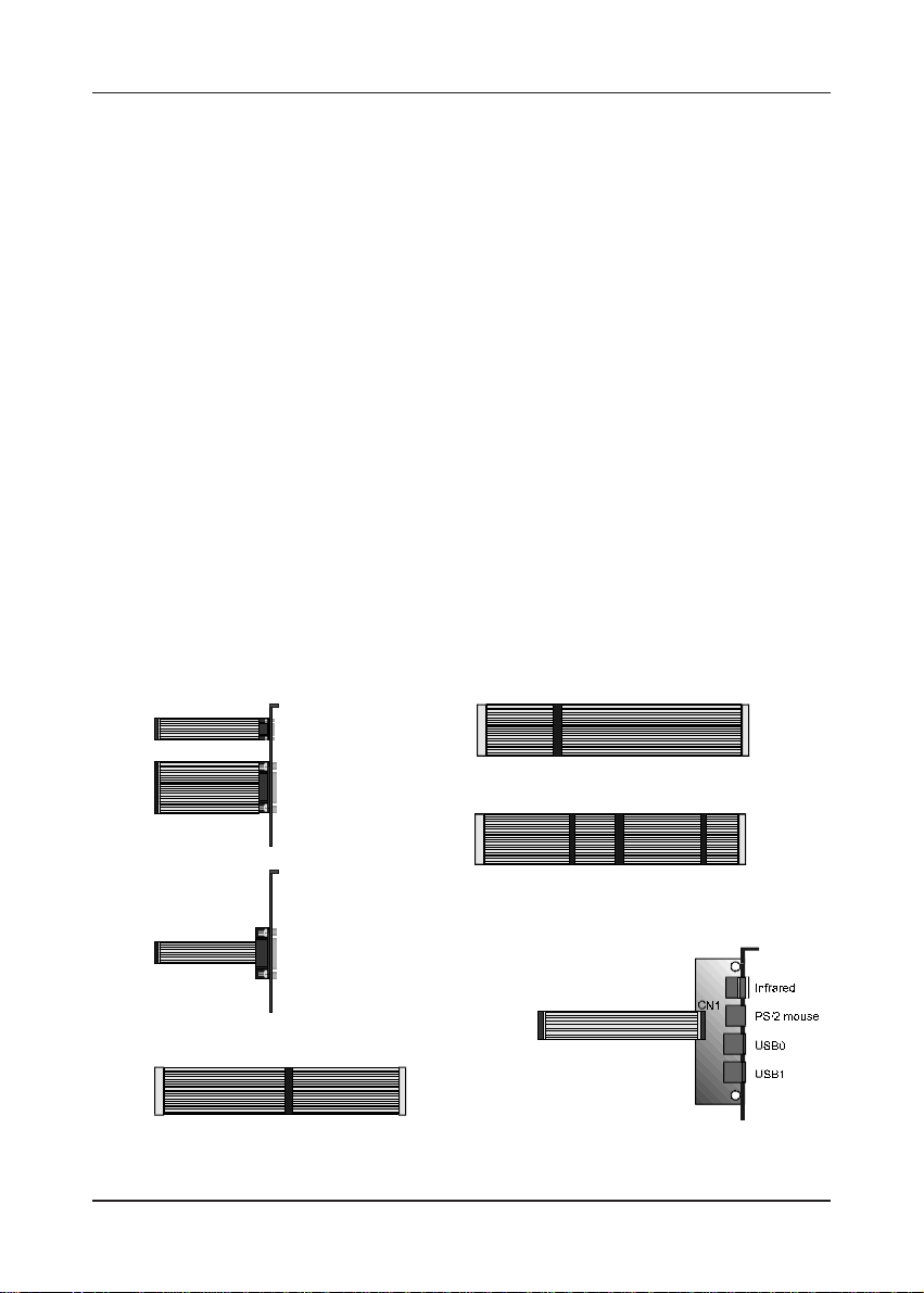
r One mainboard
r One 9-pin serial port and 25-pin parallel port ribbon cable with bracket
(Figure 1-1)
r One 25-pin serial port ribbon cable with bracket (Figure 1-2)
r One 40-pin IDE connector ribbon cable (Figure 1-3)
r One 34-pin floppy disk drive ribbon cable (Figure 1-4a) or (Figure 1-4b)
r Optional USB kit with PS/2 mouse, infrared and two USB ports (Figure 1-5)
r One CD-ROM disk that includes
- Award Flash EPROM Utility, Award DMI Utility
- VIA IDE Bus Master Drivers for Win95 and WinNT
- VIA ACPI Patch
- VIA AGP VxD Drivers for Win95
- Shepherd System Monitoring Software for Win95 OR Genesys System
Monitoring Software for Win95/WinNT
- Trend PC-cillin Anti-virus v3.0 (OEM) Utility for Win95 in eight different
languages
r One User's Manual
Figure 1-1
Figure 1-2
Figure 1-3
Serial port
Parallel port
Serial port
IDE cable
Figure 1-4a
Figure 1-5 optional USB Kit
Standard floppy cable
Optional 5.25 in. floppy cableFigure 1-4b
3
Page 8
Chapter 1
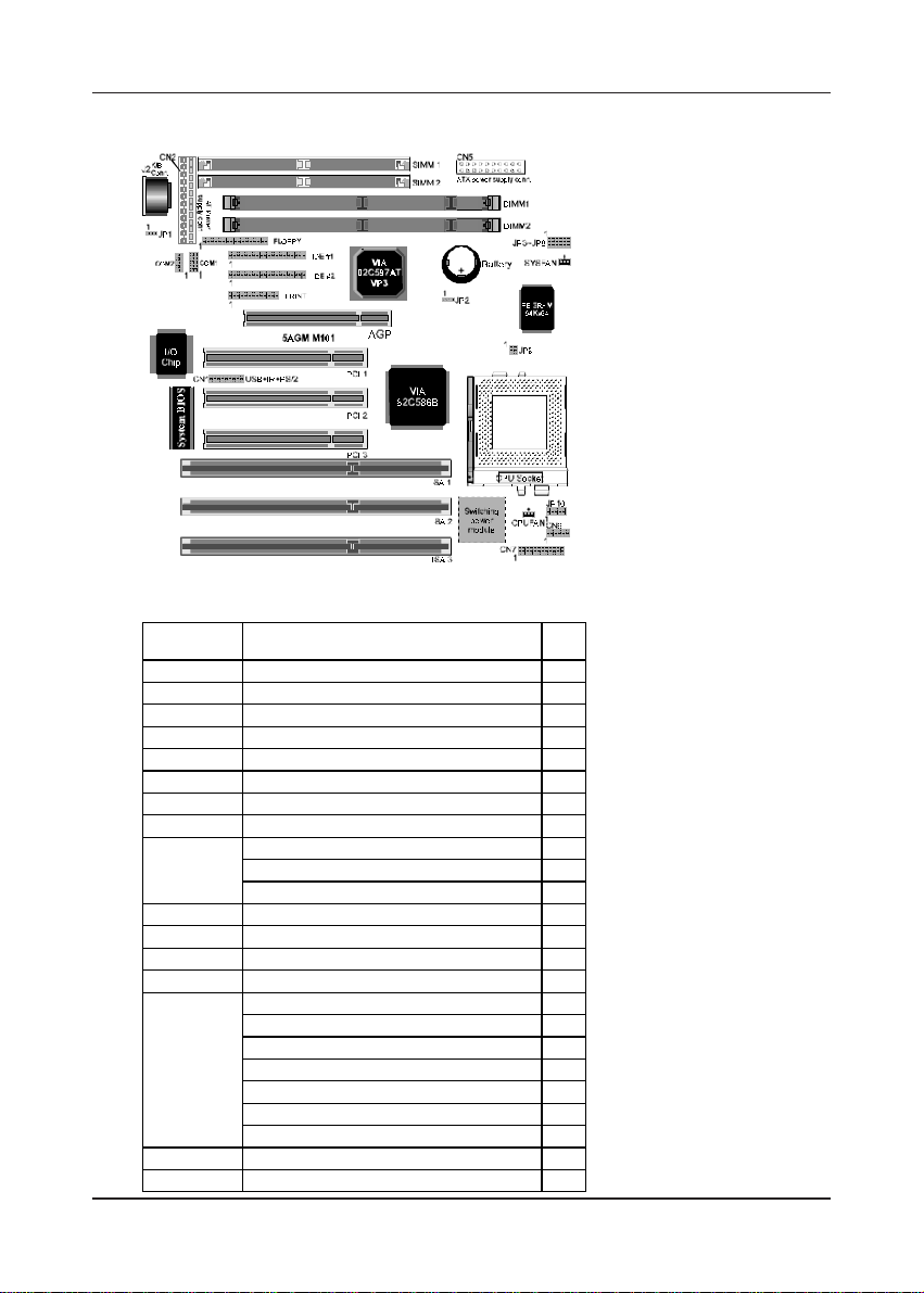
1-3 Mainboard Layout
1-4 Jumper and Connector Reference Page Chart
4
Jumper &
Connector No.
J2 Keyboard connector 14
JP1 AT/ATX power supply jumper 10
JP2 Clear CMOS data jumper 11
JP3-5 System frequency jumpers 7/9
JP6-8 System frequency ratio jumpers 7/9
JP9 Reserved for factory --
JP10 CPU voltage jumpers 8/9
CN1 PS/2 mouse, USB, Infrared connector 14
PS/2 mouse connector 15
USB connector 15
Infrared connector 14
CN2 AT Power supply connector 10
CN5 ATX Power supply connector 10
CN6 FAN-78 connector 45
CN7 Front panel connector set 12/13
Keyboard lock & Power indicator LED connector 12
System reset switch connector 13
Speaker connector 13
Green switch & Green LED connector 13
Turbo LED connector 13
IDE activity LED connector 13
Override power button (for ATX power supply) 12
SYSFAN System cooling fan connector 11
CPUFAN CPU cooling fan connector 11
Function Page
Page 9
Hardware Setup
Chapter 2
Hardware Setup
If your mainboard has already been installed in your computer you may still need
to refer to this chapter if you plan to upgrade your system's hardware.
Be sure to disconnect the power cable from the power source before
performing any work on your mainboard, i. e. installing a CPU, memory
module, changing a jumper setting, adding or removing expansion cards
etc. Not doing so may result in electrical shock or severe damage to your
mainboard and peripherals!
2-1 Introduction to Jumpers
Jumpers are used to select between various operating modes. A jumper consists
of a row of gold colored pins that protrude from the surface of the mainboard. It
is important not to confuse jumpers with connectors or headers.
Putting jumper caps on anything that is not a jumper may result in
damaging your mainboard. Please refer to Section 1-3, Mainboard
Layout, for the location of jumpers on your mainboard.
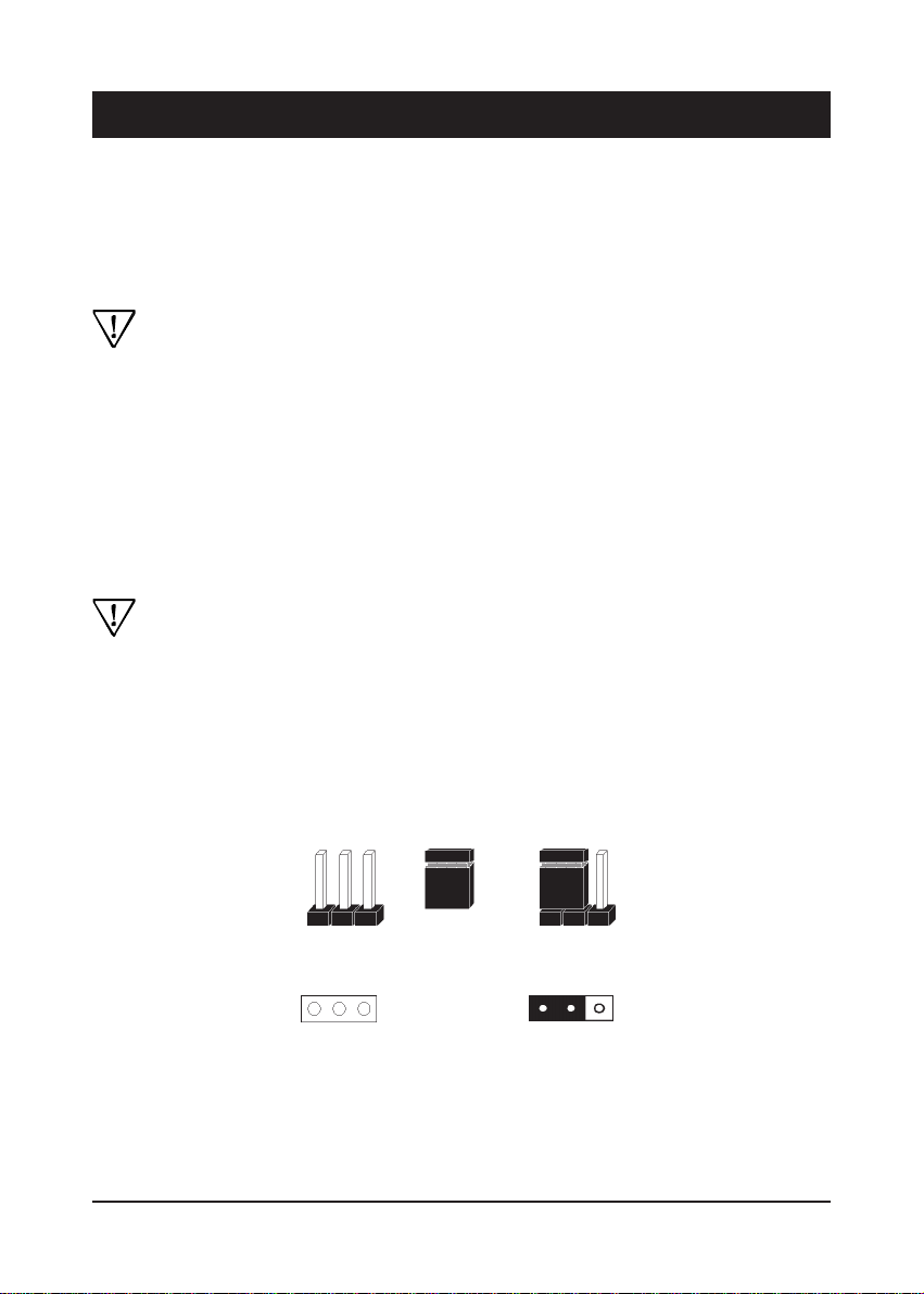
As indicated in Figure 2-1 below, a cap is used to cover the pins of a jumper, resulting
in shorting those pins that it covers. If the cap is removed from the top of the pins,
the jumper is left "open." The number 1 shown both in the diagram below and in
all multiple pin jumper and header diagrams in this manual indicates the pin designated
with the number 1. The numbering of the remaining pins follows in sequence.
Pins SettingCap
1
A 3-pin jumper
Figure 2-1
1
A cap over pin 1 and
pin 2 short these pins
5
Page 10
Chapter 2
2-2 Installing a PGA type CPU in a ZIF Socket
The Intel Socket 7, designed for the Pentium processor, has been incorporated as
a standard mainboard specification and is compatible with AMD and Cyrix CPUs.
To insert your CPU into Socket 7 please do the following:
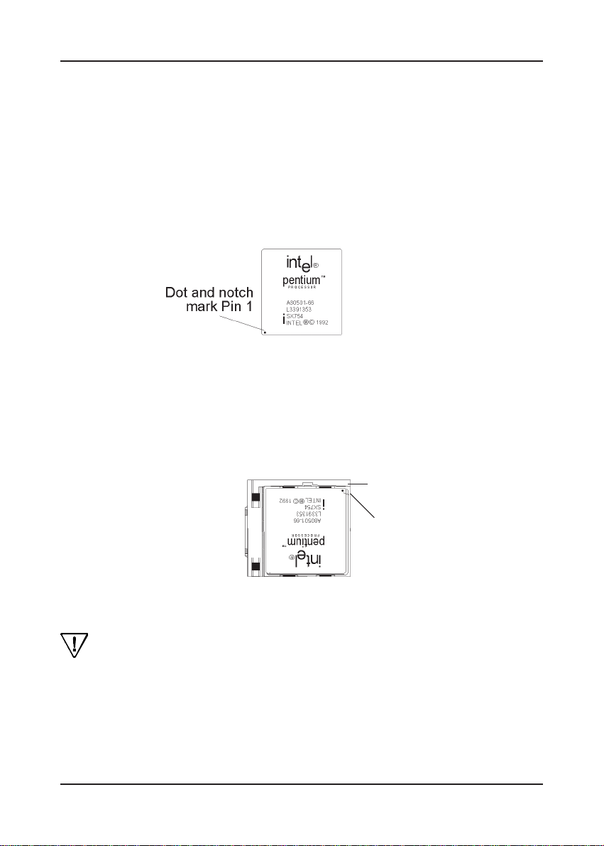
1. Locate a small dot marked on the top surface of the CPU close to one if it's corners.
The same corner will also be cut off, leaving a noticeable notch in the CPU's corner.
These markings indicate Pin 1 of the CPU. See Figure 2-2.
Figure 2-2 The markings on top of a CPU
2. Pull up the lever of Socket 7 so that it is perpendicular with the surface of the
mainboard. Gently insert the CPU with Pin 1 at the same corner of Socket 7 that
contains the end of the lever. Allow the the weight of the CPU to push itself
into place. Do not apply extra pressure as doing so may result in damaging your
CPU. Snap the lever back into place. See Figure 2-3.
Lever
Socket 7
Pin 1
Figure 2-3 Inserting a CPU into Socket 7
Installing a heat sink and cooling fan on top of your CPU is necessary for
proper heat dissipation. Failing to install these items may result in overheating
and possible burn-out of your CPU.
6
Page 11
Hardware Setup
JP6~JP8
2-3 CPU Jumper Configuration
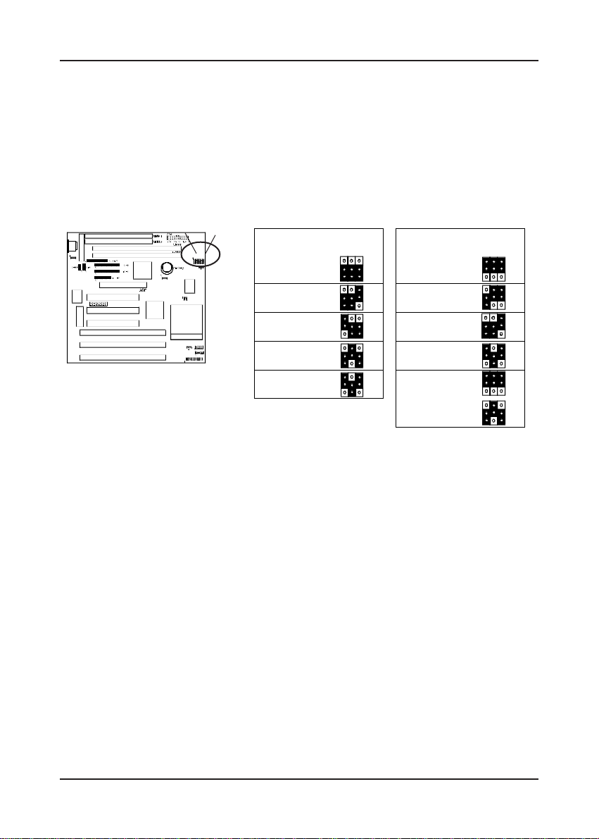
Frequency Configuration
If you install a CPU on this mainboard, you must set JP 3-5 for System Frequency
and JP 6-8 for CPU Bus Frequency Ratio. See Figure 2-4 CPU/System Frequency
Jumper Settings.
CPU Bus Frequency & Frequency Ratio Configuration
JP3~JP5 JP6~JP8
System Freq. JP3~JP5
50MHz
55MHz
60MHz
66MHz
75MHz
Figure 2-4 System Frequency Jumper Settings
1
1
1
1
1
Freq. Ratio
x 1.5
x 2
x 2.5
x 3
x 3.5
x 4
1
1
1
1
1
1
* CPU Speed = Frequency ratio x System Frequency
Overclocking
Operating a CPU at a higher frequency than its specification allows is called
overclocking. If the CPU frequency is set at a higher frequency than its specification
allows, it may or may not run at that freqency, depending on the quality of the CPU
and the extent to which the the frequency has been overset. The mainboard manufacturer
highly discourages overclocking as it may result in data loss, CPU burn-out, system
failure, etc.
7
Page 12
Chapter 2
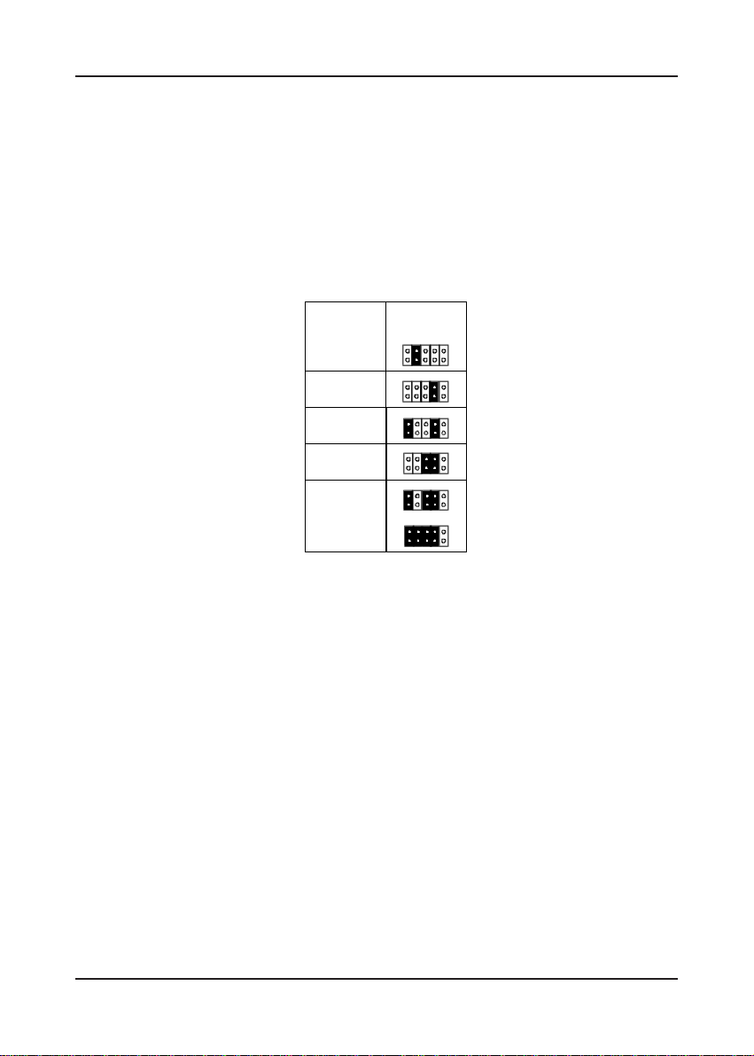
Voltage Configuration
There are two major processor types in general use--single and dual voltage processors.
Most single voltage processors such as Pentium, AMD-K5, and Cyrix 6x86 processors
use a single voltage value of 3.5v for both core and I/O voltage settings. Most dual
voltage processors such as Pentium processors with MMX technology and Cyrix
6x86L processors use a dual voltage value of 2.8v for core and 3.3v for I/O voltage
settings. To make the voltage setting for single and dual voltage processors, simply
set JP10 according to the table on the next page. The voltage range supported by
this mainboard is detailed in Figure 2-5 below.
Vcore JP10
2.2V
2.8V
1
1
2.9V
3.2V
3.3V
3.5V
Figure 2-5 Voltage Jumper Settings
1
1
1
1
8
Page 13
Hardware Setup
CPU-type
P54C-90, K5-PR90
P54C-120, K5-PR120
@90MHz
P54C-150, K5-PR150
@105MHz
Intel/
AMD
P54C-100, K5-PR100
P54C-133, K5-PR133
@100MHz
P54C-166, K5-PR166
@116.7MHz
P54C-200 x3
Pentium w/MMX 166MHz
Intel
Pentium w/MMX 200MHz x3
Pentium w/MMX 233MHz x3.5
6x86-PR150 @120MHz
6x86-PR166 @133MHz
6x86L-PR166 @133MHz
6x86L-PR200 @150MHz 75
Cyrix
6x86MX-PR166 @150MHz
6x86MX-PR166 @133MHz
6x86MX-PR200 @166MHz x2.5
6x86MX-PR200 @150MHz 75 x2
K6/166
K6/200 x3
AMD
K6/233 3.2 x3.5
+
+
+
+
+
+
+
+
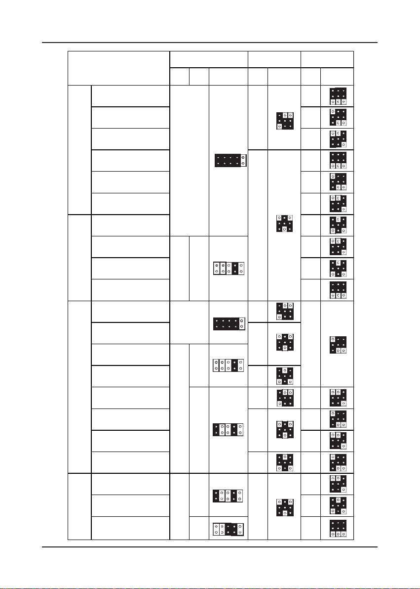
CPU Power Voltage System freq. Freq. ratio
I/O
Core
Vcc
3.5
JP10 MHz JP3~JP5
Vcc
1
60
66
1
3.3 2.8
1
3.5
60
66
1
2.8
60 x2.5
3.3
1
2.9
66
1
2.9
3.3
66
1
Spee
JP6~JP8
rate
1
x1.5
1
1
x2
x2.5
x1.5
x2
x2.5
x2.5
1
1
1
1
1
1
1
1
1
1
1
1
x2
1
1
1
1
1
x2
1
x2.5
1
1
1
1
1
1
9
Page 14
Chapter 2
2-4 Connector and Jumper Settings
Connectors are used to link the system board with other parts of the system, including
the power supply, the keyboard, and the various controllers on the front panel of
the system case.
The power supply connector is the last connection to be made while
installing a mainboard. Before connecting the power supply, please
make sure it is not connected to the power source.
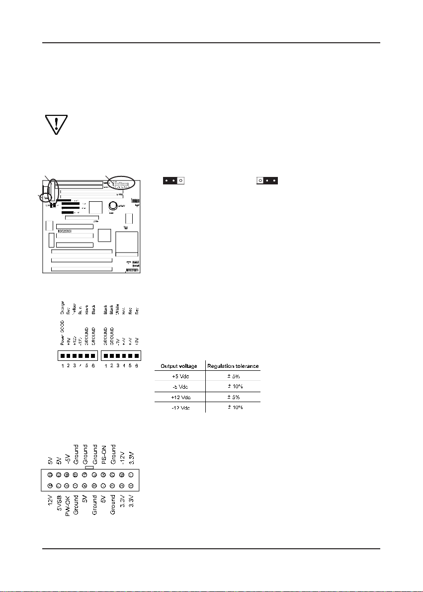
AT/ATX Power Supply Jumper (JP1)
CN2
JP1
CN5
1 1
ATX PowerAT Power
This mainboard supports two kinds of power connectors
and requires a power supply of at least 200 watts. If you
want to use an AT power supply, short pins 1 and 2 with the
jumper cap. If you want to use an ATX power supply, short
pins 2 and 3 with the jumper cap.
AT Power Supply Connector (CN2)
Most power supplies have two sets of six-wire leads.
Making sure the black wires of each lead are in the center,
plug both leads into the AT power supply connector. The
power supply requirement is as follows:
10
ATX Power Supply Connector (CN5)
The ATX power supply provides a single 20-pin connector
interface which incorporates standard +/-5V, +/-12V,
optional 3.3V and soft-power signal.
The Soft-power signal, a 5V trickle supply of at least
10mA, is continuously supplied when AC power is
available. When the system is in the Soft-Off mode, this
trickle supply maintains the system in it's minimum power
state.
Page 15
Hardware Setup
Software Power-Off Control
This mainboard can be powered down using theWindows 95 Software Power-Off
function. To power down your computer, click the START button on the Windows 95
task bar. Select "Shut Down The Computer" and the system turns off. The message "It
is now safe to turn off your computer" will not be shown when using this function.
Power-On By Modem
While in Soft-off state, if an external modem ring-up signal occurs, the system turns
on and can be remotely accessed. Please enable the Power on by Modem function in
BIOS's Power Management menu to activate this function. (See Section 3-4)
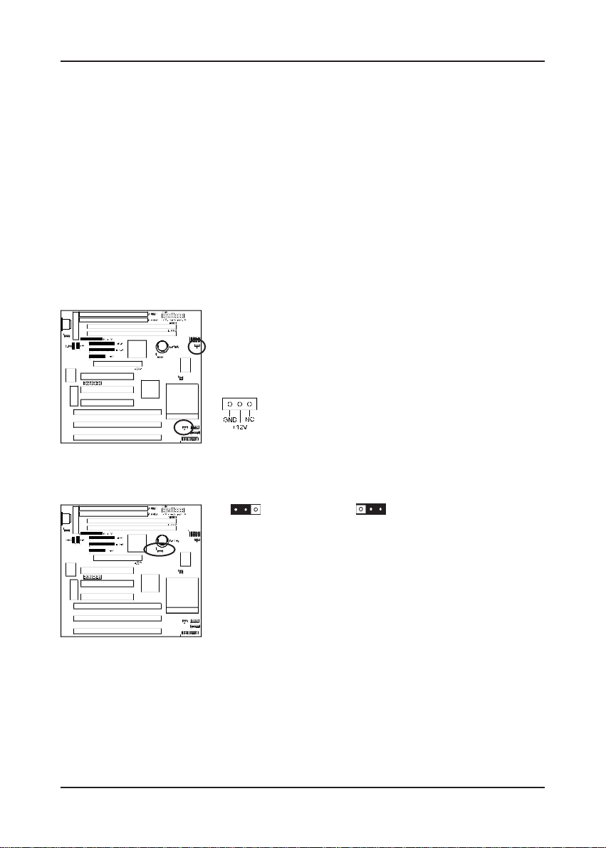
CPU/System Cooling Fan Connectors (CPUFAN/SYSFAN)
These added connectors allow the fans to draw their
power from the mainboard instead of the disk drive
connector. These fan connectors are available because
some systems have all the disk drive power connectors
in use.
Clear CMOS Data Jumper (JP2)
11
To clear the contents of the CMOS, please follow the
steps below.
1. Disconnect the system power supply from the power
2. Set the jumper cap at location 2~3 for 5 seconds, then
3. Connect the system's power and then start the system.
4. Enter BIOS, load the setup default settings in the
Default Clear CMOS Data
source.
set back to the default position.
CMOS Setup Utility Menu and then set the system
configuration in the Standard CMOS Setup menu.
11
Page 16
Chapter 2
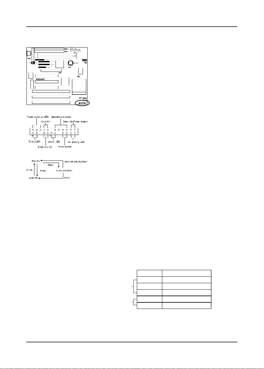
Front Panel Connector Set (CN7) A through G
A. Over-ride Power Button Connector
The power button on the ATX chassis can be used as a
normal power switch as well as a button to activate
Advanced Power Management Suspend mode. This mode
is used for saving electricity when the computer is not in
use for long periods of time. The Soft-OFF by PWRBTN
function in BIOS's Power Management Setup must set to
"Delay 4 Sec." to activate this function.
(See Section 3-4)
When the Soft-off by PWRBTN function is enabled,
pushing the power button rapidly will switch the system
between Full-On and Suspend mode. Pushing the button
rapidly again or any occurence of external activity such as
pressing a key on the keyboard will bring the system back
to Full-On. Pushing the button while in Full-On for more
than 4 seconds will switch the system to Soft-off and
pushing the button again rapidly will turn the system back
Over-ride Power
Button Operation
to Full-on. See Over-ride Power Button Operation
diagram.
B. Keyboard Lock & Power Indicator LED
Connector
Plugging this connector into the lock on the front panel
of the system case allows the lock to enable or disable
the keyboard. This function provides limited security
against casual intruders. The power indicator LED shows
the system's power status and willl flash when the system
is in Green mode (Suspend).
12
Power indicator LED
Keyboard Lock
Pin Definition
1 +5V DC
2 Not Connected
3 Ground
4 Keylock
5 Ground
Page 17

Hardware Setup
C. Green Switch/Green LED Connector
Some ATX cases provide a Green switch which is used to
put the system in Suspend mode. In suspend mode, the
power supply to the system is reduced to a trickle, the
CPU clock is stopped, and the CPU core is in it's minimum
power state. The system is woken up whenever the
keyboard or mouse is touched or the Green button is
pressed again. The system resumes in different ways as
defined by "Power Management Setup" screen in BIOS.
D. Speaker Connector
Pin Definition
1 Speaker Signal
2 GND
3 GND
4 +5V DC
E. System Reset Switch Connector
This connector should be connected to the reset switch
on the front panel of the system case. The reset switch
allows you to restart the system without turning the
power off.
Pin Definition
1 System
2 GND
F. IDE Activity LED Connector
The IDE activity LED lights up whenever the system
reads/writes to the IDE devices.
G. Turbo LED Connector
This mainboard does not have turbo/de-turbo speed mode.
Even though this function does not exist, the turbo LED
will light when the LED is connected and the turbo button
is pressed.
Change CPU Speed with the Keyboard
Use the following commands to change the CPU speed between turbo/de-turbo.
Set to low speed [CTRL] [ALT] [-]
Set to high speed (turbo) [CTRL] [ALT] [+]
13
Page 18
Chapter 2
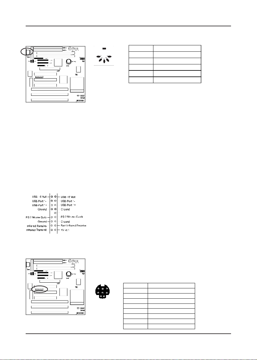
AT Keyboard Connector (J2)
Pin Definition
1 Keyboard Clock
2 Keyboard Data
3 (None)
4 Ground
5 +5V DC
Keyboard Connector/Pin Definitions
Poly-fuse Over Current Protection
The poly-fuse protects the system from dangerous voltages the system might be
exposed to via the keyboard or USB connectors. In case of such exposure, the polyfuse will immediately be disconnected from the circuit, just like a normal fuse. After
being disconnected for a certain period of time, the poly-fuse will return to its
normal state, after which the keyboard or USB can function properly. Unlike
conventional fuses the poly-fuse will not have to be replaced, relieving the user
wasted time and inconvenience.
USB Kit Connector (CN1) A through C
The USB Kit connector is a combination of of USB, PS/
2 mouse, and Infrared functions grouped on the same
connector. The USB Kit (Figure 1-5) is installed in a back
panel of the chassis and is connected to the USB Kit
connector with an 18-pin cable.
14
A. Infrared Connector
If the IR Address Select function in BIOS's Integrated
Peripherals menu is not set at disabled, the COM2 port
will support IR functions. (See Section 3-7)
Pin Definition
1 Ir-Tx
2 Ir-Rx
3 Not Connected
4 Vcc (+5V)
5 GND
6 Not Connected
7 Not Connected
8 Not Connected
Page 19
Hardware Setup
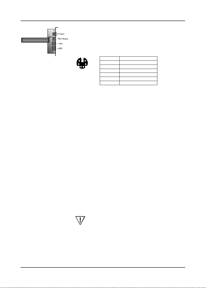
B. PS/2 Mouse Connector
If a PS/2 mouse is used, BIOS will automatically detect
and assign IRQ12.
546
132
Pin Definition
1 Data
2 Not Connected
3 Ground
4 +5V (fused)
5 Clock
6 Not Connected
C. Dual Channel USB(Universal Serial Bus)
Connector
Enable the OnChip USB function in BIOS's Integrated
Peripherals Menu if you want to use a USB keyboard.
(See Section 3-7) Other USB devices do not require the
enabling of this function. USB is an open industry standard,
providing a simple and inexpensive way to connect up to
125 devices to a single computer port. Keyboards, mice,
tablets, digitizers, scanners, bar-code readers, modems,
printers and many more can all be used at the same time.
USB is a dynamically reconfigurable serial bus with an
elementary data rate of 12Mbps, based on off the shelf,
low cost micro-controller technology. It's modular layered
software protocol supports sophisticated devices and
application programs.
This board contains a USB Host controller and includes
a root hub with two USB ports (meets USB Rev 1.0 spec.).
Two USB peripherals or hub devices are able to be
connected.
Compatibility with different USB peripherals is
still being tested.
15
Page 20
Chapter 2
2-6 Main Memory Configuration
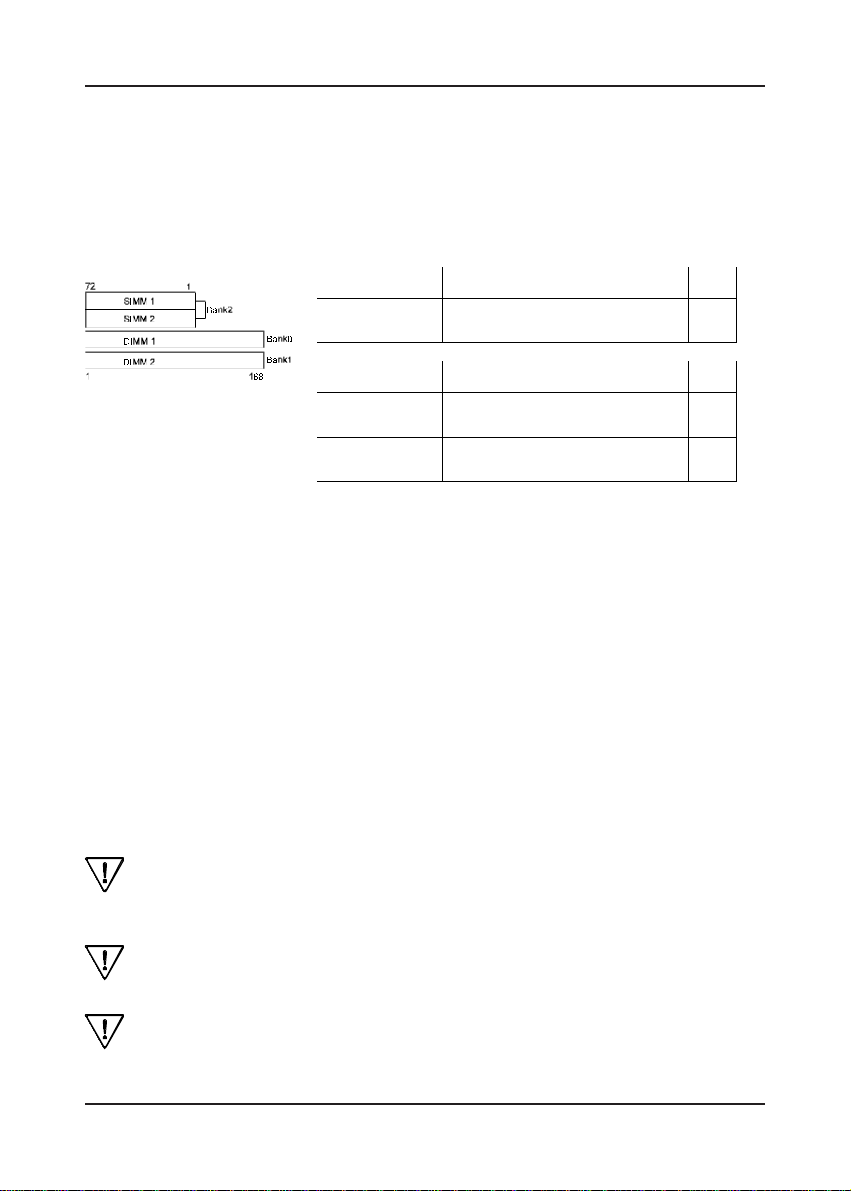
The DRAM memory system on board consists of 3 banks, and the memory range is
8 ~ 256 MBytes. You must install 2 SIMM modules(same size, same speed, either
single or double sided) in each bank at a time. It does not matter which bank you
install first.
SIMM 72-pin 5V SIMM Qty.
Bank2
(SIMM1,SIMM2)
DIMM 168-pin 3.3V unbuffered DIMM Qty.
Bank0 (DIMM1)
Bank1 (DIMM2)
DRAM Specifications
Types Supported FP(Fast Page), EDO(Extended Data Output) and
Synchronous DRAM
Speed requirement FP/EDO: 70-ns (or faster) for 50 or 60MHz system
SDRAM: 10/12ns
4/8/16/32/64 FPM or EDO SIMM
(DIMM sockets must be empty)
8/16/32/64/128 MB EDO or SDRAM
(SIMM sockets must be empty)
8/16/32/64/128 MB EDO or SDRAM
(SIMM sockets must be empty)
x2
x 1
x 1
frequency and 60-ns for 66MHz system
frequency.
Module types & sizes 4/8/16/32/64 MBytes, single/double-sided, 5v SIMM
8/16/32/64 MBytes, single/double-sided, 3.3v DIMM
Parity Both parity and non-parity modules may be used
however the parity function is not supported by this
mainboard.
Most SDRAM will be 3.3V only (i.e. SDRAM I/O pins will not be 5V
tolerant). It is not recommended to mix 3.3V EDO/SDRAM DIMM with
5V EDO/FPM SIMM.
Because 64/128MB DIMM is not yet mainstream, the compatibility of 64/
128MB DIMM can not be 100% guaranteed.
Due to loading anomalies, using DIMM with an 'n x 4' DRAM base on this
mainboard is not recommended. For example, a DIMM that uses sixteen
16Mb x 4 devices should not be used.
16
Page 21
Hardware Setup
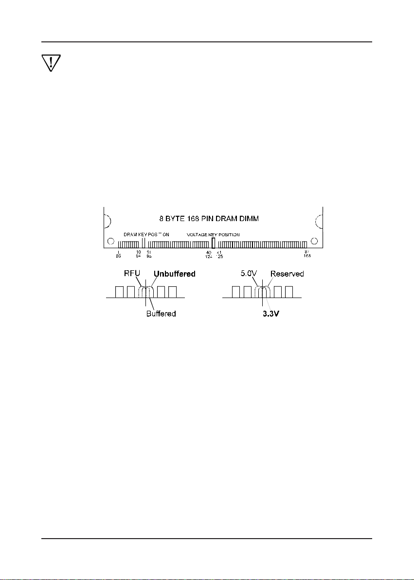
This mainboard supports 3.3v, unbuffered, 4-clock, SDRAM DIMM only.
Buffered, 5V, or 2-clock SDRAM DIMMs should not be used.
This board has two DIMM (Dual-in-line Memory Module) sockets to support
SDRAM type DRAM and has the better optimized read timings (7-1-1-1).
The DIMM sockets will quickly replace SIMM as the next module standard
for the PC industry and will become the memory subsystems standardized 64bit data interface. Recently, JEDEC committee passed the unbuffered DIMM
pinout specification as a standard for higher speed transfer. The unbuffered
DIMM allows for SDRAM, EDO and FPM DRAM compatibility as well as
pinouts for x64, x72 with parity, x72 with ECC and x80 ECC. The unbuffered
DIMM is distinguished by the keyed notch lying to the right of the centerline
of the DRAM key position as shown in the figure below.
17
Page 22

Chapter 2
- Memo
18
Page 23

Award BIOS Setup Program
Chapter 3
3
Award BIOS Setup Program
Award's BIOS ROM has a built-in setup program that allows users to modify the basic
system configuration. This information is stored in CMOS RAM so that it can retain
the setup information, even when the power is turned off.
When you turn on or reboot the system, press the Delete key to enter the Award
BIOS setup program. The primary screen as shown in Figure 3-1 is a list of the menus
and functions available in the setup program. Select the desired item and press enter
to make changes. Operating commands are located at the bottom of this and all other
BIOS screens. When a field is highlighted, on-line help information is displayed on
the left bottom edge of the screen.
ROM PCI / ISA BIOS (2A5LEC39)
CMOS SETUP UTILITY
AWARD SOFTWARE, INC.
STANDARD CMOS SETUP
BIOS FEATURES SETUP
CHIPSET FEATURES SETUP
POWER MANAGEMENT SETUP
PNP/PCI CONFIGURATION
LOAD SETUP DEFAULTS
E SC : Quit
F10 : Save & Exit Setup
Figure 3-1 Setup Program Initial Screen
INTEGRATED PERIPHERALS
SUPERVISOR PASSWORD
USER PASSWORD
IDE HDD AUTO DETECTION
SAVE & EXIT SETUP
EXIT WITHOUT SAVING
: Select Item
(Shift) F2 : Change Color
Time, Date, Hard Disk T ype...
19
Page 24
Chapter 3
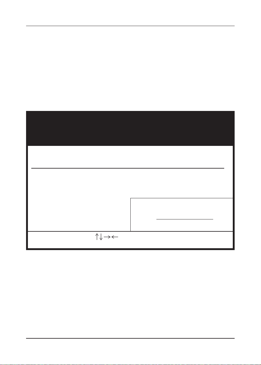
3-1 Standard CMOS Setup
The Standard CMOS Setup allows users to configure system components such as
hard disk drive, floppy disk drive and video display as well as date, time and bootup error signaling. This configuration menu should be changed when installing a
mainboard for the first time, changing hardware in your system such as the HDD,
FDD, video display, or when the CMOS data has been lost or contaminated. Choose
the Standard CMOS Setup option from the CMOS Setup Utility menu (Figure 3-1)
to display the following screen. When a field is highlighted, on-line help information
is displayed on the left bottom edge of the screen.
ROM PCI / ISA BIOS (2A5LEC39)
STANDARD CMOS SETUP
A WARD SOFTWARE, INC.
Date (mm : dd : yy) : Fri, July 25 1997
Time (hh : mm : ss) : 9: 14: 43
HARD DISKS TYPE SIZE CYLS HEAD PRECOMP LANDZ SECTOR MODE
Primary Master : Auto 0 0 0 0 0 0 Auto
Primary Slave : Auto 0 0 0 0 0 0 Auto
Secondary Master : Auto 0 0 0 0 0 0 Auto
Secondayt Slave : Auto 0 0 0 0 0 0 Auto
Drive A : 1.44M, 3.5 in.
Drive B : None
Video : EGA/VGA
Halt On : All Errors
Base Memory :
Extended Memory :
Other Memory :
Total Memory :
640K
15360K
384K
16384K
E SC : Quit
F1 : Help
(Shift) F2 : Change Color
Figure 3-2 Standard CMOS Setup Screen
: Select Item
PU/PD/+/- : Modify
Date/Time
Set the date and time. Do not skip this function as all of your timed events such
as power management, saving files, etc. are based on this timer.
Hard Disk Setup (Primary/Secondary; Master/Slave)
This category identifies up to four IDE hard disk drives that have been installed in
the computer. This section does not show information on other IDE devices such
as CD-ROM drives or other hard drive types such as SCSI drives.
20
Page 25

Award BIOS Setup Program
Type (Auto/User/None): Use the fields under the Type column to determine the method
you will use to configure the IDE devices. If you choose Auto, BIOS will automatically
detect and make optimal settings for most IDE hard drives.
The mainboard manufacturer recommends that you choose Auto for all
drives.
Choose User to define your own drive type manually. You must enter values indicated
in the table below into each drive parameter field. This information should be included
in the documentation from your hard disk vendor or system manufacturer:
TYPE Setting method
CYLS Number of cylinders
HEAD Number of heads
PRECOMP Write precompensation cylinder
LANDZ Landing zone
SECTOR Number of sectors
MODE Mode type
Table 3-1 Hard Disk Drive Parameters
Cyls/Head/Sector: The number of Cylinders, Heads, and Sectors can usually be found
written on the top of the hard disk. If you have a relatively new hard drive, entering
this information alone is usually sufficient for normal hard disk operation. The hard
disk will not work properly if you enter improper information for these categories.
Precomp: Older hard drives (i.e., MFM or RLL drives) have the same number of sectors
per track at the innermost tracks as at the outermost tracks. Thus, the data density
at the innermost tracks is higher and the bits are lying closer together. Even though
the physical size of a sector gets progressively smaller as the track diameter diminishes,
each sector must still hold 512 bytes. Write precompensation circuitry compensates
for the difference in sector size by boosting the write current for inner track sectors.
Landz: This defines the address of the landing zone and is only used for older hard
drives which do not have an auto-parking feature.
Mode: If the Type value is not None for any device, you must set the Mode value
for that device. There are four different Mode values: Auto, Normal, Large, and
LBA.
Auto - BIOS detects and enters the IDE drive type during bootup.
Normal - for IDE drives that meet the old IDE specification which support a
maximum capacity of 528MB (1024 cylinders, 16 heads, and 63 sectors).
Large - for IDE drives that do not support LBA and have more than 1024
cylinders. Try this setting if your hard disk does not operate properly with
21
Page 26

Chapter 3
the LBA setting. Large mode is not supported by all operating systems, i.e.,
only certain versions of DOS support large mode.
LBA - (Large/Logical Block Addressing) With LBA, the IDE controller
transforms the data address described by sector, head, and cylinder number
into a physical block address, significantly improving data transfer rates. This
mode is for drives with greater than 1024 cylinders and between 528MB and
8.4GB in size. This protocol is the current common standard.
Choose None for Type if there are no IDE HDD devices in your system.
You can use the IDE HDD Auto Detection function to auto detect your hard
@
drive parameters. Using this function will automatically insert the parameters
discussed under Hard Disk Setup and will indicate User for the Field value.
Please see Section 3-9 for more information.
Floppy Disk Drives
Choose the memory capacity and disk size that corresponds with that of your floppy
disk drive(s).
Video
Select the type of video adapter present in your system. You can ignore this setting
if you are using a VGA monitor since VGA BIOS automatically configures this setting.
Halt
When the system is powered on, BIOS performs a series of diagnotic tests called
POST (Power On Self Test). This function stops the computer if BIOS detects a
hardware error. You can tell BIOS to halt on all errors, no errors, or not to halt on
specific errors.
22
Page 27

Award BIOS Setup Program
3-2 BIOS Features Setup
By choosing the BIOS Features Setup option from the CMOS Setup Utility menu
(Figure 3-1), the screen below is displayed. This sample screen contains the
manufacturer's default values for the mainboard.
ROM PCI / ISA BIOS (2A5LEC39)
BIOS FEATURES SETUP
A WARD SOFTWARE, INC.
Virus Warning : Disabled
CPU Internal Cache : Enabled
External Cache : Enabled
Quick Power On Self Test : Enabled
Boot Sequence : A,C,SCSI
Swap Floppy Drive : Disabled
Boot Up Floppy Seek : Enabled
Boot Up NumLock Status : On
Boot Up System Speed : High
Typematic Rate Setting : Disabled
Typematic Rate (Chars/Sec) : 6
Typematic Delay (Msec) : 250
Security Option : Setup
PCI/VGA Palette Snoop : Disabled
OS Select(For DRAM>64MB): Non-OS2
Figure 3-3 BIOS Feature Setup Screen
Video BIOS Shadow : Enabled
C8000 - CBFFF Shadow : Disabled
CC000- CFFFF Shadow : Disabled
D0000 - D3FFF Shadow : Disabled
D4000 - D7FFF Shadow : Disabled
D8000 - DBFFF Shadow : Disabled
DC000- DFFFF Shadow : Disabled
ESC : Quit
F 1 : Help
F5 : Old Values
F7 : Load Setup Defaults
PU/PD/+/- : Modify
(Shift) F2 : Color
:Select Item
A. VIRUS PROTECTION
Virus Warning
When Enabled, BIOS activates a warning message to the user when any program
(i.e., a virus) attempts to access the boot sector or hard disk partition table. The
user is able to intervene by running an anti-virus program. This function only
protects the boot sector and not the entire hard drive.
B. CACHE CONTROL
CPU Internal Cache/External Cache
Cache memory is much faster than conventional DRAM system memory. These
fields allow you to enable or disable the CPUs Level 1 built-in cache and Level
2 external cache. Both settings are left enabled to significantly increase the
performance of your computer.
23
Page 28

Chapter 3
C. BOOT UP FEATURES
After turning on the system, BIOS will perform a series of device initializations
and diagnostic tests discussed below.
Quick Power On Self Test (POST)
Enable this function to reduce the amount of time required to run the POST
(Power On Self Test). BIOS saves time by skipping some items during POST.
It is recommended that you disable this setting. Discovering a problem during
bootup is better than loosing data during your work.
Boot Sequence
This option sets the sequence of drives BIOS attempts to boot from after POST
completes. BIOS will search these drives for an operating system.
Swap Floppy Drive
Enabling this function will swap the floppy drive assignment so that drive A
will function as drive B, and drive B will function as drive A. Note that the
boot sequence assignment mentioned directly above does not inlcude booting
from floppy drive B. This function is useful if floppy drives B and A are of
a different format and you want to boot from floppy drive B.
Boot up Floppy Seek
During POST, BIOS will determine if the installed floppy disk drive has 40
or 80 tracks. A 360K drive has 40 tracks and 720K, 1.2M and 1.44M drives
have 80 tracks. All modern floppy disk drives have 80 tracks.
Boot Up NumLock Status
This function defines the keyboard's numberpad as number keys or arrow keys.
Boot Up System Speed
This function determines the CPU speed while in non-protected mode under
DOS. Set to High for regular CPU speed and low for decreased CPU speed.
This function is used for applications such as games that require decreased
CPU speed.
D. KEYBOARD INTERFACE
Typematic Rate Setting
When enabled, you can set the following two typematic control items. When
disabled, keystrokes are determined arbitrarily by the keyboard controller in
your system.
Typematic Rate (Chars/Sec)
The typematic rate sets the rate at which characters on the screen repeat when
a key is pressed and held down.
24
Page 29

Award BIOS Setup Program
Typematic Delay (Msec)
The typematic delay sets how long after you press a key that a character begins
repeating.
E. Security Option
The Supervisor and/or User Password functions shown in Figure 3-1 must be set
to take advantage of this function. See Section 3-8 for password setting information.
When the Security Option is set to System, a password must be entered to boot
the system or enter the BIOS setup program. When the Security Option is set
to Setup, a password is required to enter the BIOS setup program.
F. PCI/VGA Palette Snoop
Some non-standard VGA cards or MPEG video cards may not show colors
properly. Setting this function to Enabled can correct this problem.
G. OS Select (For DRAM > 64MB)
If your system's DRAM is larger than 64MB and you are running OS/2, select
OS/2 as the item value. Otherwise, set the item value to Non-OS/2 for all other
operating systems.
H. Shadow Memory
Software such as system BIOS, video BIOS, SCSI BIOS, etc that resides in ROM
(Read Only Memory) chips is called firmware. Shadowing of firmware occurs
when BIOS is copied to RAM address C0000h through DFFFFh. Video BIOS
loads into the C0000-C7FFF memory area when video shadowing is enabled. If
an expansion peripheral in your system contains ROM-based firmware, you need
to know the address range the ROM occupies to shadow it into the correct area
of RAM.
Shadowing improves the firmware's performance because the firmware can be
read by the CPU through the 16- or 32-bit DRAM bus as opposed to the 8-bit
XT bus. However, shadowing also results in reducing the amount of high memory
(640 KB to 1 MB) for loading device drivers. Shadowing is used mostly for
ROM chips on ISA cards and not for PCI cards. Shadowing and playing games
at the same time may result in system instability as some games access the RAM
memory area being shadowed.
25
Page 30
Chapter 3
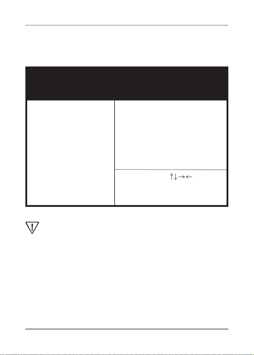
3-3 Chipset Features Setup
By choosing the Chipset Features Setup option from the CMOS Setup Utility menu
(Figure 3-1), the screen below is displayed. This sample screen contains the
manufacturer's default values for the mainboard.
ROM PCI / ISA BIOS (2A5LEC39)
CHIPSET FEATURES SETUP
A WARD SOFTWARE, INC.
DIMM 1 EDO/SDRAM Timing : 70/12 ns
DIMM 2 EDO/SDRAM Timing : 70/12 ns
SIMM 3 EDO/FP DRAM Timing: 70 n s
SDRAM Cycle Length : 3
DRAM Read Pipeline : Enabled
Cache Strategy : WT
Cache Rd+CPU Wt Pipeline : Enabled
Read Around Write : Enabled
Cache Timing : Fastest
Video BIOS Cacheable : Enabled
System BIOS Cacheable : Enabled
Memory Hole At 15MB Addr. : Disabled
AGP : Enabled
AGP Aperture Size : 64M
AGP-2X Mode : Enabled
Figure 3-4 Chipset Features Setup Screen
Flash BIOS Protection : Disabled
CPU Warning Temperature : 65
Current CPU Temperature : 25
Current CPUFAN Speed : 3600 RPM
Current SYSFAN Speed : 3600 RPM
Current Vin (V) : 3.3
ESC : Quit
F 1 : Help
F5 : Old Values
F7 : Load Setup Defaults
PU/PD/+/- : Modify
(Shift) F2 : Color
o
C/140 oF
o
C/77 oF
:Select Item
All of the above settings have been determined by the mainboard manufacturer
and should not be changed unless you are absolutely sure of what you are doing.
Explanation of the DRAM timing and chipset features setup is lengthy, highly
technical and beyond the scope of this manual. Below are abbreviated descriptions
of the functions in this setup menu. You can look on the world wide web
for helpful chipset and RAM configuration information including AWARD's
web site at http://www.award.com.
A. Video BIOS Cacheable
Enabling this function allows caching of the video BIOS ROM at C0000h-C7FFFh,
resulting in better video performance. However, if any program writes to this
memory area, a system error may result. Caching the video BIOS results in better
performance than shadowing the video BIOS as discussed in Section 3-2.
26
Page 31

Award BIOS Setup Program
B. System BIOS Cacheable
Enabling this function allows caching of the system BIOS ROM at F0000hFFFFFh, resulting in better system performance. However, if any program writes
to this memory area, a system error may result. Caching the system BIOS results
in better performance than shadowing the system BIOS as discussed in Section
3-2.
C. Memory Hole at 15MB Addr.
Enabling this feature will reserve the 15MB to 16MB memory address space for
ISA expansion cards. However, enabling this function will result in not allowing
the system to have access to memory above 16MB. Please note that some
expansion cards require this setting to be enabled. The default setting is Disabled.
D. AGP
This function must be enabled when using an AGP card. If you disable this function
you can still use an AGP card. However, the AGP card will only have PCI card
performance.
E. AGP Aperture Size
This function determines the amount of system memory that is given to the AGP
card. Options range from 4MB to 256MB. This is a dynamic memory allotment
in that the AGP card will only use the amount of memory that it needs. The
remaining memory not in use will be available for the system to use. For example,
if 16MB is alloted to the AGP card and the card only needs 8MB, the remaining
8MB will be available for system use.
F. AGP-2X Mode
Enable this setting to utilize the 2X mode (twice as fast as 1X) offered by advanced
AGP cards. Your VGA card must support 2X mode in order to take advantage
of the faster speed.
G. Flash BIOS Protection
The mainboard manufacturer developed BIOS protection technology that protects
the System BIOS from accidental corruption by unauthorized users or computer
viruses. When enabled, the BIOS data cannot be changed when attempting to update
BIOS with the the FLASH utility. When disabled, the BIOS data can be updated
by using the FLASH utility.
H. System Monitoring and Alerting (Optional)
These optional system health monitoring features are available when an EISCA
v1.0 compliant fan is connected to the Fan 78 connector on your mainboard.
Change the CPU warning temperature according to the specifications of your CPU.
For more information about EISCA fans, see Apendix II of this manual.
27
Page 32
Chapter 3
3-4 Power Management Setup
This section provides information on the Green PC power management funtcions.
In order to enable the power management functions, please select the Power Management
Setup option from the CMOS Setup Utility menu (Figure 3-1). This sample screen
contains the manufacturer's default values for the mainboard.
ROM PCI / ISA BIOS (2A5LEC39)
POWER MANAGEMENT SETUP
A WARD SOFTWARE, INC.
Power Management : Disabled
PM Control by APM : Yes
Video Off Option : Suspend -> Off
Video Off Method : V/H SYNC+Blank
MODEM Use IRQ : 3
Soft-Off by PWRBTN : Instant-Off
** PM Timers **
HDD Power Down : Disabled
Doze Mode : Disabled
Suspend Mode : Disabled
** PM Events **
VG A : OFF
LPT & COM : LPT/COM
HDD & FDD : ON
DMA/Master : OFF
Power On By Modem : Disabled
Power On By Alarm : Disabled
ESC : Quit
F 1 : Help
F5 : Old Values
F7 : Load Setup Defaults
:Select Item
PU/PD/+/- : Modify
(Shift) F2 : Color
Figure 3-5 Power Management Setup Screen
A. Power Management
Power management allows the computer to save electricity when it is not in use
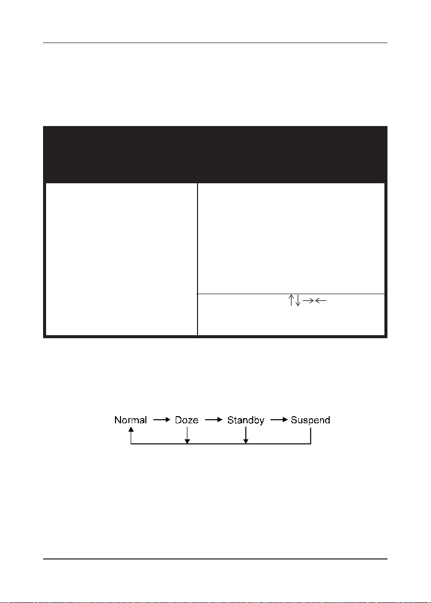
by entering increasingly deep power saving modes as shown by the diagram below.
Figure 3-6 Power Saving Mode Flow Chart
The computer runs in Normal operation mode until the Doze timer expires, at
which point the computer enters Doze mode. If no external activity occurs, the
computer will go into Standby and Suspend modes when their respective timers
expire. If external activity occurs, the computer will wake up from Power
Management and return to Normal mode. To activate the function, set Power
Management to Maximum Saving, User Define, or Minimum Saving described
28
Page 33

Award BIOS Setup Program
below. For a description of the power saving modes (Doze, Standby, and
Suspend) see their descriptions below.
Disabled - Turns off the Power Management functions.
Max. Saving - All timers are set at the minimum value of one minute to
maximize power saving.
Min. Saving - All timers are set at the maximum value of one hour for
minimal power saving.
User Define - User can configure the timer to a desired time according to
the values available.
Note that enabling the Power Management function will result in enabling
the HDD Power Down function (Max Saving = 15 min, Min Saving = 1 min).
The HDD Power Down function is not part of the Power Management scheme
as indicated in Figure 3-6 Refer to the Standby Mode, Suspend Mode, and
HDD Power Down descriptions below for more informaiton on hard drive
power management.
B. PM Control by APM
This function allows software other than BIOS to control Power Management
features Enable this function in BIOS and make sure APM (Advanced Power
Management) is present. For example, run the Power utility program located
in the DOS directory, C:\DOS\POWER.EXE to use Power Management features
under DOS. For Windows 3.1x and Windows 95, you need to install Windows
with the APM feature.
C. Video Off Option
This setting determines when the monitor enters power saving mode. As the
function name indicates, the monitor enters the power saving mode after the
chosen event expires. The Power Management function must be enabled to use
this function.
D. Video Off Method
This function serves as both a screen saver and power saver for monitors.
See the next function, Video Off After, for setting the video timer.
Blank - BIOS will only blank the monitor's screen. The electricity saved in
this mode is negligible and this function is only used as a screen saver to
prevent screen damage while the screen is on but not in use.
V/H SYNC+Blank - The system turns off the vertical and horizontal synchronization ports, writes blanks to the VGA buffer and the monitor's electron
gun turns off. This function requires a monitor with Green features in order
to take advantage of the power saving function. If you enable this function
and do not have a Green monitor, the result will be the same as if you had
29
Page 34

Chapter 3
selected Blank. This function serves as both a screen saver and an electricity
saver.
DPMS Supported - Select this option if your video card supports the Display
Power Management Signaling (DPMS) standard (i.e., you have a monitor that
supports Green features). Use software supplied by your video subsystem
to set video power management options.
E. Modem Use IRQ
If your computer has a modem, use this function to tell BIOS which IRQ is being
occupied by the modem card. When the system is in Green mode, the modem
requires an IRQ assignment to wake up the system and perform tasks. This
assignment is compliant with the APM 1.2 specification and is to be used in
coordination with APM 1.2 compliant operating systems.
F. Soft-Off by PWRBTN
When Enabled, this function allows the power button to put the system in Suspend,
a power saving mode. See section 2-4 for operation instructions of the power
button.
G. HDD Power Down
To enable this function, make sure the Power Management function is not set
to disabled. When the HDD idle time has elapsed, BIOS sends a command to
the hard disk to turn off the motor. Set a time between 1 and 15 to indicate
time required to wait before the hard drive enters a power saving mode. Some
old hard drives may not support this function.
H. Doze Mode
To enable this function, make sure the Power Management function is not set
to disabled. If no interrupts have occured and the Doze timer expires, system
will enter Doze mode. In Doze mode, the CPU clock runs at a lower speed while
all other devices operate normaly.
Power saving modes achieved in lower power saving states will either be
@
maintained or enter higher power saving modes when switching to higher power
saving states. For example, the CPU clock will not switch back to normal
in Standby mode. It will maintain a decreased rate in Standby Mode and turn
off in Suspend Mode.
I. Suspend Mode
To enable this function, make sure the Power Management function is not set
to disabled. If the system runs in Dozemode and the Suspend timer expires, all
devices regulated by power management will shut off and the CPU speed will
be 0 MHz.
30
Page 35

Award BIOS Setup Program
J. Power On By Modem
When enabled, a modem that receives a call will wake up the system from Softoff or Green mode. To activate this function, you must leave your modem on
and use the Software Power off. See the Software Power-Off control description
in Section 2-4 of this manual.
K. Power On By Alarm
When enabled, this setting allows the system to turn back on at a designated time
of the month. User must designate date of month and time of day. This function
is only available when using an ATX pwer supply and Software Power-Off. See
the Software Power-Off control description in Section 2-4 of this manual.
31
Page 36
Chapter 3
3-5 PNP/PCI Configuration
This section provides IRQ and DMA setting information. By choosing the PnP/PCI
Configuration option from the CMOS Setup Utility menu (Figure 3-1), the screen
below is displayed. This sample screen contains the manufacturer's default values
for the mainboard.
ROM PCI / ISA BIOS (2A5LEC39)
PNP/PCI CONFIGURA TION
A WARD SOFTWARE, INC.
PNP OS Installed : No
Resources Controlled By : Manual
Reset Configuration Data : Disabled
IRQ-3 assigned to : Legacy ISA
IRQ-4 assigned to : Legacy ISA
IRQ-5 assigned to : PCI/ISA PnP
IRQ-7 assigned to : Legacy ISA
IRQ-9 assigned to : PCI/ISA PnP
IRQ-10 assigned to : PCI/ISA PnP
IRQ-11 assigned to : PCI/ISA PnP
IRQ-12 assigned to : PCI/ISA PnP
IRQ-14 assigned to : Legacy ISA
IRQ-15 assigned to : Legacy ISA
DMA-0 assigned to : PCI/ISA PnP
DMA-1 assigned to : PCI/ISA PnP
DMA-3 assigned to : PCI/ISA PnP
DMA-5 assigned to : PCI/ISA PnP
DMA-6 assigned to : PCI/ISA PnP
DMA-7 assigned to : PCI/ISA PnP
Figure 3-6 PCI & ONBOARD I/O Setup Screen
CPU to PCI Write Buffer : Enabled
PCI Parity Check : Disabled
PCI Delay Transaction : Enabled
FDD IRQ Can Be Free : No
Assign IRQ For VGA : Enabled
ESC : Quit
F 1 : Help
F5 : Old Values
F7 : Load Setup Defaults
PU/PD/+/- : Modify
(Shift) F2 : Color
:Select Item
A. PNP OS installed
If you want to install a PNP compatible OS (such as Windows 95) set to Yes.
B. Resources Controlled By
When set to Manual the system BIOS will not refer to the ESCD for IRQ & DMA
information. Instead, it will refer to the items in the setup menu for assigning
IRQ & DMA. When set to Auto the system BIOS will refer to the ESCD for
all legacy information.
32
ESCD(Extended System Configuration Data) provides a detailed format
of the configuration data structures stored in flash memory. Each data
structure defines the resources used by a device or a card in the system.
This includes legacy and PCI/ISA PnP devices.
Page 37

Award BIOS Setup Program
C. Reset Configuration Data
When Enabled the system BIOS will clear/reset the ESCD during POST. After
clearing the ESCD, the BIOS will then change this item's value to "Disabled."
Otherwise, the ESCD data would become useless.
D. IRQ#/DMA# assign to
When resources are controlled manually, you can assign each system interrupt
& DMA channel for "Legacy ISA" or "PCI/ISA PnP" card used. While using Legacy
ISA Cards (non-PnP ISA cards), please set the necessary corresponding resources
(INT#, DMA#) from "PCI/ISA PnP" to "Legacy ISA."
@ All ISA non-PnP devices are legacy devices that select resources
(I/O Addr., INT# or DMA#) by using hardware jumpers on these devices.
@ IRQ-3/4/7/12/14/15 have been set as default for on board devices (COM2,
COM1, Printer port, PS/2 mouse, IDE1 and IDE2).
E. FDD IRQ Can Be Free
This function allows users to choose if the FDD IRQ is able to be freed for use
with other processes that require IRQ.
F. Assign IRQ For VGA
This function allows BIOS to make an IRQ available to VGA cards. Current VGA
card models do not require this function to be enabled.
33
Page 38
Chapter 3
3-6 Load Setup Defaults
Load Setup Defaults loads the default system values directly from the CMOS Setup
Utility menu (Figure3-1). If the stored record created by the setup program becomes
corrupted and therefore unusable, these defaults will be loaded automatically when
you turn on the computer.
ROM PCI / ISA BIOS (2A5LEC39)
CMOS SETUP UTILITY
A WARD SOFTWARE, INC.
STANDARD CMOS SETUP
BIOS FEATURES SETUP
CHIPSET FEATURES SETUP
POWER MANAGEMENT SETUP
PNP/PCI CONFIGURATION
LOAD SETUP DEFAULTS
E SC : Quit
F10 : Save & Exit Setup
Load SETUP Defaults except Standard CMOS SETUP
Figure 3-7 Load Setup Defaults Screen
INTERGRATED PERIPHERALS
SUPERVISOR PASSWORD
USER PASSWORD
Load SETUP Defaults (Y/N)? N
IDE HDD AUTO DETECTION
SAVE & EXIT SETUP
EXIT WITHOUT SAVING
(Shift) F2 : Color
: Select Item
34
Page 39

Award BIOS Setup Program
3-7 Integrated Peripherals
This section provides information on setting peripheral devices. By choosing the
Integrated Peripherals option from the CMOS Setup Utility menu (Figure 3-1), the
screen below is displayed. This sample screen contains the manufacturer's default
values for the mainboard.
ROM PCI / ISA BIOS (2A5LEC39)
INTEGRA TED PERIPHERALS
A WARD SOFTWARE, INC.
OnChip IDE First Channel : Enabled
OnChip IDE Second Channel : Enabled
IDE Prefetch Mode : Enabled
IDE HDD Block Mode : Enabled
IDE Primary Master PIO : Auto
IDE Primary Slave PIO : Auto
IDE Secondary Master PIO : Auto
IDE Secondary Slave PIO : Auto
IDE Primary Master UDMA : Auto
IDE Primary Slave UDMA : Auto
IDE Secondary Master UDMA : Auto
IDE Secondary Slave UDMA : Auto
Onboard FDC Controller : Enabled
Onboard Serial Port 1 : 3F8/IRQ4
Onboard Serial Port 2 : 2F8/IRQ3
IR Address Select : Disabled
Figure 3-8 PCI & ONBOARD I/O Setup Screen
Onboard Parallel Port : 378/IRQ7
Parallel Port Mode : SPP
OnChip USB : Disabled
ESC : Quit
F 1 : Help
F5 : Old Values
F7 : Load Setup Defaults
PU/PD/+/- : Modify
(Shift) F2 : Color
:Select Item
A. On-chip Primary/Secondary PCI IDE
Disable these settings to turn off the built-in IDE controller.
B. IDE Prefetch Mode
This mode is involved in multiple sector read/writes and improves the performance
of your system. Enabling this function improves the performance of your
computer.
C. IDE HDD Block Mode
Enable this mode to improve the performance of your system. Block Mode is
also referred to as block transfer or multiple sector read/write. When this setting
is enabled, the maximum number of block read/writes per sector supported by
the the drive is detected. Most new hard drives support this mode.
35
Page 40

Chapter 3
D. On Board IDE Control
The following settings are used to configure the on-board IDE controller.
IDE Primary/Secondary Master/Slave PIO/UDMA
The four IDE PIO (programmed Input/Output) fields let you set a PIO mode
(0-4) for each IDE device that the internal PCI IDE interface supports. Modes
0 through 4 provide successively increased performance. In Auto mode, the
system automatically determines the best mode for each device.
E. On Board FDC Controller
Enabling the floppy disk controller (FDC) allows for normal use of the floppy
drive connected to the mainboard. If you install an add-in FDC or the system
has no floppy drive, disable this function.
F. IR Address Select
Make sure this function is not set to Disabled to activate IR functions. When
this function is enabled, you must also indicate and IR Mode and designate and
IRQ to be used by your IR port.
G. OnChip USB
Enable the on-board Universal Serial Bus (USB) controller if you want to connect
a USB keyboard to your system. Note that if this setting is disabled, you can
still temporarily use a USB keyboard during bootup so that you can enter BIOS
and enable this setting. If you pass the bootup stage without enabling this function,
your PS/2 keyboard will no longer work.
36
Page 41
Award BIOS Setup Program
3-8 Supervisor Password & User Password Setting
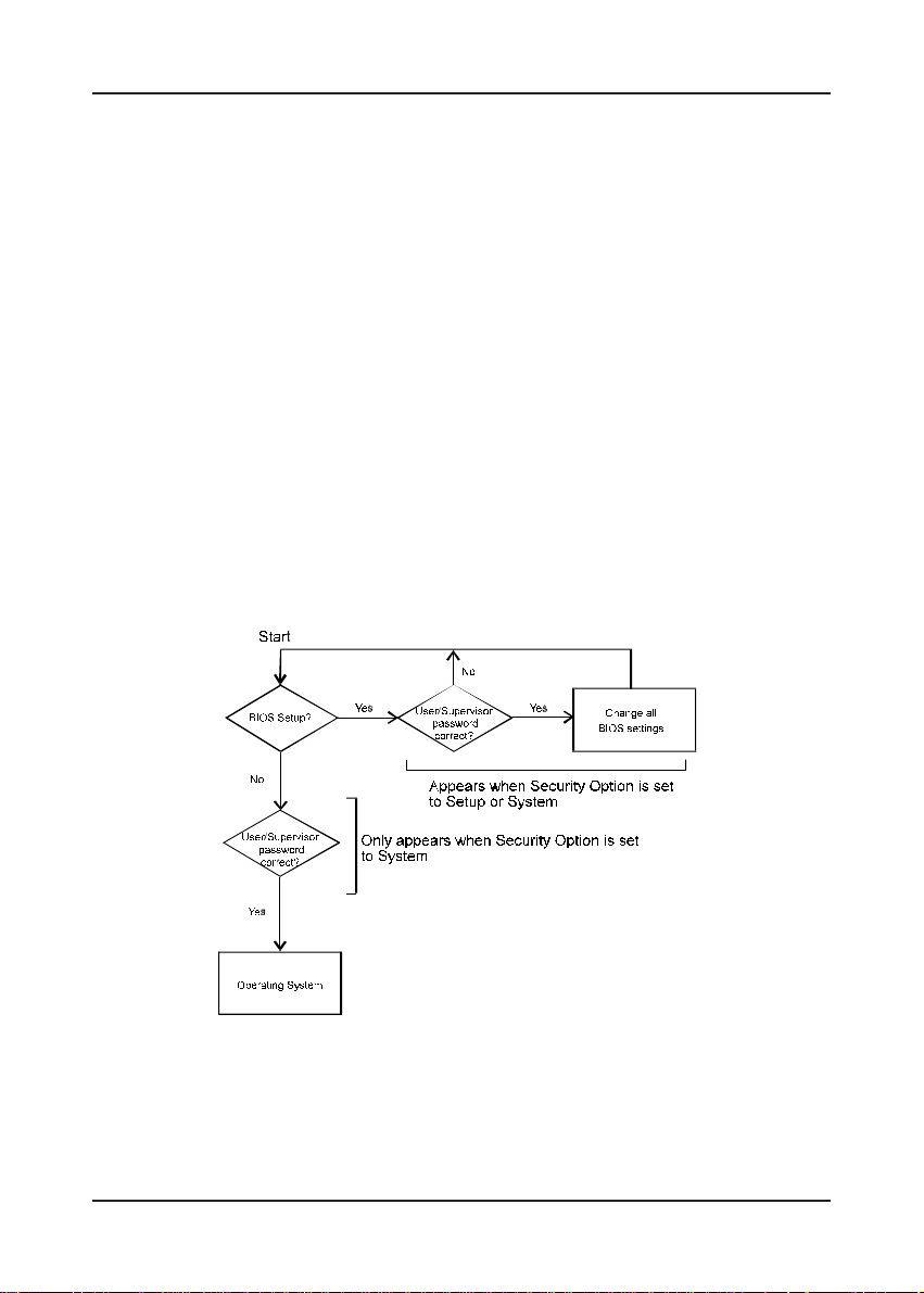
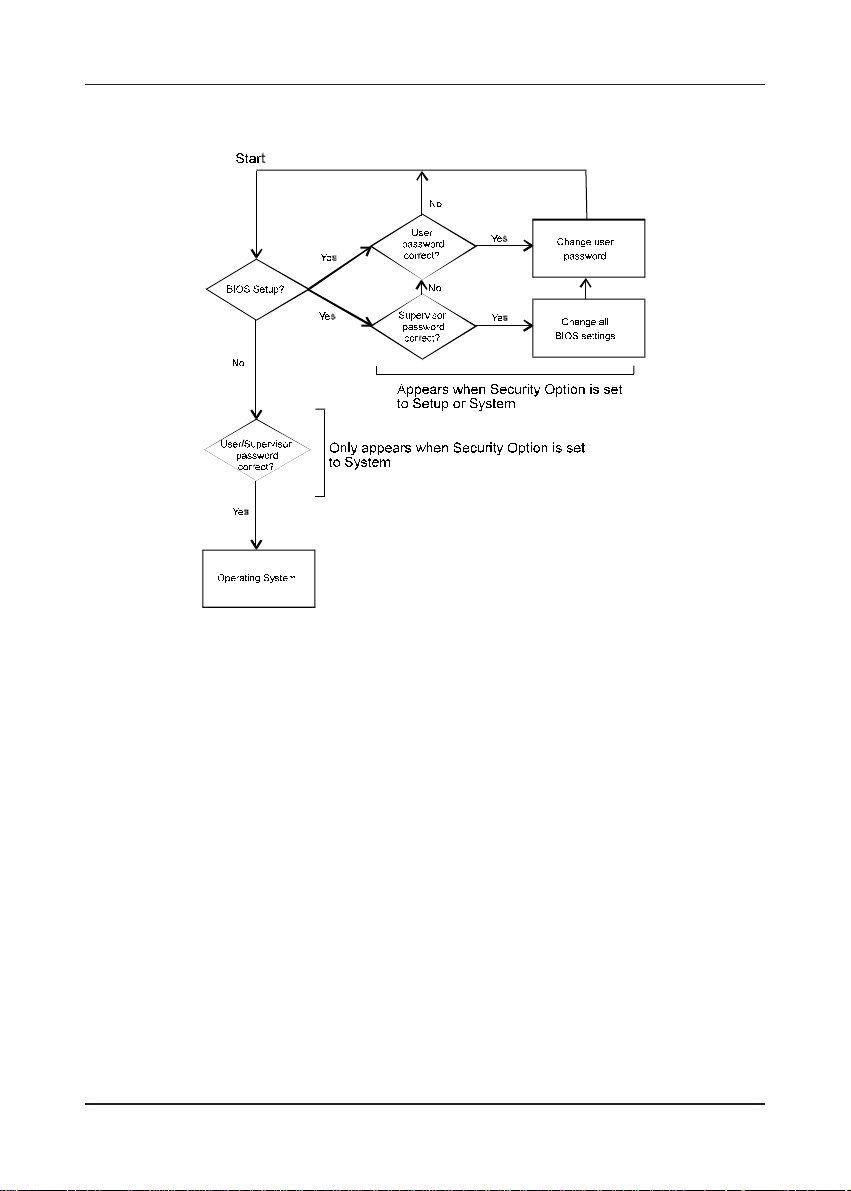
There are four different variables that control password settings. The first two are
located under the Security Option function in BIOS Features Setup Menu (Figure
3-3). When the Security Option function is set to Setup, a password is required to
enter BIOS and change BIOS settings. When the Securitiy Option function is set
to System, a password is required to to enter both BIOS and the the computer's
operating system (for example Windows 95) found on the boot drive. This is shown
in Figures 3-9 and 3-10.
The third and fourth variables are user password and supervisor password selected
in BIOS (Figure 3-1). The main purpose of separating user and supervisor is to allow
only the supervisor to have control over the settings in BIOS. The user, on the other
hand, is only allowed to access the computer's operating system and change the user
passorword in BIOS (See Figure 3-10 below). Note that when there is no supervisor
password set, the user password controls access to all BIOS settings (See Figure
3-9 below).
A. Set Either Supervisor Password or User Password
Figure 3-9 Set Either Supervisor or User Password
37
Page 42
Chapter 3
B. Set Both Supervisor Password and User Password
38
Figure 3-10 Set Both Supervisor and User Password
Page 43

Award BIOS Setup Program
3-9 IDE HDD Auto Detection
This utility can automatically detect IDE hard disk type and parameters. The detection
process take about 5 seconds for each physical drive. After the utility detects the
disk drive, type Y and press [Enter] to automatically load the parameters in the Hard
Disk section of the Standard CMOS Setup menu. Otherwise, leave the option set
at N and press [Enter] or the [Esc] key to skip the detected drive. After detecting
your hard drive(s), return to the Standard CMOS menu to check your settings.
ROM PCI / ISA BIOS (2A5LEC39)
CMOS SETUP UTILITY
AWARD SOFTWARE, INC.
HARD DISKS TYPE SIZE CYLS HEAD PRECOMP LANDZ SECTOR MODE
Primary Master:
Select Primary Master Option (N=Skip) : N
OPTIONS SIZE CYLS HEAD PRECOMP LANDZ SECTOR MODE
2 (Y) 547 530 32 0 1059 63 LB A
1 547 1060 1 6 65535 1059 63 NORMAL
3 547 530 32 65535 1059 63 LARGE
Note: Some OSes (like SCO-UNIX) must use "NORMAL" for installation
ESC: Skip
Figure 3-11 IDE HDD Auto Detection Screen
3-10 Save and Exit Setup
If you select this and type Y (for yes) followed by the [Enter] key, the values
entered in the setup utilities will be recorded in the CMOS memory of the BIOS
chip.
3-11 Exit Without Saving
Selecting this option and pressing Y followed by the [Enter] key lets you exit the
Setup program without recording any new values or changing old ones.
39
Page 44

Chapter 3
- Memo
40
Page 45

Mainboard Software
Chapter 4
Mainboard Software Guide
In the following installation instructions, drive D:\ is assumed to be your CDROM disk drive.
4-1 VIA ACPI Patch for Win95
Windows 95 software was written before the VIA chipset on your mainboard was
designed and manufactured. Thus, the newer chipset contains information not
recognized by Windows 95. This problem results in an abnormal appearance of
question and/or exclamation marks in the Windows 95 Device Manager window.
You can verify this problem by looking at the Windows 95 Device Manager
window via the following pathway: Start/Settings/Control Panel/System/Device
Manager. The chipset manufacturer has written a Patch file that allows Windows
95 to identify all the components of the chipset. Installing this Patch file will
remove question and/or exclamation marks. However, since the performance of
Windows 95 was not compromised by the lack of this patch, there will be no
increase in Windows 95 performance after installation.
To use the auto-install feature to install the VIA ACPI Patch, do the following:
1. Start Windows 95.
2. Insert the CD-ROM disk that came with your mainboard into your CD-ROM
drive. The CD-ROM will autorun and a software installation window will
appear.
3. Click on the VIA ACPI Patch for Win95 button and follow instructions on the
screen to complete the software installation.
4. Restart the computer.
To install the VIA ACPI Patch manually, click on the Setup application file located
at D:\Viapatch\Setup.exe in Windows Explorer. Be sure to restart your computer
after installation.
4-2 VIA IDE Bus Master Drivers for Win95 and WinNT
IDE Bus Mastering drivers are included for best IDE performance. To use the
auto-install feature to install the IDE driver, do the following:
41
Page 46

Chapter 4
1. Start Windows 95.
2. Insert the CD-ROM disk that came with your mainboard into your CD-ROM
drive. The CD-ROM will autorun and a software installation window will
appear.
3. Click on the VIA IDE Bus Master Drivers button and follow instructions on
the screen to complete the software installation.
4. Restart the computer.
To install the IDE driver manually, click on the Setup application file located at
D:\Viaide\Setup.exe in Windows Explorer. The Setup program will determine if
you are using Windows 95 or Windows NT 4.0. Be sure to restart your computer
after installation.
4-3 VIA AGP VxD Drivers for Win95
VxD drivers are used in the allocation of memory resources between your AGP
card and your system's main memory. The installation of this software is
necessary for the proper functioning of your AGP VGA port. You must also
comply with the following conditions to obtain proper functioning of your AGP
port.
1. Use Windows 95 version OSR2.1 (OEM Service Release 2 plus USB
supplement). If you have Windows 95 OSR2 and you would like to update to
the USB supplement, obtain and install USBSUPP.EXE from Microsoft which
also includes the new memory manager (VMM32.VxD) needed for the AGP
DIME (Direct Memory Execute) feature.
2. Install DirectX 5.0 from Microsoft. DirectX 5.0 is the first DirectX version
that supports AGP's DIME and should be supplied by your AGP VGA card
manufacturer.
3. Install the AGP VGA Driver supplied by your AGP VGA card manufacturer.
To use the auto-install feature to install the VxD drivers, do the following:
1. Start Windows 95.
2. Insert the CD-ROM disk that came with your mainboard into your CD-ROM
drive. The CD-ROM will autorun and a software installation window will
appear.
3. Click on the VIA AGP VxD Drivers for Win95 button and follow instructions
on the screen to complete the software installation.
4. Restart the computer.
To install the VxD drivers manually, click on the Setup application file located at
D:\ViaVxD\Setup.exe in Windows Explorer. Be sure to restart your computer
after installation.
42
Page 47

Mainboard Software
4-4 Trend Antivirus Utility for Win95
Your CD-ROM contains PC-cillin, software used in detecting and cleaning viruses
from your computer. The readme.txt file located at D:\Pccillin\readme.txt
contains important information regarding the use of this software. To use the
auto-install feature to install PC-cillin, do the following:
1. Start Windows 95.
2. Insert the CD-ROM disk that came with your mainboard into your CD-ROM
drive. The CD-ROM will autorun and a software installation window will
appear.
3. Click on the Trend Antivirus Utility button and then choose a language.
4. Follow instructions on the screen to complete the software installation.
5. Restart the computer.
To install PC-cillin manually, click on the Setup application file located at
D:\Pccillin\(choose a language)\Setup.exe in Windows Explorer. Be sure to
restart your computer after installation.
4-5 Shepherd System Monitoring Software for Win95 OR
Genesys System Monitoring Software for Win95/WinNT
Depending on the type of packaging your system assembler ordered, you
will either receive Shepherd or Genesys System monitoring software.
Shepherd or Genesys, in combination with this mainboard's system monitoring
hardware, detects the rpm speed of both system and CPU fans, CPU temperature,
and the input and output of one on-board voltage(Genesys detects four on-board
voltages). If something goes wrong in your system, an alarm will sound and
display appropriate error data in an error output window. To use the auto-install
feature to install Shepherd, do the following:
1. Start Windows 95.
2. Insert the CD-ROM disk that came with your mainboard into your CD-ROM
drive. The CD-ROM will autorun and a software installation window will
appear.
3. Click on the Shepherd or System Monitor button.
4. Follow instructions on the screen to complete the software installation.
5. Restart the computer.
To install Shepherd manually, click on the Setup application file located at
D:\Shepherd\Setup.exe in Windows Explorer. For Genesys, click on the Setup
file for Genesys at D:\SysMon\Win95\Setup.exe or D:\SysMon\WinNT\Setup.exe.
Be sure to restart your computer after installation.
43
Page 48

Chapter 4
4-6 Award Flash Utility
It is highly recommended that you make a back up copy of the old BIOS
before installing the new version. In case the new version is not
functional, you may reinstall the old copy. See the next page for backup
instructions.
Your system is equipped with a Flash ROM which allows users to update the BIOS
to a newer version without changing components. We suggest that you update
BIOS using the following method--Obtain an updated version of BIOS from your
mainboard vendor. In the Windows 95 or DOS environments, copy the following
two programs to a formatted, bootable disk.
A) The new version of BIOS (this is a ".bin" file).
B) The Award Flash Utility located in the enclosed CD-ROM's root directory
D:\FLASH\AWDFLASH.EXE (assume D is CD-ROM Drive).
Follow the instructions below to complete the BIOS upgrade.
1. Insert the disk prepared above into the floppy disk drive.
2. Type "A(or B):\AWDFLASH" at DOS command line and press
[Enter] key.
44
3. You will see the setup screen as shown below.
4. Please key in BIOS file name. (The filename will be released from
your dealer when a new up-dated BIOS is released).
FLASH MEMORY WRITER V5.35a
Copyright (C) 1996, Award Software, Inc.
For VP3-568B-8661-2A5LEC39C DATE: 03/04/98
Flash Type - SST 28EE010 & 28EE011 /5V
File Name to Program:
Error Message:
Page 49

Mainboard Software
5. If you don't want to save the previous BIOS data to the diskette, please
key in [N].
FLASH MEMORY WRITER V5.35a
Copyright (C) 1996, Award Software, Inc.
For VP3-568B-8661-2A5LEC39C DATE: 03/04/98
Flash Type - SST 28EE010 & 28EE011 /5V
File Name to Program 5AGM.BIN
Error Message: Do You Want To Save BIOS (Y/N)
6. If you want to save the previous BIOS data to the diskette, please
key in [Y].
FLASH MEMORY WRITER V5.35a
Copyright (C) 1996, Award Software, Inc.
For VP3-568B-8661-2A5LEC39C DATE: 03/04/98
Flash Type - SST 28EE010 & 28EE011 /5V
File Name to Program 5AGM.BIN
Now Backup System BIOS to BIOS. Old file!
Error Message: Please Wait !
7. Type [Y], then you will start the programming.
FLASH MEMORY WRITER V5.35a
Copyright (C) 1996, Award Software, Inc.
For VP3-568B-8661-2A5LEC39C DATE: 03/04/98
Flash Type - SST 28EE010 & 28EE011 /5V
File Name to Program 5AGM.BIN
Error Message: Are You Sure To Program (Y/N)
45
Page 50
Chapter 4
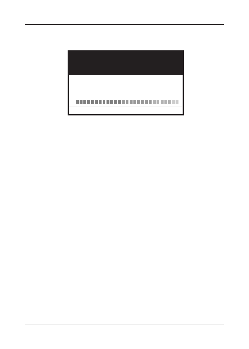
8. After the programming finishes, remove the floppy disk and reset
the computer.
FLASH MEMORY WRITER V5.35a
Copyright (C) 1996, Award Software, Inc.
For VP3-568B-8661-2A5LEC39C DATE: 03/04/98
Flash Type - SST 28EE010 & 28EE011 /5V
File Name ot Program 5AGM.BIN
Programming Flash memory - OK
Error Message: Please Power Off Or Reset System !
4-7 Award DMI Configuration Utility
DMI (Desktop Management Interface) is a new method of managing computers in an enterprise network. The main component of DMI is the
MIFD(Management Information Format database). This database contains all the
information about the computing system and its components. Using DMI, a system
administrator can obtain the types, capabilities, operational status, installation data
and other information about the system components.
We support DMI features in BIOS and provide a DMI utility to maintain a
MIFD file.
The system BIOS uses the same technology implemented for plug and play to
allow dynamic real-time update system information and store those collected
information (e.g. CPU type and speed, Bus frequency , memory size and speed) block
in the motherboard's Flash EPROM.
We also provide a friendly DMI utility (DMICFG.EXE) to allow the system
integrator or end user to place necessary information in MIFD such as the serial
number on the motherboard, add-on cards, monitor, etc. This information is not
detected by the system BIOS and has to be manually input through the DMI
utility.
46
Page 51

Mainboard Software
The DMICFG.EXE(DMI Configuration Utility for modifying/reviewing the MIFD)
contained in Drivers Disk that comes with your mainboard.
Please remove (or remark) any installed Memory Management Utility
(such as EMM386.EXE, QEMM.EXE...,etc.) in the CONFIG.SYS files
before running this utility.
Run DMICFG.EXE at D\:DMI\DMICFG and the following screen will prompt:
Award DMI Configuration Utility v1.08u, Copyright Award Software Inc. 1996
[Edit DMI] [Add DMI] [Load DMI FILE] [Save DMI FILE]
BIOS == Display Component ===
System
Base Board
Enclosure/Chassis Type : BIOS Information
Processor Handle : 0000
Memory Controller Vendor Name : Award software International, Inc.
Memory Module BIOS Version : 4.51 PG
Memory Module BIOS Starting Address Segment : E000
Memory Module BIOS Build Date : 03/04/98
Memory Module BIOS Characteristics : Press [Enter] for detail
Memory Module Size of BIOS ROM : 0128K
Memory Module
Cache
Cache
Port Connector
Port Connector
Port Connector
Port Connector
Port Connector
Port Connector
-Move cursor Enter-Accept DEL-Delete ESC-Abort&Exit
Use the (left-right) cursor to move the top menu items and the (up-down)
cursor to move between the left hand menu items. The bottom of the screen will
show the available keys for each screen. Press [Enter] at the menu item to enter
the right hand screen for editing.
If you have made any changes, press [F10] to ensure the data keep in Flash
ROM.
47
Page 52

Chapter 4
- Memo
48
Page 53

Introduction
Appendix I
On Board I/O Addresses & IRQ Maps
System Resource IRQ I/O Address
1. Timer IRQ0 040, 043
2. Keyboard IRQ1 060, 064
3. Programmable INT IRQ2 0020, 0021,
00A0, 00A1
4. COM2(B) IRQ3 2F8, 2FF
5. COM1(A) IRQ4 3F8, 3FF
6. Floppy IRQ6 3F0, 3F7
7. LPT1 IRQ7 378, 37F
8. Real Time Clock IRQ8 070, 071
9. PS/2 Mouse IR Q12 060, 064
10.Math coprocessor IRQ 13 0F0, 0FF
11.IDE 1 IR Q1 4 1F0, 1F7
12.IDE 2 IR Q1 5 170, 177
@@
@
IRQ 5, 9, 10 and 11 are available for interface cards.
@@
43
Page 54

User's Manual
- Memo
44
Page 55
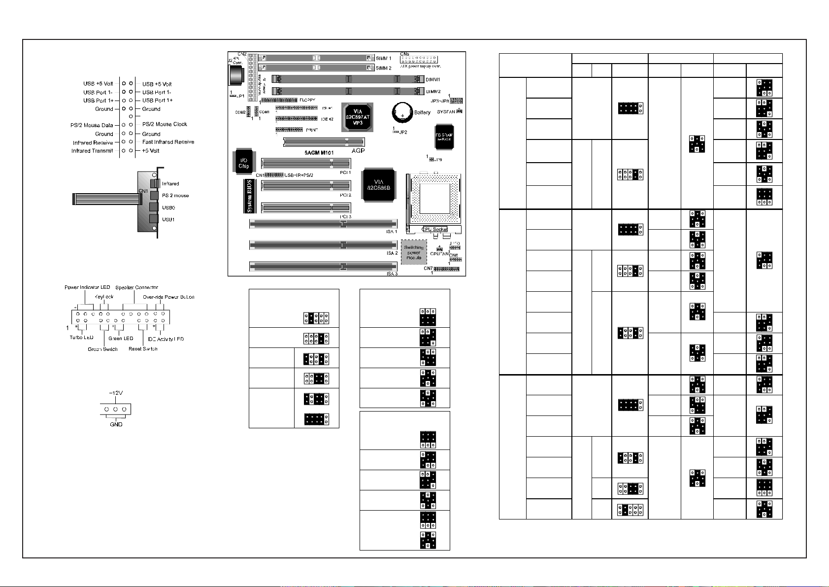
1998.02
Quick Connector and Jumper ReferenceQuick Connector and Jumper Reference
Quick Connector and Jumper Reference
Quick Connector and Jumper ReferenceQuick Connector and Jumper Reference
CN1: PS/2 mouse, USB, Infrared connector
with optional USB kit
CN6: FAN78 connector
CN7: Front Panel connector set
CPUFAN/SYSFAN: CPU/System cooling
fan connector
JP1: AT/ATX power supply jumper
1~2: AT power
2~3: ATX power
JP2: Clear CMOS data jumper
1~2: Normal(default)
2~3: Clear CMOS data
JP9: Reserved for factory
V.1
22-A
Vcore JP10
2.2V
2.8V
2.9V
3.2V
3.3V
3.5V
1
1
1
1
1
1
System Freq. JP3~JP5
50MHz
55MHz
60MHz
66MHz
75MHz
Freq. Ratio JP6~JP8
x 1.5
x 2
x 2.5
x 3
x 3.5
x 4
1
1
1
1
1
1
1
1
1
1
1
CPU-type
P54C-133
P54C-166 x2.5
P54C-200 x3
Intel
Pentium w/MMX
@166MHz
Pentium w/MMX
@200MHz
Pentium w/MMX
@233MHz
6x86-PR166
@133MHz
6x86-PR200
@150MHz
6x86L-PR166
@133MHz
6x86L-PR200
Cyrix
/IBM
AMD
@150MHz
6x86MX-PR166
6x86MX-PR200 x2.5
6x86MX-PR200
6x86MX-PR233 x2.5
K5-PR133
@100MHz
K5-PR150
@105MHz
K5-PR166
@116.7MHz
K6/166
K6/200 x3
K6/233 3.2 x3.5
K6/266 2.2 x4
CPU Power Voltage System freq. Freq. ratio
Core
I/O Vcc
3.5
3.3 2.8
3.5
3.3
Vcc
2.8
JP10 MHz
1
1
1
66
66
75
66
75
66
1
2.9
75
66 x2
1
3.5
60
66
1
2.9
3.3
1
66
1
JP3~JP5 Speed rate
x2
1
x2.5
x3
x3.5
1
1
1
x2
1
1
1
x2
1
1
1
x2.5
x2.5
1
JP6~JP8
1
1
1
1
1
1
1
1
1
1
1
1
1
1
1
586AGM0.1
Page 56

Page 57
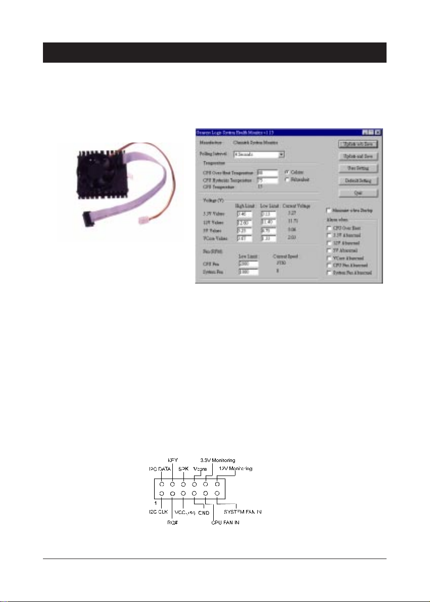
Appendix II
FAN78-
The FAN78 upgrade kit provides a PC self-dialogistic capability called the SMART
(System Monitoring and Alerting) technology.
Features
- Detects four on-board voltages (CPU Core Voltage, 3.3V, 5V, 12V)
- Two fan speed sensing
- One precise CPU temperature sensor and one chassis temperature sensor
- Four types of speaker-driver signal output
- Supports system monitor software and drivers for LDCMTM utility V3.1
- EISCA v1.0 compliant
SMART
FAN78
Technology Upgrade Kit
System Monitor Software for Win95
FAN78 Connector
45
Page 58

- Memo
46
 Loading...