

Page 1

.
© 1999-2003 Centrality Commnications, Inc.
2520 Mission College Blvd. Suite #103, Santa Clara, CA 95054
Atlas™
Programming Guide
Preliminary Revision 0.6, April 2003
Page 2

**Preliminary and Confidential under NDA, DO NOT DISTRIBUTE
Atlas™ Programming Guide **Preliminary and Confidential under NDA, DO NOT DISTRIBUTE
- 1 -
Table of Contents
1 Introduction ..........................................................................................................................................7
1.1 Documentation Conventions ........................................................................................................ 7
1.2 Referenced Documents................................................................................................................ 8
1.3 Architectural Overview.................................................................................................................. 9
1.4 Key Features .............................................................................................................................. 11
2 RISC Subsystem................................................................................................................................12
2.1 Operation Overview.................................................................................................................... 12
2.2 RISC Address Mapping.............................................................................................................. 12
2.3 Boot-up Control .......................................................................................................................... 14
2.4 Wait State Control ...................................................................................................................... 15
2.5 Write Pulse Control..................................................................................................................... 16
2.6 Timeout Control .......................................................................................................................... 17
3 DSP Subsystem.................................................................................................................................18
3.1 Operation Overview.................................................................................................................... 18
3.2 DSP Memory Address Mapping ................................................................................................. 19
3.3 DMA Operation........................................................................................................................... 20
3.3.1 Setting Memory Status........................................................................................................ 20
3.3.2 Starting DMA Transfer......................................................................................................... 20
3.3.3 Endian Mode for DMA ......................................................................................................... 21
3.3.4 Byte Select Mode ................................................................................................................21
3.4 Controlling Peripherals ............................................................................................................... 23
3.5 DSP and RISC Cooperation....................................................................................................... 24
3.5.1 RISC Control DSP by Interrupt ........................................................................................... 24
3.5.2 Data exchange between the RISC and the DSP ................................................................ 26
3.6 Differences between the DSP and ADI’s ADSP2181................................................................. 27
3.6.1 Memory ............................................................................................................................... 27
3.6.2 Instructions .......................................................................................................................... 27
3.6.3 Biased-rounding mode ........................................................................................................ 27
3.6.4 Non-memory mapped registers........................................................................................... 27
3.6.5 Memory mapped registers................................................................................................... 27
3.6.6 Critical path limitation .......................................................................................................... 27
4 Dynamic Memory Interface................................................................................................................29
4.1 Operation Overview.................................................................................................................... 29
4.2 Pin Sharing ................................................................................................................................. 30
4.3 Normal Operation ....................................................................................................................... 31
4.4 Wake-up Operation .................................................................................................................... 33
4.5 Clock Switching Operation ......................................................................................................... 34
4.6 Self-refresh Mode ....................................................................................................................... 35
5 Static memory Interface.....................................................................................................................36
5.1 Operation Overview.................................................................................................................... 36
5.2 Instruction Access Mode ............................................................................................................ 36
5.3 Direct Access Mode.................................................................................................................... 38
5.4 DMA Access Mode ..................................................................................................................... 39
5.4.1 DMA read ............................................................................................................................ 39
5.4.2 DMA write............................................................................................................................ 40
6 Clocks and Power Manager...............................................................................................................47
6.1 Operation Overview.................................................................................................................... 47
6.2 Change Clock Source................................................................................................................. 48
6.3 Change Clock Ratio.................................................................................................................... 49
6.3.1 Change the System and I/O Clock Ratio ............................................................................ 49
6.3.2 Change the External Memory Clock Ratio.......................................................................... 49
6.4 Change PLL Frequency.............................................................................................................. 51
6.5 Power Mode ............................................................................................................................... 52
Page 3

**Preliminary and Confidential under NDA, DO NOT DISTRIBUTE
Atlas™ Programming Guide **Preliminary and Confidential under NDA, DO NOT DISTRIBUTE
- 2 -
6.5.1 Normal Mode....................................................................................................................... 52
6.5.2 Turbo Mode ......................................................................................................................... 52
6.5.3 Idle Mode............................................................................................................................. 52
6.5.4 Standby Mode ..................................................................................................................... 53
6.5.5 Sleep Mode ......................................................................................................................... 53
7 GPIO ..................................................................................................................................................55
7.1 Operation Overview.................................................................................................................... 55
7.2 Configure GPIO Pin Sharing ......................................................................................................56
7.3 Configure GPIO as Input ............................................................................................................ 57
7.4 Configure GPIO as Output ......................................................................................................... 58
7.5 Configure GPIO as Open-Drain ................................................................................................. 59
7.6 Configure GPIO as Wake-up Source ......................................................................................... 60
7.7 Configure GPIO to be Accessed by DSP................................................................................... 61
8 Resource Sharing Controller .............................................................................................................62
8.1 Operation Overview.................................................................................................................... 62
8.2 DMA Channel Sharing................................................................................................................ 63
8.3 External Pin Multiplex................................................................................................................. 64
9 DMA Controller ..................................................................................................................................66
9.1 Operation Overview.................................................................................................................... 66
9.2 Initialization................................................................................................................................. 67
9.3 DMA Interrupt Handling .............................................................................................................. 69
9.4 Single and Burst DMA ................................................................................................................ 70
9.5 1-D and 2-D DMA ....................................................................................................................... 71
9.6 Loop DMA................................................................................................................................... 73
9.7 DSP Control of DMA................................................................................................................... 76
10 PCMCIA Interface..............................................................................................................................77
10.1 Operation Overview ................................................................................................................ 77
10.2 Pin-mux Programming ............................................................................................................ 78
10.3 M6730 Register Programming................................................................................................ 79
10.4 Power Logic Register Programming ....................................................................................... 81
10.5 Memory Window Configuration............................................................................................... 82
10.6 I/O Window Configuration....................................................................................................... 83
10.7 Timing Control......................................................................................................................... 84
10.8 Management Interrupt Operation............................................................................................ 84
10.9 Card Interrupt Operation......................................................................................................... 86
10.10 Socket Initialization Sequence................................................................................................ 87
11 Extension port ....................................................................................................................................88
11.1 Operation Overview ................................................................................................................ 88
11.2 Pin-mux Programming ............................................................................................................ 89
11.3 Timing Register Programming ................................................................................................ 90
11.4 Fixed Latency Access ............................................................................................................. 91
11.5 Variable Latency Access.........................................................................................................92
11.6 DSP Access ............................................................................................................................ 93
12 Universal Serial Port ..........................................................................................................................94
12.1 Operation Overview ................................................................................................................ 94
12.2 USP Reset and Power up ....................................................................................................... 95
12.3 USP Initialization..................................................................................................................... 96
12.3.1 USP Work Mode Initialization.............................................................................................. 96
12.3.2 Sample Code of USP Initialization ...................................................................................... 99
12.4 USP Transmitting Operation................................................................................................. 105
12.4.1 I/O Mode Transmit by Interrupt ......................................................................................... 105
12.4.2 I/O Mode Transmit by Polling FIFO Status ....................................................................... 105
12.4.3 DMA Transmitting Mode.................................................................................................... 105
12.5 USP Receiving Operation ..................................................................................................... 107
12.5.1 I/O Mode Receiving by Interrupt ....................................................................................... 107
Page 4

**Preliminary and Confidential under NDA, DO NOT DISTRIBUTE
Atlas™ Programming Guide **Preliminary and Confidential under NDA, DO NOT DISTRIBUTE
- 3 -
12.5.2 I/O Mode Receiving by Polling FIFO Status...................................................................... 107
12.5.3 DMA Recieving Mode........................................................................................................ 108
12.6 Interralation of Transmitting and Receiving .......................................................................... 109
12.6.1 Independent Operation for Transmitting and Receiving ................................................... 109
12.6.2 concurrent Operation for Transmitting and Receiving ...................................................... 109
12.6.3 Alternate Operation for Transmitting and Receiving......................................................... 109
12.7 Pin I/O Mode Operations ...................................................................................................... 109
12.8 USP Reconfiguration ............................................................................................................ 111
12.9 SIB Initialization .................................................................................................................... 112
12.10 SIB Operations...................................................................................................................... 114
12.10.1 Register Writing ............................................................................................................. 114
12.10.2 Register Reading ........................................................................................................... 114
12.10.3 Audio Data Transfer....................................................................................................... 114
12.10.4 Telecom Data Transfer.................................................................................................. 115
13 Audio CODEC Interface...................................................................................................................116
13.1 Operation Overview ..............................................................................................................116
13.2 AudioCODEC Controller Initialization ................................................................................... 117
13.3 AC’97 CODEC Configuration................................................................................................ 118
13.4 I2S CODEC Configuration .................................................................................................... 122
14 Camera Interface .............................................................................................................................124
14.1 Operation Overview ..............................................................................................................124
14.2 Initialize Operations .............................................................................................................. 125
14.2.1 Initialize Camera Interface ................................................................................................ 125
14.2.2 Camera Interrupt Operation .............................................................................................. 125
14.3 DMA Operations ................................................................................................................... 127
14.3.1 Initialize DMA Interface ..................................................................................................... 127
14.3.2 DMA Interrupt Operation ................................................................................................... 127
14.3.3 DMA operation .................................................................................................................. 128
14.4 Sensor Operations................................................................................................................ 129
14.4.1 Initialize Sensor Control Module ....................................................................................... 129
14.4.2 Sensor Clock Operation .................................................................................................... 129
14.4.3 Capture Image Operation.................................................................................................. 129
14.4.4 Slave Mode Operation....................................................................................................... 130
14.4.5 Pixel Data Shift Operation................................................................................................. 131
14.4.6 Inverse Control Operation ................................................................................................. 132
14.4.7 Sample Pixel Clock Operation .......................................................................................... 132
14.4.8 Master Mode Operation..................................................................................................... 133
14.5 I2C Master Operations.......................................................................................................... 135
14.5.1 Initialize Unit ...................................................................................................................... 135
14.5.2 Write n Bytes to External Device....................................................................................... 135
14.5.3 Read n Bytes from External Device .................................................................................. 136
14.6 I2C Slave Operations............................................................................................................137
14.6.1 Initialize Unit ...................................................................................................................... 137
14.6.2 Normal Operation .............................................................................................................. 137
14.7 Quick Reference ................................................................................................................... 138
15 USB 1.1 Device Interface ................................................................................................................139
15.1 Operation Overview ..............................................................................................................139
15.2 Initialization ........................................................................................................................... 141
15.3 Control Transfer .................................................................................................................... 143
15.4 I/O Operation ........................................................................................................................ 145
15.5 DMA Operation ..................................................................................................................... 147
15.6 Quick Reference ................................................................................................................... 149
16 Host Port Interface ...........................................................................................................................150
16.1 Operation Overview ..............................................................................................................150
16.2 Address Mapping .................................................................................................................. 151
Page 5

**Preliminary and Confidential under NDA, DO NOT DISTRIBUTE
Atlas™ Programming Guide **Preliminary and Confidential under NDA, DO NOT DISTRIBUTE
- 4 -
16.3 Initialization ........................................................................................................................... 152
16.4 I/O & DMA Operation............................................................................................................ 155
16.5 Handshaking with Host ......................................................................................................... 157
17 Secure Disk (SD) / Multi-Media Card Interface (MMC) ...................................................................158
17.1 Operation Overview ..............................................................................................................158
17.2 Internal Regsiter Programming............................................................................................. 159
17.3 I/O Operation ........................................................................................................................ 160
17.4 DMA Operation ..................................................................................................................... 161
17.5 Initialization ........................................................................................................................... 162
17.6 No Data Command/Response Transaction .......................................................................... 163
17.7 Single Block Operation ......................................................................................................... 164
17.7.1 Single Block Write ............................................................................................................. 164
17.7.2 Single Block Read ............................................................................................................. 164
17.8 Multiple Block Operation....................................................................................................... 165
17.8.1 Multiple Block Write........................................................................................................... 165
17.8.2 Multiple Block Read........................................................................................................... 165
17.8.3 Multiple Block Write Using Number Blocks....................................................................... 166
17.8.4 Multiple Block Read Using number Blocks ....................................................................... 166
18 Nand Flash Memory Interface .........................................................................................................167
18.1 Operation Overview ..............................................................................................................167
18.2 Initialization ........................................................................................................................... 167
18.3 I/O Operation ........................................................................................................................ 167
18.3.1 IO Read ............................................................................................................................. 167
18.3.2 IO Write ............................................................................................................................. 168
18.4 DMA Operation ..................................................................................................................... 168
18.5 DMA read example ............................................................................................................... 169
18.6 DMA write example...............................................................................................................169
18.7 NAND Boot-loader ................................................................................................................170
18.7.1 ARM Init Process............................................................................................................... 171
18.7.2 Flash Controller’s global register init process ................................................................... 172
18.7.3 Read Device ID ................................................................................................................. 172
18.7.4 Search File “NK.BIN”......................................................................................................... 172
18.7.5 Read “NK.BIN” and Parse It.............................................................................................. 172
18.8 Special Notes........................................................................................................................ 173
19 LCD Controller Interface ..................................................................................................................174
19.1 Operation Overview ..............................................................................................................174
19.2 Initialization ........................................................................................................................... 174
19.3 DMA Operation ..................................................................................................................... 176
19.4 Configuration Comparison for Different Mode ...................................................................... 177
19.5 Palette................................................................................................................................... 178
19.5.1 Color Palette...................................................................................................................... 178
19.5.2 Grey Palette of FRC Sequence......................................................................................... 178
19.6 Special Register Configuration ............................................................................................. 179
19.6.1 Pixel Clock Divider ............................................................................................................ 179
19.6.2 FIFO Request Watermark Control .................................................................................... 179
19.7 Power Sequence / Back Light Control for LCD Displays...................................................... 179
20 Revision History ...............................................................................................................................180
Page 6

**Preliminary and Confidential under NDA, DO NOT DISTRIBUTE
Atlas™ Programming Guide **Preliminary and Confidential under NDA, DO NOT DISTRIBUTE
- 5 -
List of Figures
Figure 1. Atlas™ Block Diagram .......................................................................................................... 9
Figure 2. DSP Byte Select Mode........................................................................................................ 22
Figure 3. Data Mapping in 8-bit External Data Bus............................................................................ 37
Figure 4. Data Mapping in 16-bit External Data Bus.......................................................................... 37
Figure 5. Static Memory Interface Simple WriteTiming...................................................................... 41
Figure 6. Static Memory Interface Fixed Sequence WriteTiming....................................................... 43
Figure 7. Static Memory Interface Fixed Sequence WriteTiming....................................................... 45
Figure 8. Atlas™ Pin Multiplex Diagram............................................................................................. 64
Figure 9. 2-D DMA.............................................................................................................................. 71
Figure 10. 2-D DMA Wrap Around (X-Length > Width)........................................................................ 72
Figure 11. Loop-mode DMA ................................................................................................................. 73
Figure 12. NAND Boot Flow Diagram................................................................................................. 171
Page 7

**Preliminary and Confidential under NDA, DO NOT DISTRIBUTE
Atlas™ Programming Guide **Preliminary and Confidential under NDA, DO NOT DISTRIBUTE
- 6 -
List of Tables
Table 1. Reference Documents .............................................................................................................. 8
Table 3. DSP memory address mapping.............................................................................................. 19
Table 4. DSP memory usage guide...................................................................................................... 20
Table 5. DSP peripheral registers address mapping ............................................................................ 23
Table 6. Staitic Memory Chip Select Mapping...................................................................................... 36
Table 7. Staitic Memory Chip Select Mapping...................................................................................... 39
Table 8. Atlas™ DMA Channel Multiplex.............................................................................................. 63
Table 9. Atlas™ Pin Multiplex ............................................................................................................... 64
Table 10. Pixel Shift Number vs DMA Register Setting .................................................................... 138
Table 11. USB Device Endpoint Configuration ................................................................................. 149
Table 12. Differences between Master and Slave Mode .................................................................. 178
Table 13. FRC Sequence Table Example......................................................................................... 178
Page 8

**Preliminary and Confidential under NDA, DO NOT DISTRIBUTE
Atlas™ Programming Guide **Preliminary and Confidential under NDA, DO NOT DISTRIBUTE
- 7 -
1 Introduction
This document detailed descriptions and examples of programming and developing using the Centrality
Communications’ Atlas™ Processor. It is intended for the use of Centrality customers, partners, and
other interested parties to gain a detailed understanding of Centrality’s technology and architecture for
design purposes. Detailed programming guide, flow chart, and sample code are contained in this
manual to provide the user with a solid background.
1.1 Documentation Conventions
• In some sections, the documentation is still being finalized. In this case, a “TBD” will be in its
place meaning“To Be Determined”.
• Important items to make note are in blue and bold: i.e. NOTE: when laying out the SDRAM
Traces …
• Register names will be in all capital letters with an underscore for spacing. Examples include:
INT_FIQ_PENDING
• Include common conventions and assumptions for MSB, LSB, high, low, enable, etc…
• In this document, we refer to the ARM922T core as either RISC, RISC core, or ARM core.
These all refer to same ARM922T core licensed from ARM®.
• Figure Labels are placed below the figure; wheras table labels are placed above the tables they
are referring to.
• When diagrams include memory addresses, these are with respect to a specific memory domain.
When a figure describes a memory address, it will either explicitly include the memory domain
(i.e. PCMCIA, NAND Flash, SD…) or it is safe to assume it belongs to the domain of the relevant
section.
• Binary Values: Often in the register definitions specific fields within a 32 bit register are assigned
values. These values are represented by the following notation: For example if a three bit field
has the value of “3”, then the representation would be 2’b011.
• Hexadecimal Values: There are two types of representation of hexadecimal values: such as
16’h55AA, or 0x55AA.
Page 9

**Preliminary and Confidential under NDA, DO NOT DISTRIBUTE
Atlas™ Programming Guide **Preliminary and Confidential under NDA, DO NOT DISTRIBUTE
- 8 -
1.2 Referenced Documents
The following documents can be obtained from Centrality Communications to enhance the supplement
of the Atlas™ Processor.
Table 1. Reference Documents
File Name Description
ARM922T.PDF
ARM922T processor core technical reference manual.
BlueApp.PDF
Mindtree Consulting Bluetooth Baseband Controller Application
Document
BlueArch.PDF
Mindtree Consulting Bluetooth Baseband Controller Architechture
Document
BlueImp.PDF
Mindtree Consulting Bluetooth Baseband Controller Implementation
Document
BlueVer.PDF
Mindtree Consulting Bluetooth Baseband Controller Verification
Document
I2C-Bus
Specification.PDF
The I
2
C Bus Specification version 2.1
M6730 Design
Document.PDF
Virtual IP Group M6730 – PCI to PC Card Host Adaptor Block Level
Design Document
M6730 Users Guide.PDF
Virtual IP Group M6730 PCI to PC Card Host Adapter User Guide
V9012S_PM User
Guide.PDF
Virtual IP Group V9012S_PM – USB Device Controller User Guide
Atlas_dev1.PDF
Centrality Communications Atlas™ Processor layout schematics
reference
Developer’s Manual
Lite.PDF
Centrality Communications Atlas™ Processor Developer’s Manual
(Lite)
Page 10
**Preliminary and Confidential under NDA, DO NOT DISTRIBUTE
Atlas™ Programming Guide **Preliminary and Confidential under NDA, DO NOT DISTRIBUTE
- 9 -
1.3 Architectural Overview
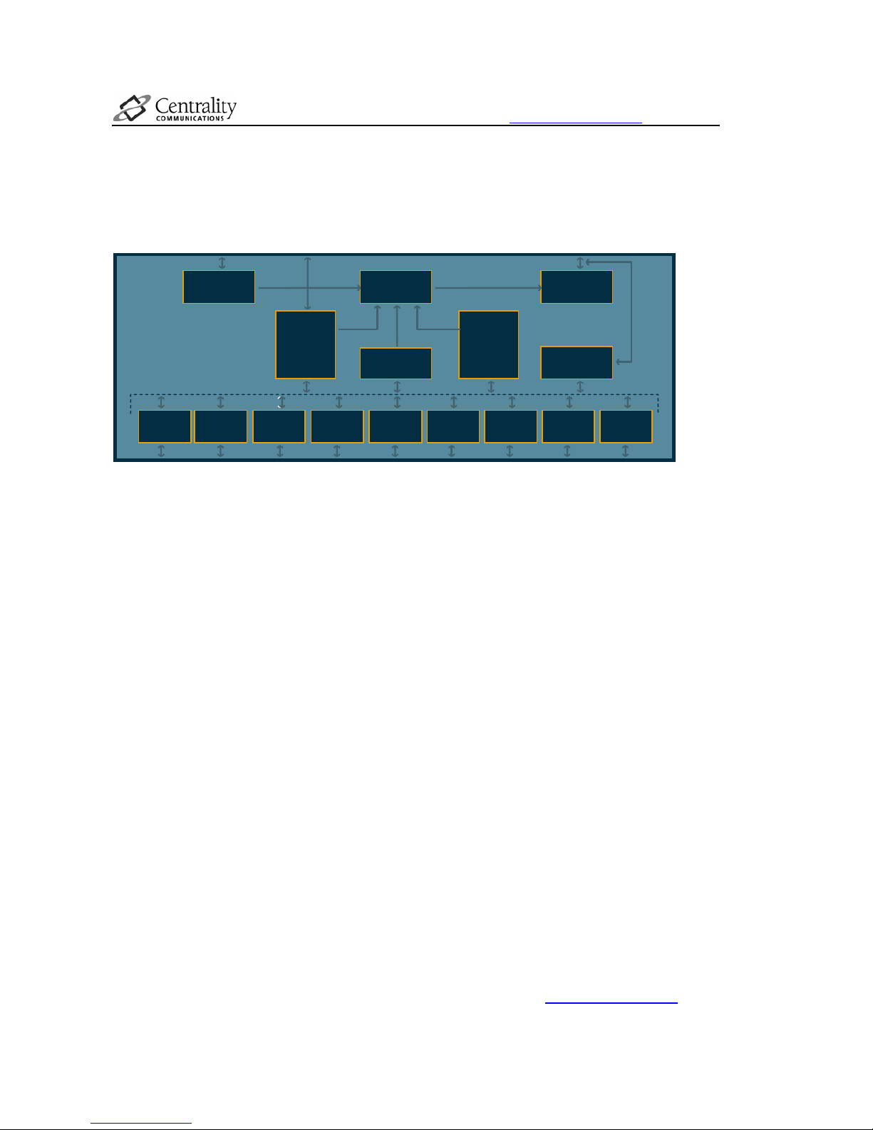
Figure 1 is the block diagram for Atlas™.
Figure 1. Atlas™ Block Diagram
• RISC Core
Atlas™ has an integrated ARM922T core with the AMBA ASB bus. The RISC acts as a controller, which
controls the other functional blocks via writing/reading memory-mapped registers. The RISC accesses
external memory via the memory bus and acts as a bus master.
• DSP Core
Most of the computation required for the multimedia and communication applications can be performed
in the Digital Signal Processor (DSP). The advantages of using a DSP include an increase in the
computation horsepower, effectiveness, and reduced memory footprint and bandwidth. The DSP
operates independent from the RISC processor and contains its own program and data memory space.
The DSP is also a bus master and can DMA data to/from external memory via the memory bus.
However, the DSP is controlled by the RISC processor through a shared register file. The RISC
processor can write commands into the register file and start/stop DSP programs. The DSP can also
write to the register file and transfer data/status to the RISC. The RISC and DSP can symbiotically
interrupt each other.
Both the RISC and the DSP can read/write to memory-mapped control registers to configure or read the
status of a peripheral block. This accesses takes place on two distinct buses, the RISC I/O Bus (RBUS)
and DSP I/O Bus (DBUS). Each block has a Control Register Interface to decode the register
accesses from the RISC and DSP and resolve any potential conflict. (Note: The RISC and the DSP can
simultaneously read/write two separate registers, as long as they are not in the same functional block).
• System Memory Bus
The system memory bus is a 32-bit high-performance, low-power bus. In the Atlas™ architecture, there
are 4 bus masters: RISC, DSP, I/O Bridge, and LCD Controller. The Bus Arbitrator arbitrates requests
of the four bus masters and directs the appropriate accesses to the single system memory bus slave –
the Memory Controller.
• Memory Controller
ARM
922T
DSP
Subsystem
System Memory
Bus Arbiter
Memory
Controller
ROM Interface
LCD Controller
I/O Bridge
NAND Flash
Smart Media
USB 1.1
Interface
SD/MMC
Interface
PCMCIA/CF
Host/Slave_
Extension
Port
Camera
Interface
Serial Ports
GPS
Baseband
Bluetooth
Baseband
SDRAM/SRAM
Flash/ROM
LCD Panel
LCD Driver
GPIOs
Keyboard
Bluetooth RF
GPS RF
IrDA, UART
CODEC, Tch-Scrn
CMOS/CCD
Sensor
NAND Flash
Smartmedia
USB Host
SD/MMC
Card
CF/PCMCIA
Host/Slave
Extension Chip
Page 11

**Preliminary and Confidential under NDA, DO NOT DISTRIBUTE
Atlas™ Programming Guide **Preliminary and Confidential under NDA, DO NOT DISTRIBUTE
- 10 -
The Memory Controller controls all access to external memory. The Memory Controller supports SDRAM
as the main memory for program and data storage during the chip’s normal operational mode. During
boot, the RISC processor will first transfer the code stored in Flash memory to the program space in the
SDRAM. After boot-up, the Flash memory can be considered as a peripheral device.
• Peripheral Subsystem
Atlas™ is a multi-functional platform, so it contains several peripheral interface blocks:
1) 16 channel GPS baseband
2) Bluetooth baseband
3) USB device interface
4) NAND Flash/Smart Media interface
5) CMOS/CCD sensor interface
6) NOR Flash/ROM interface
7) Universal Serial Ports
8) Audio CODEC interface
9) SD/MMC interface
10) LCD interface
All of these interface blocks have the same functionality: they each provide a means to transfer data
between Atlas™ and an external device. There are two types of transfer: I/O read/write and DMA. Some
blocks only support I/O read/write, such as the Bluetooth and GPS blocks. Some blocks support both I/O
read/write and DMA, such as the serial port, CMOS sensor, NAND Flash/Smartmedia, Flash/ROM,
SD/MMC and USB interface. Each peripheral has its own SRAM FIFO. The I/O read/write can be
executed by either the RISC or DSP, via the RBUS or DBUS respectively. The DMA can be executed
via the I/O memory bus. The peripheral blocks with DMA channel will connect to the I/O Bridge via the
I/O memory bus.
The I/O Bridge is responsible for the arbitration of the DMA requests from the peripherals. But it can only
grant the I/O memory bus to the peripheral when it's granted the system memory bus from the Bus
Arbiter.
Page 12

**Preliminary and Confidential under NDA, DO NOT DISTRIBUTE
Atlas™ Programming Guide **Preliminary and Confidential under NDA, DO NOT DISTRIBUTE
- 11 -
1.4 Key Features
Unlike other application processors on the market today, the Atlas™ processor provides the following
key features integrated on-chip.
240MHz ARM922T RISC core
o 8KB I-Cache
o 8KB D-Cache
o Memory Management Unit
o Debug Capability via JTAG port
120MHz DSP core for optimized low-power acceleration for: MP3, Image Video compression
and processing, GPS, VOIP, and MIDI
o 2Kx24bit Program Memory
o 3Kx16bit Data Memory
16 channel GPS baseband specific hardware
Bluetooth baseband specific hardware
CMOS/CCD sensor interface
NAND Flash support with integrated Bootloader
100MHz SDRAM bus with support for 2.5V Mobile SDRAM
Graphic LCD controller with UMA for Active TFT and monochrome LCD panels
Advanced power management features including dynamic Processor Voltage Scaling, fine-
grained clock-gating to dynamically turn off peripherals
USB 1.1 device
4 Universal serial ports
Multiple card support: PCMCIA, SmartMedia®, SD, MMC, Compact Flash, etc.
28 General-purpose I/O and 116 programmable I/O
291 pin TFBGA (16x16mm)
1
package
Low-power 0.18u CMOS
1
12x12mm package option available
Page 13

**Preliminary and Confidential under NDA, DO NOT DISTRIBUTE
Atlas™ Programming Guide **Preliminary and Confidential under NDA, DO NOT DISTRIBUTE
- 12 -
2 RISC Subsystem
2.1 Operation Overview
The RISC Subsystem includes an ARM922T RISC core (with 8KB I-Cache and 8KB D-Cache) and a
RISC interface.
The RISC interface can translate the ARM922T bus cycles into Atlas™ internal system bus cycles.
There are two types of basic bus cycle of ARM922T: I/O cycle and Memory cycle. It’s decided by the
address to define if a RISC bus cycle is I/O or Memory cycle. The I/O cycle will be transferred to the
internal RISC I/O bus (RBUS). And the Memory cycle will be transferred to the internal system memory
bus (MBUS).
All buses mentioned above are in 32-bit.
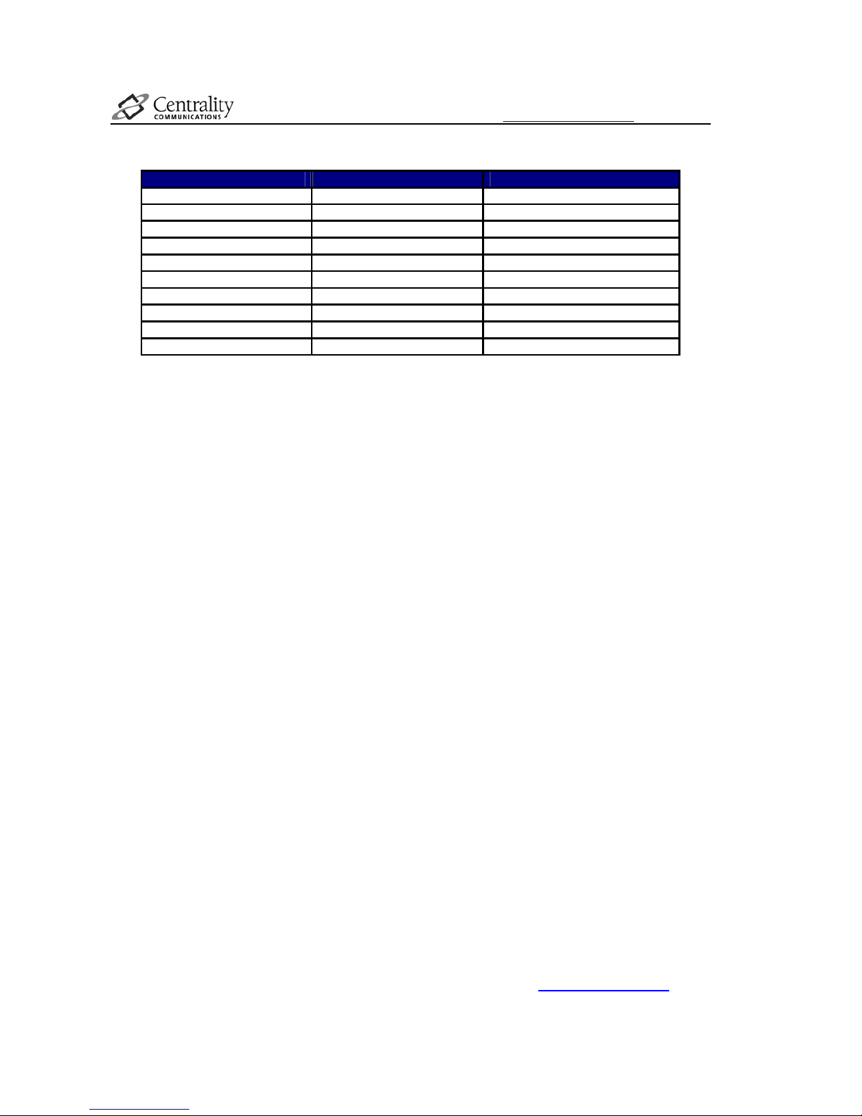
2.2 RISC Address Mapping
The ARM922T has a 32-bit address bus, which will be translated by the RISC interface into either an
access to cacheable data memory, non-cacheable data memory, or memory-mapped registers. Bits
<26:0> of the address are used as the physical address bus.
All address mapping registers must be inside the RISC interface. The RISC interface will be responsible
for all address decoding before it issues the command cycles to the system. The boot ROM should have
instructions about how to initialize these address-mapped registers. The programmer needs to provide
the system with the initialization routine.
• ROM & PCMCIA
The address mapping is defined starting from CPU reset vector (0x0000-0000). There is 512MB set
aside for ROM. However, not all of this space can be used. For security reasons, this memory must be
mirrored. Thus, the maximum size that can be set for the ROM cannot exceed 256MB. Also, because
the mirrored memory is laid out onto two sequential 256MB segments, accessing 0x0000-0000 and
0x1000-0000 directly will yield the same result.
The memory space from 512MB to 1GB is allocated to two PCMCIA sockets. Each socket takes 256MB
of memory.
• DSP Shared Memory & Extension Port
The Extension port takes 128MB space starting from 1GB address. And the DSP shared memory takes
another 128MB based on Extension port.
If the RISC reads from the reserved address space, a data abort operation will result. Writes to the
reserved address space have no effects.
• Internal Registers
Every peripheral device occupies 64K-byte space starting from 2GB to 3GB.
• System Memory
The system memory is between 3GB and 4GB. The actual memory size is also defined in the boot ROM
or by the memory auto-sizing program.
The following table shows the memory address mapping of Atlas™.
Page 14
**Preliminary and Confidential under NDA, DO NOT DISTRIBUTE
Atlas™ Programming Guide **Preliminary and Confidential under NDA, DO NOT DISTRIBUTE
- 13 -
Table 2. System Memory Mapping
Address Range Usage Resource Size
E800_0000~FFFF_FFFF
Reserved
384MB
E000_0000~E7FF_FFFF
Zero Bank
128MB
C000_0000~DFFF_FFFF
System Memory
512MB
8000_0000~BFFF_FFFF
Internal Registers
1GB
5000_0000~7FFF_FFFF
Reserved
768MB
4800_0000~4FFF_FFFF
DSP Shared Memory
128MB
4000_0000~47FF_FFFF
Extension Port
128MB
3000_0000~3FFF_FFFF
PCMCIA Socket 1
256MB
2000_0000~2FFF_FFFF
PCMCIA Socket 0
256MB
0000_0000~1FFF_FFFF
Flash/ROM
512MB
Page 15

**Preliminary and Confidential under NDA, DO NOT DISTRIBUTE
Atlas™ Programming Guide **Preliminary and Confidential under NDA, DO NOT DISTRIBUTE
- 14 -
2.3 Boot-up Control
There is a RISCINT_BOOT_UP register that can be used by software to record the boot-up status. If the
chip is boot-up from power on, then after boot-up software should set the COLD_BOOT bit in this
register. Otherwise, the software should set the WARM_BOOT bit.
Based on the value of this register, software can decide how to handle the following boot-up procedure.
When boot-up from NOR-Flash or ROM, the boot program needs to do re-direct the NOR-Flash/ROM
access to the shadowed SDRAM memory space somewhere between the boot-up. This is also done by
setting the COLD_BOOT bit. To make sure the setting taking effect as soon as possible, user can write
the FIFO_FLUSH bit in RISCINT_FIFO_FLUSH register right after set this Boot-up register.
RISCINT_BOOT_UP = 0x1;
RISCINT_FIFO_FLUSH = 0x3;
After the COLD_BOOT bit is set, all CPU access to address 0~0x0FFF_FFFF will be re-directed to the
system memory space (0xC000_0000~0xCFFF_FFFF). But the CPU can still access the NORFlash/ROM memory by issuing the address of it’s mirror image sitting on 0x1000_0000~0x1FFF_FFFF.
Due to the pipeline nature of the RISC core, after the Boot-up register been set, user CANNOT access
the ROM address space at once. It needs to insert at least one NOP between them.
Page 16

**Preliminary and Confidential under NDA, DO NOT DISTRIBUTE
Atlas™ Programming Guide **Preliminary and Confidential under NDA, DO NOT DISTRIBUTE
- 15 -
2.4 Wait State Control
Most peripherals in Atlas™ are in I/O clock domain (please refer to the section 6 “Clocks and Power
Manager”), while the RISC Subsystem is running at a higher system clock domain. So there is need for
inserting wait states when the RISC read those slow I/O devices.
Besides, due to the parastic capacitance in the silicon, the data read from a block that is far from the
CPU will have longer dealy. Sometimes the delay might be longer than one system clock cycle. In this
case, there is also need for inserting wait states.
There are totally 8 groups of wait state register bits (WS0~7); each is used to control the wait states of
one group of I/O devices. The allocation is as following:
• WS0 – RISC Interface, Interrupt Controller, OS Timer
• WS1 – DSP Interface, GPS Baseband, SDRAM Controller
• WS2 – LCD Controller, Reset Controller, Real-time Clock Controller
• WS3 – Power Manager, Resource Sharing Controller
• WS4 – Bus Arbiter, DMA Controller, Flash/ROM Controller, Camera Interface
• WS5 – USP0, USP1, USP2, USP3, Audio CODEC Interface
• WS6 – GPIO, Extension Port, SD/MMC Interface, Host Port, PCMCIA Interface
• WS7 – Bluetooth Baseband
Among those groups, WS0~WS3 are used to insert wait states for the blocks in system clock domain.
While WS4~6 are used to insert wait states of the blocks in I/O clock domain. WS7 is used for only
Bluetooth Baseband because it’s the only asynchronous device of the whole chip.
Because each group of wait state register bits are shared among several devices (except for WS7),
those devices will always have the same wait states setting. That is to say, if user want to increase wait
states for one block, then the other blocks in the same group will all have more wait states.
Page 17

**Preliminary and Confidential under NDA, DO NOT DISTRIBUTE
Atlas™ Programming Guide **Preliminary and Confidential under NDA, DO NOT DISTRIBUTE
- 16 -
2.5 Write Pulse Control
The wait states insertion can only solve the issues when RISC read slow devices. But if RISC is trying to
write the slow device, the write enable pulse has to be adjusted too. The write enable pulse width should
be exactly the same as the slow device’s clock period. Otherwise, the data might be written to the slow
device twice. This might be OK sometimes, but sometimes unkown result may occur.
The I/O clock domain can be programmed to run at ½ or ¼ of the clock frequency of the system (pleaser
refer to the section 6 “Clocks and Power Manager”). So there are two different configurations for the
write pulse width:
• When I/O clock is ½ of the system clock domain, the write enable pulse should be 2 system
clock cycles:
RISCINT_WIDTH = 0x10;
• When I/O clock is ¼ of the system clock domain, the write enable pulse should be 4 system
clock cycles:
RISCINT_WIDTH = 0x30;
Page 18

**Preliminary and Confidential under NDA, DO NOT DISTRIBUTE
Atlas™ Programming Guide **Preliminary and Confidential under NDA, DO NOT DISTRIBUTE
- 17 -
2.6 Timeout Control
When RISC accesses I/O device and the device has no response in a certain period, the RISC interface
will be timeout and generate an interrupt.
This certain period can be programmed by settting a 16-bit number in RISCINT_TIMEOUT register. By
default his register is not used at all. But if user like, he can easily enable the Timeout check by setting
the TIMEOUT_EN bit (bit<31> of RISCINT_TIMEOUT register).
When Timeout check is enabled and the device response is longer than the Timeout value, the RISC
interface will generate an interrupt to the CPU in RISCINT_TIMEOUT_INT register.
Page 19

**Preliminary and Confidential under NDA, DO NOT DISTRIBUTE
Atlas™ Programming Guide **Preliminary and Confidential under NDA, DO NOT DISTRIBUTE
- 18 -
3 DSP Subsystem
3.1 Operation Overview
The DSP used in Atlas™ processor acts as a acceleration computational parts for GPS, MP3, Image
processing etc. The DSP core is provided by Faraday Technology Corp. and is instruction compatible
with ADI’s ADSP2181 except for minor differences.
The DSP is an independent processor. It has it’s own program and data memory. The RISC core can
read/write data throught it’s IDMA port and can interrupt the DSP. The DSP can do data exchange
between it’s data or program memory and SDRAM by operating the DMA controller of DSP interface. It
can also control some of the peripherals such as DMA controller, serial port interface, interrupt controller,
GPIO and extension interface by accessing the peripherals’ registers.
Page 20
**Preliminary and Confidential under NDA, DO NOT DISTRIBUTE
Atlas™ Programming Guide **Preliminary and Confidential under NDA, DO NOT DISTRIBUTE
- 19 -
3.2 DSP Memory Address Mapping
The DSP core has three sets of buses to access three parts of memory named program memory, data
memory and program-data memory. For simplification, we call these three parts of memory PM, DMX
and DMY respectively. DMX is mapped to the DSP’s data memroy space, PM and DMY are mapped to
the DSP’s program memory space. Memory read/write instructions can only access DMY.
DMX and PM are further split to two parts, one part is accessed by DSP only (named DMX-in and PM-in
respectively), and another part can either be configured as accessed by DSP or accessed by DMA
controller (named DMX-swap and PM-swap respectively). This gives flexibility to change program or
move data when the DSP is running and is the compensation to small memory space. The DSP can
change memory settings by configure memory control registers and do DMA transfer by configure the
DMA control registers.
DMX-swap and PM-swap can be configured as single buffer or double buffer. When configured as
double buffer, the buffer is spitted into two parts: one part is accessed by the DSP and another part is
accessed by the DMA controller side. When configured as single buffer, the buffer is either accessed by
the DSP or accessed by the DMA controller.
NOTE: Though double buffer gives the flexibility of programming, it is hard to control it in
program because the DSP compiler does not support such features. And in most cases, it does
not significantly improve the performance. Use this feature with caution.
The total size of DMY is 4k WORD. 1k WORD is in DSP interface and can be accessed by the DSP or
the DMA controller, other 3k WORD is in GPS baseband module and can only be accessed by the DSP.
This 3k buffer can be used by DSP as normal data memory while GPS function is not activated. The
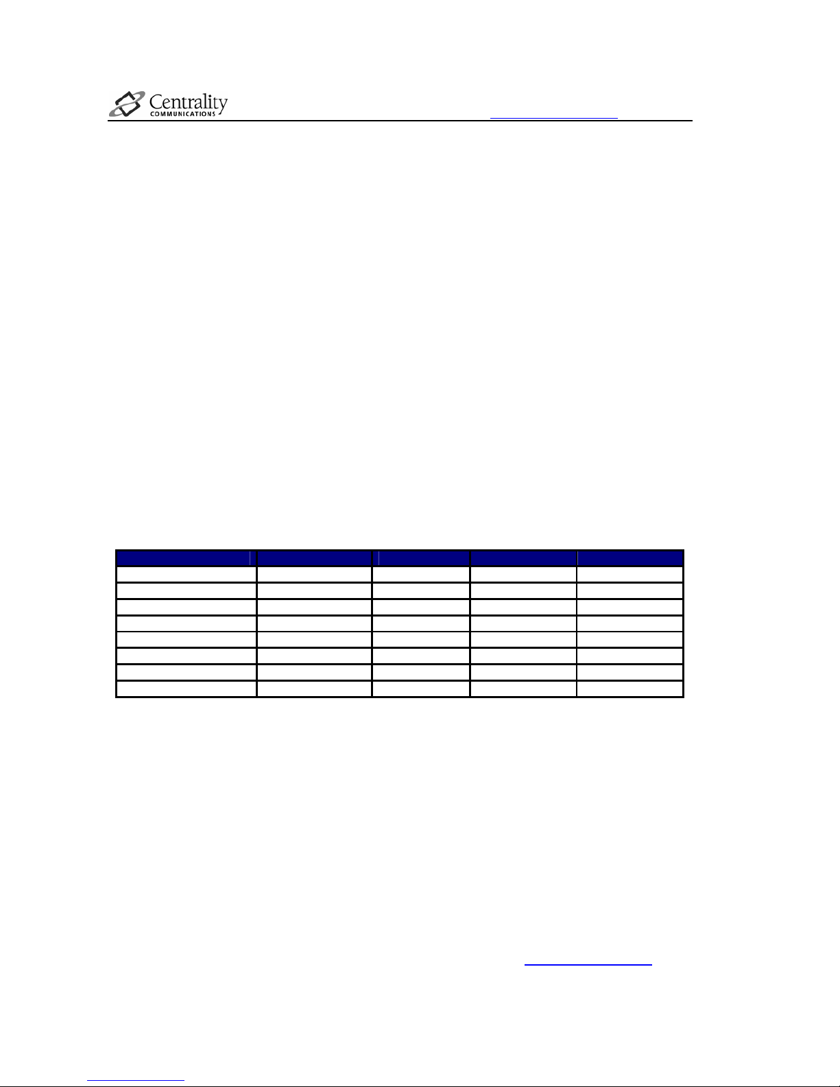
following table is the summary of the DSP memory spaces.
Table 3. DSP memory address mapping
Memory Starting Address Size(WORD) Word Length Accessed By
DMX-in 0x0000 (DM) 1024 16 DSP only
DMX-swap (single) 0x0400 (DM) 1024 16 DSP/SDRAM
DMX-swap (double) 0x0400 (DM) 512 16 DSP/SDRAM
DMY (DSP interface) 0x3c00 (PM) 1024 16 DSP/SDRAM
DMY (GPS baseband) 0x3000 (PM) 3072 16 DSP only
PM-in 0x0000 (PM) 1024 24 DSP only
PM-swap (single) 0x0400 (PM) 1024 24 DSP/SDRAM
PM-swap (double) 0x0400 (PM) 512 24 DSP/SDRAM
Page 21
**Preliminary and Confidential under NDA, DO NOT DISTRIBUTE
Atlas™ Programming Guide **Preliminary and Confidential under NDA, DO NOT DISTRIBUTE
- 20 -
3.3 DMA Operation
DMA of DSP interface can do data transfer between SDRAM and the DSP’s program or data memory.
The buffer DMX-swap, PM-swap and DMY all can be configured as accessed by DSP or accessed by
DMA controller. Because of the size limitation of the DSP’s memory, exchanging data between the
DSP’s memory and SDRAM gives the flexibality of accessing data and program with almost unlimited
size. The compiler of the DSP support overlay programming which means separate pages of program or
data memory overlay on the same address. By exchanging contents in DMX-swap and PM-swap, the
overlay feature can be used, because different data transfer from SDRAM to the DSP’s memory, it is
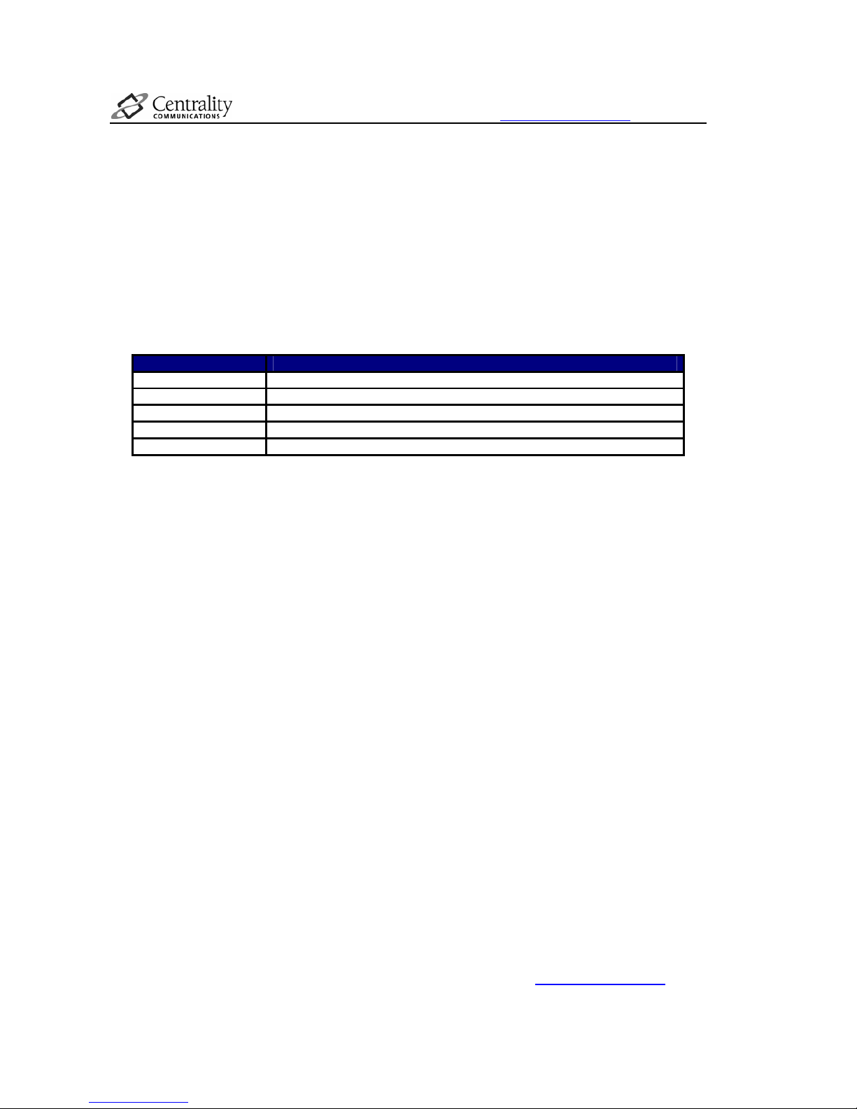
virtually to select different pages of memory. Generally, different memory of the DSP used by different
purpose as the following table shows:
Table 4. DSP memory usage guide
Memory Usage
DMX-in Global variables, constant arrays used by all pages of programs
DMX-swap Local variables, data need to be stored in SDRAM
DMY Global variables, constant arrays
PM-in Start up program, main routine, subroutines called frequently
PM-swap Other programs
3.3.1 Setting Memory Status
The DSP can set memory status by setting register DSP_MEM_MODE. To simplify programming, macro
can be used in DSP program to do memory status setting. The following is an example of macro that
setting DMA controller to access the DMX-swap buffer named sdram_dm:
{ let DMA controller access dm }
.macro sdram_dm;
ar = dm(DSP_MEM_MODE);
ar = setbit 3 of ar;
dm(DSP_MEM_MODE) = ar;
.endmacro;
Similar macros can be defined to set status of PM or DMY.
3.3.2 Starting DMA Transfer
The DSP starts DMA by writing DMA control registers including DSP_DMA_MODE and other DMA
parameter registers. Normally DMA parameters include physical address of SDRAM where DMA starts,
address offset of the DSP’s memory, x and y lengh of DMA. The DMA can be either one dimensional or
two dimensional. The latter one is mainly used on image processing. DSPDMA_PITCH_LO and
DSPDMA_PITCH_HI register should be set prior to starting two dimensional DMA transfer. When set y
length to 0, normal one dimensional DMA will occur. Set DMA parameters first and then set register
DSP_DMA_MODE to start a DMA.
NOTE1: At any time, there should be only one DMA running. Start another one after the previous
one completed.
NOTE2: For DMX-swap and DMY, the DSP memory address offset is in double WORD and is half
of the value addressed by DSP, for PM, address offset is the same seen by DSP. Address offset
is from the beginning of the buffer, so address offset 0 in DMX-swap means address 0x400,
address offset 1 means address 0x402 etc.
Page 22

**Preliminary and Confidential under NDA, DO NOT DISTRIBUTE
Atlas™ Programming Guide **Preliminary and Confidential under NDA, DO NOT DISTRIBUTE
- 21 -
NOTE3: X length is count of double word. But for PM, a 24bit WORD is treated as a 32bit double
word and valid data is in lower 24 bits.
A serial of macros can be defined to simplify programming. The following is an example to do DMA
between DMX-swap and SDRAM without waiting it completed.
{ do DMA transfer without waiting it complete}
{ syntax: transfer_dm_nowait(READ_DM/WRITE_DM, sdram_hi, sdram_lo, sram, xlen,
ylen); }
{ READ_DM is defined as 13 (2’b1101), WRITE_DM is defined as 5 (2’b0101) }
.macro transfer_dm_nowait(%0, %1, %2, %3, %4, %5);
i0 = DSPDMA_LENGTH_X;
dm(i0, m1) = %4; { xlength }
dm(i0, m1) = %5; { ylength }
dm(i0, m1) = %2; { SDRAM address low }
dm(i0, m1) = %1; { SDRAM address high }
ar = %3; { SRAM address }
dm(DMX_START_ADD) = ar;
ar = %0;
dm(DSPDMA_MODE) = ar; { do transfer }
.endmacro;
The following macro waits the DMA completed.
{ wait for transfer complete }
.macro wait_trans;
.local transfer_loop;
transfer_loop:
ar = dm(DSPDMA_MODE);
ar = tstbit 0 of ar; { completed? }
if ne jump transfer_loop;
.endmacro;
3.3.3 Endian Mode for DMA
Endian mode for DMA set the endian of DMA between SDRAM and DMX transfer. Default normal
endian mode is big endian and invert endian mode is little endian. Word format data read/write will use
little endian because the RISC uses the same endian mode. Byte format data read/write or bit stream
read/write will use big endian because it will concatenate MSB of next byte to the LSB of previous byte.
DMA between SDRAM and DMY transfer can only use little endian. The following is an example of
macro set to little endian.
{ set little endian mode }
.macro little_endian;
ar = dm(DSP_MEM_MODE);
ar = setbit 4 of ar;
dm(DSP_MEM_MODE) = ar;
.endmacro;
3.3.4 Byte Select Mode
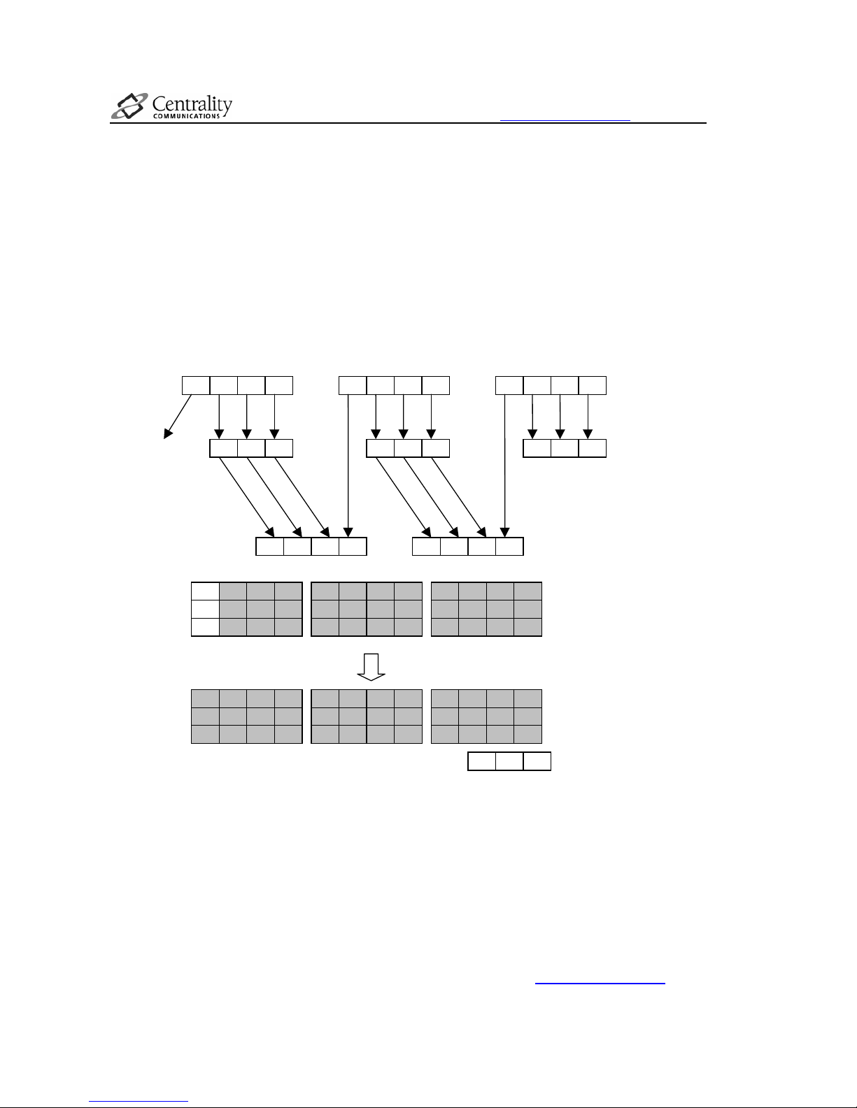
Writing data from SDRAM to DMX is on 32bit DWORD unit. In normal state, two lower bits of SDRAM
address will be ignored. It has a limitation that DSP has to load data from four-byte boundary. By set
BYTE_MODE bit to 1 in register DSP_BYTE_MODE, byte select mode is enabled. Byte select mode use
Page 23
**Preliminary and Confidential under NDA, DO NOT DISTRIBUTE
Atlas™ Programming Guide **Preliminary and Confidential under NDA, DO NOT DISTRIBUTE
- 22 -
the lowest 2 bit of SDRAM address as byte selection, load data from the selected byte address and read
four bytes each time. It will use the following method (assume lowest two bit of SDRAM address is 01):
First, four bytes aligned to DWORD boundary will be read in as A0 A1 A2 A3, A0 will be discarded and
last three bytes A1 A2 A3 will be put into storage registers S0 S1 S2. Then the second DWORD B0 B1
B2 B3 will be read in, B0 will concatenate to the storage registers to form a four-bytes DWORD and be
written into DMX-swap, last three bytes B1 B2 B3 will be put into storage registers. And this process
continuous with third read in DWORD appends C0 to B1 B2 B3 then store C1 C2 C3 etc. The total result
is x length multiply 4 numbers of bytes transfered to DMX from SDRAM at address which contains data
A1. If the lowest 2 bit of SDRAM is 10, data will transfer to DMX-swap from A2, if the lowest 2 bit of
SDRAM is 11, data will transfer to DMX-swap from A3. This method is useful while loading data from
unaligned address. When lowest two bit is 00, it will act as byte select not enabled, when lowest two bit
is not 00, x length should be increased by 1 to ensure actual number of DWORD written to DMX-swap is
x length.
Figure 2. DSP Byte Select Mode
The discard operation after the first read is optional. Normally, the first few bytes should be discarded.
But if the second DMA transfer need to concatenate data to the first DMA (for example, load data from a
circular buffer in SDRAM, the first transfer passes the end of buffer and the second transfer concatenate
the first one from the beginning of the buffer), the second DMA should not discard the first read in data
and data in storage registers.
A0 A1 A2 A3 B0 B1 B2 B3 C0 C1 C2 C3
Discarded
(Optional)
S0 S1 S2
A1 A2 A3 B0
S0 S1 S2 S0 S1 S2
B1 B2 B3 C0
…
Data In:
Data out:
A0 A1 A2 A3 B0 B1 B2 B3 C0 C1 C2 C3
…
D0 D1 D2 D3 E0 E1 E2 E3 F0 F1 F2 F3
…
G0 G1 G2 G3 H0 H1 H2 H3 I0 I1 I2 I3
…
…
A1 A2 A3 B0 B1 B2 B3 C0 C1 C2 C3
D1 D2 D3 E0 E1 E2 E3 F0 F1 F2 F3
G1 G2 G3 H0 H1 H2 H3 I0 I1 I2 I3
X0
Y0
Z0
…
Data In:
S0 S1 S2
= Storage registers
Page 24
**Preliminary and Confidential under NDA, DO NOT DISTRIBUTE
Atlas™ Programming Guide **Preliminary and Confidential under NDA, DO NOT DISTRIBUTE
- 23 -
3.4 Controlling Peripherals
The DSP can control the following peripherals
z GPS baseband
z Interrupt controller
z DMA controller
z GPIO
z Serial port
z Bluetooth interface
z Extension interface
The registers of GPS baseband and interrupt controller are mapped to the DSP’s data memory space,
registers of other peripherals are mapped to the DSP’s IO space. The following table is an overview of
address mapping:
Table 5. DSP peripheral registers address mapping
DSP Address Address space Device Mapped
0x0800~0x17FF DM GPS baseband
0x1800~0x19FF DM Interrupt controller
0x000~0x0FF IO DMA Controller
0x100~0x1FF IO General-purposed I/O
0x200~0x2FF IO Serial Port 0
0x300~0x3FF IO Serial Port 1
0x400~0x4FF IO Serial Port 2
0x500~0x5FF IO Serial Port 3
0x600~0x6FF IO Reserved
0x700~0x7FF IO Extension Interface
NOTE: The DMA controller refers to the system’s DMA controller. It is different from the DMA
controller of the DSP interface which only do DMA between SDRAM and the DSP’s memory.
Read or write these registers with normal data memory access instructions and IO instructions.
On default, peripherals are controlled by RISC. Each peripheral has it’s own control bit to determine
whether it is controlled by the RISC or controlled by the DSP. When one peripheral is controlled by the
RISC, the DSP can not access it’s registers.
Peripheral can interrupt the DSP, the interrupt are connected to the DSP’s IRQ2 input and can be set to
either level trigger or edge trigger.
For details of how to operate each peripheral, refer to the programming guide of corresponding
peripheral.
Page 25

**Preliminary and Confidential under NDA, DO NOT DISTRIBUTE
Atlas™ Programming Guide **Preliminary and Confidential under NDA, DO NOT DISTRIBUTE
- 24 -
3.5 DSP and RISC Cooperation
The DSP acts as an independent unit in the Atlas™ processor. It runs parallel with the RISC. Some
communication methods are available between the DSP and the RISC. The DSP and the RISC can
interrupt each other. The interrupt from the RISC are connected to the DSP’s IRQL1 input. The RISC
can access the DSP’s memory through it’s IDMA interface.
3.5.1 RISC Control DSP by Interrupt
The RISC should control DSP by following sequence:
1. Safely reset DSP and DSP interface and enable DSP memory output.
2. Write start up program and other program put in PM-in to DSP through IDMA interface.
3. Write data put in DMX-in to DSP through IDMA interface.
4. Other data and program will be loaded to DMX-swap, PM-swap and DMY should be in SDRAM.
5. Start DSP by write PM at address 0 through IDMA interface.
6. Interrupt the DSP with the subroutine entry address to let the DSP run it’s program.
7. Wait the interrupt signal sent by the DSP when it completed running it’s routine.
Following is example code of how to control the DSP
// Enable DSP interrupt
INT_RISC_MASK |= INT_MASK_DSP;
// reset DSP interface
RESET_SR |= RESET_SR_DIFACE_RST;
// enable DSP core and DSP interface clock
PWR_CLK_EN |= PWRCLK_DSP_EN;
// reset DSP
RESET_SR |= RESET_SR_DSP_RST;
// release DSP reset signal
RESET_SR &= ~RESET_SR_DSP_RST;
// release DSP interface reset signal
RESET_SR &= ~RESET_SR_DIFACE_RST;
// Allow Risc access DMA register
DSPREG_MODE = 1;
// Set UP SRAM OE
DSPDMA_MODE = 0x30000;
// Allow DSP access DMA register
DSPREG_MODE = 0;
for (i = 1; i < pm_in_size; i ++)
ProgramMemory[I] = pm_in_code[i];
WritePM(0, pm_in_code[0]);
DspInt = 0;
RISC_INT_DSP = (unsigned)routine_entry;
while(!DspInt);
The variable DspInt is a volatile variable, which should be set to no-zero in the RISC’s interrupt service
routine when receiving an interrupt from the DSP.
Page 26

**Preliminary and Confidential under NDA, DO NOT DISTRIBUTE
Atlas™ Programming Guide **Preliminary and Confidential under NDA, DO NOT DISTRIBUTE
- 25 -
On the DSP side, if nothing need to be done, DSP should be in IDLE mode to save power. Program
should accept interrupt from the RISC and run the routine code. After it finished the routine, send an
interrupt to RISC. The DSP should be programmed by the following sequence.
1. Enable interrupt of IRQ2, IRQL1 and other IRQ bits needed.
2. Enter the IDLE mode by executing idle instruction to wait an interrupt occur.
3. If the interrupt is from IRQL1 (eg. The RISC interrupts the DSP), jump to the subroutine with the
entry address given by the RISC.
4. After the subroutine completed, inform the RISC by sending an interrupt.
5. Go back to IDLE mode and wait for the next interrupt.
An example is given as following.
.module/ram/abs=0/seg = pm_in PM_IN_PROG;
.entry Subroutine;
StartDSP:
nop;
imask = 0x0300; /* #0000 0011 0000 0000 B; */
ena ints;
jump idle_loop;
irq2_srv:
jump irq2_int_srv;
nop; nop; nop;
irql1_srv:
ar = 1;
dm(GEN_REG2_L) = ar;
rti;
nop;
idle_loop:
icntl = 0x5; /* set irq2 edge */
idle;
ar = dm(GEN_REG2_L);
ar = pass ar;
if eq jump idle_loop;
i4 = dm(RISC_INT_DSP);
jump (i4);
return_addr:
ar = 0;
dm(DSP_INT_RISC) = ar;
jump idle_loop;
irq2_int_srv:
ena sec_reg;
ar = 0;
dm(GEN_REG2_L) = ar;
dis sec_reg;
rti;
Subroutine:
/* execute program */
/* when completed return by executing the following sentence */
jump return_addr;
Page 27

**Preliminary and Confidential under NDA, DO NOT DISTRIBUTE
Atlas™ Programming Guide **Preliminary and Confidential under NDA, DO NOT DISTRIBUTE
- 26 -
.endmod
NOTE: General purpose register GEN_REG2_L is used to differentiate interrupts from the RISC
and from the peripheral. If the interrupt is from peripheral, when go back from the interrupt
service routine, the DSP should directly go back to IDLE mode.
3.5.2 Data exchange between the RISC and the DSP
The RISC can directly access DSP’s memory through the DSP’s IDMA interface. The read or write
operation can be done parallel with the execution of the DSP. The DSP can not access it’s program
memory by instruction, so the only way to write to the PM-in buffer is through the IDMA interface.
IDMA interface is very convenient for the RISC to exchange data with the DSP, but it will take tens of
cycles to read or write a single WORD. So usually, the IDMA interface is used when the RISC initialize
the DSP and do a few WORDs of data exchange when the DSP is running. When large amount of data
need to be exchanged between the RISC and the DSP, use the DSP’s DMA function
Page 28

**Preliminary and Confidential under NDA, DO NOT DISTRIBUTE
Atlas™ Programming Guide **Preliminary and Confidential under NDA, DO NOT DISTRIBUTE
- 27 -
3.6 Differences between the DSP and ADI’s ADSP2181
Though the DSP is intruction compatible with the ADI’s ADSP2181, there are minor differences between
them. Programmer should take care of these differences when writing code.
3.6.1 Memory
As described above, the DSP’s internal memory are divided into three separate parts. Because
instructions accessing program memory are actually accessing the 16bit program-data memory, so there
is no PX register. Writing to PX register is a null operation, and reading from PX register always gets 16bit zero value.
3.6.2 Instructions
Some of the ADSP2181 instructions are not supported in the DSP. These instructions will be treated as
NOP. These non-supported instructions are listed in the following:
z Call or Jump on Flag In
z Modify Flag Out
z ENA INTS and DIS INTS
3.6.3 Biased-rounding mode
The biased rounding mode is also supported in Faraday’s DSP. Because bit 12 of memory mapped
register at address 0x3ff3 is used by other purpose, the rounding mode control bit is moved to bit 10 of
memory mapped register at address 0x3fff. When this bit is set to default value 0, unbiased rounding
mode is used, when this bit is set to 1, biased rounding mode is used.
3.6.4 Non-memory mapped registers
The definition of ICNTL is different from that of ADSP2181: the IRQ2 sensitivity is defined on bit 0 and
IRQ0 sensitivity is defined on bit 2.
The operation of counter CNTR (used for conditional jump/call that test CE instructions) is opposite to
that of ADSP2181. For instructions: IF NOT CE JUMP/CALL <addr>; If CE is true, CNTR will be
decremented by 1. If CE is not true then the top of count stack will be popped to CNTR.
The definition of PMOVLAY register is different from that of ADSP2181. Bit 7-4 of PMOVLAY register is
defines program-data memory overlay number and bit 3-0 defines program-code memory overlay
number. Writing 0xMN to PMOVLAY will set program-data memory overlay to M and program-code
memory overlay to N. If M or N is 0xF, the value will be unchanged. For PALM-II, there is no overlay
memory in program memory and PMOVLAY will always set to default value 0.
3.6.5 Memory mapped registers
The address and meaning of memory mapped registers are totally different from ADSP2181. The
description of those registers are listed in “F2016 16-bit DSP Microcomputer specification” and other
Atlas™ specified registers are listed in “Atlas™ Developer’s Manual”
3.6.6 Critical path limitation
There is critical path in the DSP on following instruction combination: I register read from data memory
followed by a data memory access using this I register. That is because data memory read will get
Page 29

**Preliminary and Confidential under NDA, DO NOT DISTRIBUTE
Atlas™ Programming Guide **Preliminary and Confidential under NDA, DO NOT DISTRIBUTE
- 28 -
effective data on data bus at the next cycle of read, while it should be put on the address bus at the
same cycle. The existing of critical path limites program with such instruction combination can not run
over 120MHz. Programmer should eleminate critical path instructions by inserting NOP or changing
instruction sequence.
Page 30

**Preliminary and Confidential under NDA, DO NOT DISTRIBUTE
Atlas™ Programming Guide **Preliminary and Confidential under NDA, DO NOT DISTRIBUTE
- 29 -
4 Dynamic Memory Interface
4.1 Operation Overview
Atlas™ supports the SDRAM interface at a maximum frequency of 100 MHz. The SDRAM Interface
supports up to four groups of SDRAMs. All the SDRAMs used should be of the same type, operate at
the same clock frequency and voltage. Each group can be placed in self-refresh mode independently.
The bit-width of the SDRAM can be either 16 or 32 bits wide. In 16-bit mode, two consecutive pieces of
data – each 16-bits wide - is fetched by the SDRAM interface and returned to system memory as a 32bit wide data. The memory mapping from SDRAM to internal system memory is done automatically
through hardware logic.
The Memory controller can be programmed into normal operation mode. It can also be put into sleep
mode by software or hardware.
Page 31

**Preliminary and Confidential under NDA, DO NOT DISTRIBUTE
Atlas™ Programming Guide **Preliminary and Confidential under NDA, DO NOT DISTRIBUTE
- 30 -
4.2 Pin Sharing
The MCS<3:2>, MCE<3:2> pins of SDRAM chip select 2,3 are shared with GPIO. If user needs SDRAM
chip select up to 3 or 4, user needs to program RSC block to enable the SDRAM controller’s control over
these pins.
The following sample code is used to enable the SDRAM controller’s control over these pins.
RSC_PIN_MUX |= 0x1e0; //use MCKE<2:3>,MCS_B<2:3> as SDRAM pins
PWR_PIN_RELEASE = 1; //release power manage pin holding
//Configure system clock;
…
//Configure SDRAM;
…
Page 32

**Preliminary and Confidential under NDA, DO NOT DISTRIBUTE
Atlas™ Programming Guide **Preliminary and Confidential under NDA, DO NOT DISTRIBUTE
- 31 -
4.3 Normal Operation
When booting from static memory interface or NAND flash, user need to program the Dynamic Memory
Interface for proper type of SDRAM used on the board.
Registers MEMC_SDTIM, MEMC_CFG, MEMC_SDCFG contain the timing information for the type of
SDRAM used on the board.
In the following example the MT48LC8M16A2-75 is used, the system & SDRAM interface is expected to
run at 96Mhz (T
SYS
=10.4ns). MT48LC8M16A2-75 is a 16bit width SDRAM. To form 2 group of 32-bit
SDRAM, 4 chips are needed.
For MEMC_SDTIM Register:
1) MEMC_SDTIM<3:0> defines Number of refresh cycles in initialization.
E.g. MT48LC8M16A2-75 requires 2 auto-refresh commands in initialization:
MEMC_SDTIM<3:0> = 2
2) MEMC_SDTIM <7:4> defines Number of NOP cycles after SDRAM Bank Active command.
E.g. For MT48LC8M16A2-75, t
RCD
= 20 ns. 2*T
SYS
= 20.8ns > t
RCD
:
MEMC_SDTIM<7:4> = 2
3) MEMC_SDTIM <11:8> defines Number of NOP cycles after SDRAM Precharge command.
E.g. For MT48LC8M16A2-75, t
RP
= 20 ns. 2*T
SYS
= 20.8ns > t
RP
:
MEMC_SDTIM<11:8> = 2
4) MEMC_SDTIM<15:12> defines Number of NOP cycles after SDRAM Refresh command.
E.g. For MT48LC8M16A2-75, t
RFC
= 66 ns. 7*T
SYS
= 72.8ns > t
RFC
:
MEMC_SDTIM<15:12> = 7
5) MEMC_SDTIM<26:16> defines Refresh Period, in number of 16*system memory clock (MCLK)
cycles.
E.g. MT48LC8M16A2-75 needs one auto-refresh every 15.625 us, 93*16*T
SYS
= 15.475us <
16.625 us
:
MEMC_SDTIM<26:16> = 93.
6) MEMC_SDTIM<28:27> defines CAS Latency.
E.g. To define CAS latency to be 3.
MEMC_SDTIM<28:27> = 3
7) MEMC_SDTIM<31:29> defines Memory Type.
E.g. MT48LC8M16A2-75 is a piece of 8M*16 SDRAM
MEMC_SDTIM<31:29> = 5
For MEMC_CONFIG Register:
1) MEMC_CONFIG<8> defines the SDRAM data bus width.
For example, 32-bit SDRAM data bus is used:
MEMC_CONFIG<8> = 1
2) MEMC_CONFIG<9> should be written as 1
3) All other register are for test purpose and should be written as 0
For MEMC_SDCFG Register:
Page 33

**Preliminary and Confidential under NDA, DO NOT DISTRIBUTE
Atlas™ Programming Guide **Preliminary and Confidential under NDA, DO NOT DISTRIBUTE
- 32 -
1) MEMC_SDCFG<3:0> defines the Number of chip select signals used.
For example, 2 group of SDRAM are used (2 chip select):
MEMC_SDCFG<3:0> = 0xC.
2) All other register are for test purpose and should be written as 0
If program is booting on static memory interface or NAND flash, the SDRAM can be configured as
following. The MEMC_POWER register needs to be programmed to initialize SDRAM.
//Configure System clock.
…
MEMC_SDTIM=0xB85D7222;
MEMC_CONFIG=0x200;
MEMC_SDCFG=0xc;
MEMC_POWER=0x4F;
Page 34

**Preliminary and Confidential under NDA, DO NOT DISTRIBUTE
Atlas™ Programming Guide **Preliminary and Confidential under NDA, DO NOT DISTRIBUTE
- 33 -
4.4 Wake-up Operation
After wake up from sleep, the SDRAM pins are hold by Resource Sharing Controller. User should
release the pin before initialize the SDRAM.
For the example used previously, the SDRAM should be initialized like following:
//Configure System clock.
…
MEMC_SDTIM=0xB85D7222;
MEMC_CONFIG=0x200;
MEMC_SDCFG=0xc;
PWR_SLEEP_STATUS = 0x8; // clear SDRAM_HOLD bit if wakeup from
sleep mode
MEMC_POWER=0x4F;
Page 35

**Preliminary and Confidential under NDA, DO NOT DISTRIBUTE
Atlas™ Programming Guide **Preliminary and Confidential under NDA, DO NOT DISTRIBUTE
- 34 -
4.5 Clock Switching Operation
User is able to switching system clock when the software is still running (Pleaser refer to the Chapter 6
“Clocks and Power Manager”). However when system clock is changed, the SDRAM interface timing
changed accordingly. User should change the timing register MEMC_SDTIM before clock switch actually
happen,
There are two types of clock switching:
1) Clock switch from PLL to 12MHz Oscillator
Before the switching actually happens, refresh period needs to be reconfigured; otherwise the refresh
period will be too big and does not meet the SDRAM requirement. When SDRAM refresh period is
changed to smaller value, user need to manually refresh SDRAM by reading one value from each
column in the SDRAM.
After the switching actually happens, user can change all other timing value for system performance.
However, if 12MHz is only a temporary setting (clock will be switched back to PLL soon), user does not
need to change those values.
2) Clock switch from 12MHz Oscillator to PLL
Before the switching actually happens, user needs to change the timing values except for refresh period
for correct SDRAM interface timing.
After the switching actually happens, user needs to change refresh period to an appropriate value to
make the system performance more effective.
The following sample codes detail the clocking switch from 96MHz to 12MHz, and then back to 96MHz:
volatile int TempReadValue;
int i;
…
MEMC_SDTIM= (MEMC_SDTIM & 0x7FF0000) | 0x 30000;
// read one data from each column for refresh purpose,
for(i=0;i<=0x2000000;i=i+512*4)
{
// SDRAM start address is mapped to 0xC0000000. This address
should be un-cacheable.
//the total SDRAM size is 0x2000000 in bye. Each column contains
512*4 byte.
TempReadValue = (volatile unsigned *) (0xC0000000 + i);
}
…
//Switch clock to 12MHz
…
//Change other timing value in MEMC_SDTIM for performance only.
…
//Change other timing value in MEMC_SDTIM to fit the new system clock.
…
//Switch clock to new system clock
…
Page 36

**Preliminary and Confidential under NDA, DO NOT DISTRIBUTE
Atlas™ Programming Guide **Preliminary and Confidential under NDA, DO NOT DISTRIBUTE
- 35 -
//Change refresh period in MEMC_SDTIM for performance only.
…
4.6 Self-refresh Mode
User can put SDRAM into self-refresh mode when needed.
However after SDRAM is put into self-refresh mode, if program fetches data from SDRAM again, the
SDRAM will be waked up automatically. So it is necessary to put the code on to CPU’s Instruction Cache
to make sure there is no SDRAM access after SDRAM is put into self-refresh mode.
The following codes will put SDRAM into self-refresh mode and should already be put on CACHE.
MEMC_POWER=0x7e;//make all chip select self refresh
…
MEMC_POWER=0x7f;//make all chip select out of self refresh
In the previous sample code there are 4 chip-select signals being used. But even if there are only 1, 2 or
3 chip-select signals being used, the code can still be used. The unused chip-select will not affect
anything if they are programmed to be GPIO.
Page 37

**Preliminary and Confidential under NDA, DO NOT DISTRIBUTE
Atlas™ Programming Guide **Preliminary and Confidential under NDA, DO NOT DISTRIBUTE
- 36 -
5 Static memory Interface
5.1 Operation Overview
The static memory interface has three functions:
• Boot-loader device during boot-up
• Storage device after boot-up.
• Extended interface for SRAM-like fixed latency I/O (FLIO) after boot-up.
When powered up, the central processor will boot up from the static memory interface. It will execute
boot code on the Flash or ROM. The boot code will read and copy the program from the Flash or ROM
into main system memory (SDRAM). In other words, in boot-up mode, the Flash/ROM will be shadowed
as part of system memory. However, after boot-up, the static memory interface can also be file related,
such as a storage device.
During boot-up, the static memory interface is mapped to the bottom of system address starting from
0x0000 0000. The code in the Flash or ROM should have an appropriate boot-loader at the base
address. The processor will execute the boot-loader first, during which it will configure the SDRAM and
initialize the hardware properly. The boot-load code will then copy the program code into system
memory. Two methods are available to execute this copy:
• The processor can read a chunk of 32-bit word from the static memory interface directly and
then it write the word to the system memory.
-- or --
• The processor can configure the static memory interface into DMA mode and wait until DMA
finishes.
After boot-up, the static memory interface can be considered a simple I/O device. It has a dedicated
DMA channel for data transfer to/from SDRAM. Most operations related to static memory will be act like
"file related" operations. For example, the system can save an image file into the Flash, just like it would
a regular storage device. Besides access through DMA, the processor may still be able to access the
static memory interface via memory mapped addresses. This comes in extremely useful since some FAT
related operations do not need to be done through DMA. In summary, the static memory interface will
have two operation modes after boot-up: memory mapped access ( direct access) and DMA. The static
memory interface register should be properly programmed for these different operational modes.
In DMA mode, the static memory interface uses DMA channel 4.
5.2 Instruction Access Mode
This is recommended for use only during boot-up.
The chip select 0 of Static Memory is set into Instruction Access Mode on reset. Other 3 chip select can
be configured into Instruction Access Mode by software. When RISC read data from address
0x1000_0000 to 0x1fff_ffff, the RISC Interface will redirect the read command to read data from Static
Memory Interface. The following table shows the mapping from different internal address to different chip
selects.
Table 6. Staitic Memory Chip Select Mapping
Chip select 0
0x1000_0000~ 0x13FF_FFFF
Chip select 1 0x1400_0000 ~ 0x17FF_FFFF
Page 38
**Preliminary and Confidential under NDA, DO NOT DISTRIBUTE
Atlas™ Programming Guide **Preliminary and Confidential under NDA, DO NOT DISTRIBUTE
- 37 -
Chip select 2
0x1800_0000 ~ 0x1bFF_FFFF
Chip select 3
0x1C00_0000 ~ 0x1FFF_FFFF
After reset, the address space from 0x0000_0000~0x0FFF_FFFF is shadowed with 0x1000_0000 ~
0x1FFF_FFFF. RISC will fetch the first instruction from address 0x0000_0000. When NAND_BOOT is
pulled-low, it is redirect to Static memory chip select 0.
In this mode, all the read are 32-bit wide. For different Static Memory Interface bit width, the 32-bit
DWORD is mapped as little endian, which is shown in the following figures:
Figure 3. Data Mapping in 8-bit External Data Bus
Figure 4. Data Mapping in 16-bit External Data Bus
In Instruction Access Mode any write command from RISC is ignored by the Static Memory Interface.
D<31:24> D<23:16> D<15:8>
D<7:0
>
Internal Data Bus (32-bit)
D<31:24>
D<23:16>
D<15:8>
D<7:0
>
External Data Bus (8-bit)
{A<23:2>, 2’b00}
{A<23:2>, 2’b11}
{A<23:2>, 2’b10}
{A<23:2>, 2’b01}
{A<23:2>, 2’b00}
D<31:24> D<23:16> D<15:8> D<7:0>
Internal Data Bus (32-bit)
D<31:16>
D<15:0>
External Data Bus (16-bit)
{A<23:2>, 2’b00}
{A<23:2>, 2’b10}
{A<23:2>, 2’b00}
Page 39

**Preliminary and Confidential under NDA, DO NOT DISTRIBUTE
Atlas™ Programming Guide **Preliminary and Confidential under NDA, DO NOT DISTRIBUTE
- 38 -
5.3 Direct Access Mode
In this mode, the Static Memory Interface will be considered as a simple IO device. It will respond to
RISC Access on address 0x1000_000 to 0x1FFF_FFFF. The address to chip select mapping is the
same as Instruction access mode. The different between this mode and Instruction Access Mode is as
following:
• Instruction Access Mode do now allow write, all write are treated as nop command.
• Direct Access Mode allow write to Static Memory.
• Instruction Access Mode’s access width is always 32-bit access.
• Direct Access Mode’s access width depends on the Static Memory Interface width set in the
ROM_CFG_CS register.
For 8bit width Static Memory Interface, user can only use 8-bit access in software, other access will
cause unknown operation on the Static Memory Interface. For 16bit width Static Memory Interface, user
can only use 16-bit access in software, other access will cause unknown operation on the Static Memory
Interface. The mapping from internal data access to static memory is the same in Instruction Access
mode.
Following sample code is used to access 8-bit width FLASH.
char FlashData;
int FlashAddress;
// Configure chip select 1 as direct access mode, 8 bit width
ROM_CFG_CS01= ROM_CFG_CS01 &0xFFFCFFFF;
FlashAddress=0x1;
// Direct read data from offset 0x01 in chip select 1
FlashData = (*((volatile unsigned char *)(0x14000000 + FlashAddress)));
// Perform a direct write to offset 0x01 in chip select 1
(*((volatile unsigned char *)(0x14000000+ FlashAddress))) = FlashData ;
Following sample code is used to access 16-bit width FLASH. In 16-bit access, the offset address should
be multiple of 2, because the address 0 is always zero in 16-bit width mode.
short FlashData;
int FlashAddress;
// Configure chip select 2 as direct access mode, 8 bit width
ROM_CFG_CS23 = (ROM_CFG_CS23 & 0xFFFFFFFC ) | 0x1 ;
// Direct read data from offset 0x02 in chip select 2
FlashAddress=0x2;
FlashData = (*((volatile unsigned short *)(0x18000000 + FlashAddress)));
// Perform a direct write to offset 0x01 in chip select 1
(*((volatile unsigned short *)(0x18000000 + FlashAddress)))= FlashData ;
Page 40
**Preliminary and Confidential under NDA, DO NOT DISTRIBUTE
Atlas™ Programming Guide **Preliminary and Confidential under NDA, DO NOT DISTRIBUTE
- 39 -
5.4 DMA Access Mode
In this mode, Static Memory Interface will perform bulk data read/write through internal FIFO, relieve the
burden of CPU to do every transaction.
The internal FIFO can talk with both RISC through read/write IO register and system memory through
DMA channel 4.
5.4.1 DMA read
User should properly configure ROM_CFG_CS01, ROM_CFG_CS23 for each chip select of Static
Memory Interface.
User should configure which chip select will be used in DMA, DMA will start from which address in the
chip select. This is done by configure ROM_START_ADDR Register.
SA<27:26> define which chip select to use in DMA as shown in the following table.
Table 7. Staitic Memory Chip Select Mapping
SA<27:26> 2’b00 2’b01 2’b10 2’b11
Chip select 0 Active in DMA
Chip select 1 Active in DMA
Chip select 2 Active in DMA
Chip select 3 Active in DMA
SA<25:0> decide the byte address from which to start DMA.
User should set the FIFO control register for proper direction, DMA length, refer to FIFO controller for
more information.
User should also configure DMA controller for proper direction, DMA length, System memory start
address. Refer to FIFO controller for more information.
Following sample code is for DMA Read.
#define DMA_MASK_BURST 0x08
#define DMA_MASK_WIDTH_0 0x00
#define DMA_MASK_TO_SDRAM 0x00
//configure dma and start dma,(the rom is not started yet, so no problem)
DMA_WIDTH0 = 0xfff;//using DMA_WIDTH0
DMA_CH4_XLEN = 32; //Transfer 32 DWORD
DMA_CH4_YLEN = 0x00;
DMA_CH4_CTRL = (DMA_MASK_BURST | DMA_MASK_WIDTH_0 | DMA_MASK_TO_SDRAM);
DMA_CH4_ADDR = (0x200000); //DMA start address in SDRAM
//configure Static Memory Interface
//reset fifo
ROM_FIFO_OP_REG=0x2;
ROM_FIFO_OP_REG=0x0;
ROM_INT_STATUS=0xfff;
//Static Memeory Interface register
Page 41

**Preliminary and Confidential under NDA, DO NOT DISTRIBUTE
Atlas™ Programming Guide **Preliminary and Confidential under NDA, DO NOT DISTRIBUTE
- 40 -
// Chip Select 1 use 16 bit data bus width
ROM_CFG_CS01= ROM_CFG_CS01 | 0x10000;
ROM_DMA_IO_LEN_REG = 32*2; //16 bit width , Transfer 32 DWORD
ROM_START_ADD = 0x2000000 ; //start from offset 0
ROM_DMA_IO_CTRL_REG=0x06;// DMA, FLUSH
// This is the FIFO_CTRL register setting for Static Memory Interface
ROM_FIFO_CTRL_REG=0xFC;
// set FIFO level check
ROM_FIFO_LEVEL_CHK_REG = ( ( 0xa << 20 ) | ( 0x8 << 10 ) | ( 0x4 ) );
//start read DMA
ROM_FIFO_OP_REG=0x01;
//wait for done status
while( (ROM_INT_STATUS&ROM_INT_MASK_DONE)==0 );
5.4.2 DMA write
User should properly configure ROM_CFG_CS01, ROM_CFG_CS23 for each chip select of Static
Memory Interface.
User should configure ROM_START_ADDR register. It is the same as DMA read.
User should set the FIFO control register for proper direction, DMA length, refer to FIFO controller for
more information.
User should also configure DMA controller for proper direction, DMA length, System memory start
address. Refer to FIFO controller for more information.
User should also configure ROM_WRITE_CTRL and ROM_WRITE_SEQ<2:0> registers for different
write mode.
5.4.2.1 Simple Write Mode
Static Memory Interface will perform one write operation for one data write.
User should program ROM_WRITE_CTRL with
• TWC= actual write cycle time;
• NWC= 1;
• ADINT=0;
• NSEQ=0;
The Interface timing diagram is should in the following figure.
Page 42
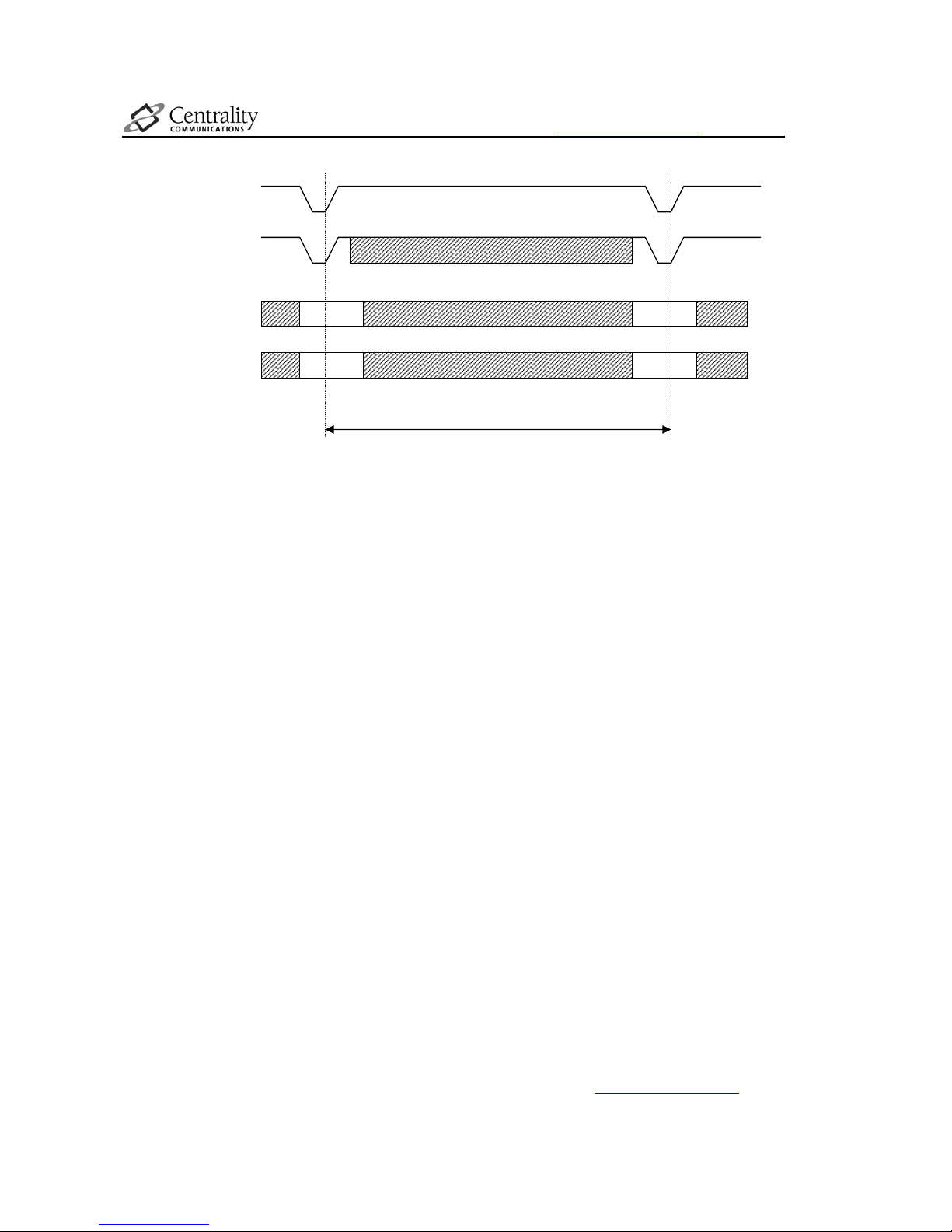
**Preliminary and Confidential under NDA, DO NOT DISTRIBUTE
Atlas™ Programming Guide **Preliminary and Confidential under NDA, DO NOT DISTRIBUTE
- 41 -
Figure 5. Static Memory Interface Simple WriteTiming
Notes: SA0, SA1 are address from ROM_START_ADDR. FD0, FD1 are data from FIFO. Depending
on Interface Width, one 32-bit data in FIFO will be splitted into 2 or 4 FD. The data in FIFO is
ordered as little endian.
Following sample code is for DMA Simple Write.
#define DMA_MASK_BURST 0x08
#define DMA_MASK_WIDTH_0 0x00
#define DMA_MASK_FROM_SDRAM 0x04
unsigned int twc;
DMA_WIDTH0 = 0xfff; //using DMA_WIDTH0 only
DMA_CH4_XLEN = 32;
DMA_CH4_YLEN = 0x00;
DMA_CH4_CTRL = (DMA_MASK_BURST | DMA_MASK_WIDTH_0 | DMA_MASK_FROM_SDRAM);
DMA_CH4_ADDR = 0x100000;//Start address of dat in SDRAM;
//configure Static Memory Interface
//reset fifo
ROM_FIFO_OP_REG=0x2;
ROM_FIFO_OP_REG=0x0;
ROM_INT_STATUS=0xfff;
//Static Memeory Interface register
// Chip Select 1 use 16-bit data bus width
ROM_CFG_CS01= ROM_CFG_CS01 | 0x10000;
ROM_DMA_IO_LEN_REG = 32*2; //16 bit width, Transfer 32 DWORD
ROM_START_ADD = = 0x2000000; //start from offset 0
ROM_DMA_IO_CTRL_REG=0x0;//dma, write to static memory , no flush
ROM_FIFO_CTRL_REG=0x00;
ROM_FIFO_LEVEL_CHK_REG=(0xb);//fifo level check
//twc is the actually write cycyle time, user needs to change the vaule to
//fit the actual system
twc=0xff;
FD0
T
twc
SA0
X_FCE_B
FWE_B
FA
FD
SA1
FD1
Page 43

**Preliminary and Confidential under NDA, DO NOT DISTRIBUTE
Atlas™ Programming Guide **Preliminary and Confidential under NDA, DO NOT DISTRIBUTE
- 42 -
ROM_WRITE_CTRL=
( ((0)&(0x3))<<12 | ((0)&(0x1))<<11 | ((1)&(0x7))<<8 | (twc)&(0xff) );
//start dma
ROM_FIFO_OP_REG=0x1;
//waiting for done status
while( (ROM_INT_STATUS&ROM_INT_MASK_DONE)==0 ) {
};
}
5.4.2.2 Fixed Sequence Write Mode
Static Memory Interface will perform several (max 4) write operation for one data write. The leading
several writes for one data write will be fixed data and address from registers ROM_WRITE_SEQ<2:0>.
User should program ROM_WRITE_CTRL with
• TWC= actual write cycle time;
• NWC= number of writes for one data write; (Max 4)
• ADINT=0;
• NSEQ=NWC-1; (Max 3 )
The Interface timing diagram is showed in the following figure. NWC is set to 3. There is totally 3 write
operation for one write cycle.
For the first data, there are 3 write operations. The First write operation write to the address stored in
ROM_WRITE_SEQ0 with data stored in ROM_WRITE_SEQ0. The second write operation write to the
address stored in ROM_WRITE_SEQ1 with data stored in ROM_WRITE_SEQ1. The last write operation
write to current address stored in ROM_START_ADDR with data from FIFO. The address in
ROM_START_ADD will increase automatically according to different Interface width.
For the second data, there are 3 write operations. The First write operation write to the address stored in
ROM_WRITE_SEQ0 with data stored in ROM_WRITE_SEQ0. The second write operation write to the
address stored in ROM_WRITE_SEQ1 with data stored in ROM_WRITE_SEQ1. The last write operation
write to current address stored in ROM_START_ADDR with data from FIFO. The address in
ROM_START_ADD will increase automatically according to different Interface width.
Page 44
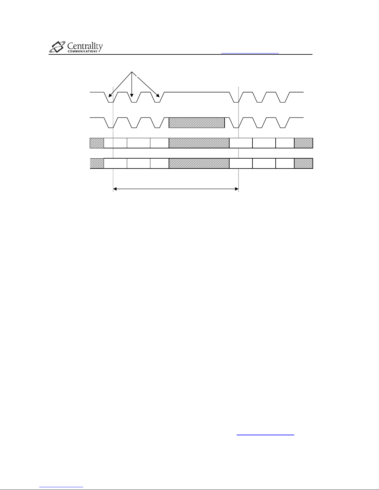
**Preliminary and Confidential under NDA, DO NOT DISTRIBUTE
Atlas™ Programming Guide **Preliminary and Confidential under NDA, DO NOT DISTRIBUTE
- 43 -
Figure 6. Static Memory Interface Fixed Sequence WriteTiming
Notes: SEQ0, SEQ1 are data and address from ROM_WRITE_SEQ0, ROM_WRITE_SEQ1
SA0, SA1 are address from ROM_START_ADDR. FD0, FD1 are data from FIFO. Depending on
Interface Width, one 32-bit data in FIFO will be splitted into 2 or 4 FD. The data in FIFO is ordered
as little endian.
User needs to change the configure of ROM_WRITE_CTRL In the previos sample code. And add the
configuration of registers ROM_WRITE_SEQ<1:0>.
#define DMA_MASK_BURST 0x08
#define DMA_MASK_WIDTH_0 0x00
#define DMA_MASK_FROM_SDRAM 0x04
unsigned int twc;
DMA_WIDTH0 = 0xfff; //using DMA_WIDTH0 only
DMA_CH4_XLEN = 32;
DMA_CH4_YLEN = 0x00;
DMA_CH4_CTRL = (DMA_MASK_BURST | DMA_MASK_WIDTH_0 | DMA_MASK_FROM_SDRAM);
DMA_CH4_ADDR = 0x100000;//Start address of dat in SDRAM;
//configure Static Memory Interface
//reset fifo
ROM_FIFO_OP_REG=0x2;
ROM_FIFO_OP_REG=0x0;
ROM_INT_STATUS=0xfff;
//Static Memeory Interface register
// Chip Select 1 use 16-bit data bus width
ROM_CFG_CS01= ROM_CFG_CS01 | 0x10000;
ROM_DMA_IO_LEN_REG = 32*2; //16 bit width, Transfer 32 DWORD
ROM_START_ADD = = 0x2000000; //start from offset 0
ROM_DMA_IO_CTRL_REG=0x0;//dma, write to static memory , no flush
T
twc
SEQ0
X_FCE_B
FWE_B
FA
FD
SEQ0
SEQ1
SEQ1
SA0
FD0
SEQ0
SEQ0
SEQ1
SEQ1
SA1
FD1
NWC=3
Page 45

**Preliminary and Confidential under NDA, DO NOT DISTRIBUTE
Atlas™ Programming Guide **Preliminary and Confidential under NDA, DO NOT DISTRIBUTE
- 44 -
ROM_FIFO_CTRL_REG=0x00;
ROM_FIFO_LEVEL_CHK_REG=(0xb);//fifo level check
//twc is the actually write cycyle time, user needs to change the vaule to
//fit the actual system
twc=0xff;
ROM_WRITE_CTRL=
(((2)&(0x3))<<12 | ((0)&(0x1))<<11 | ((3)&(0x7))<<8 | (twc)&(0xff));
ROM_WRITE_SEQ0 = sequence0;
ROM_WRITE_SEQ1 = sequence1;
//start dma
ROM_FIFO_OP_REG=0x1;
//waiting for done status
while( (ROM_INT_STATUS&ROM_INT_MASK_DONE)==0 );
5.4.2.3 Variable Sequence Write Mode
Static Memory Interface will perform several (max 4) write operation for one data write. Each write
operation’s address and data are got from FIFO.
User should program ROM_WRITE_CTRL with:
• TWC= actual write cycle time;
• NWC= number of writes for one data write; (Max 4)
• ADINT=1;
• NSEQ=0;
The Interface timing diagram is showed in the following figure. NWC is set to 3. There are totally 3 write
operations for one write cycle:
• The First write operation will read one 32-bit from FIFO, only LSB 28-bit are used as write
address. After that it will read another 32-bit from FIFO, only LSB 16/8-bit(depending on
interface width) are used as write data.
• The Second write operation will read one 32-bit from FIFO, only LSB 28-bit are used as write
address. After that it will read another 32-bit from FIFO, only LSB 16/8-bit(depending on
interface width) are used as write data.
• The Third write operation will read one 32-bit from FIFO, only LSB 28-bit are used as write
address. After that it will read another 32-bit from FIFO, only LSB 16/8-bit(depending on
interface width) are used as write data.
Page 46
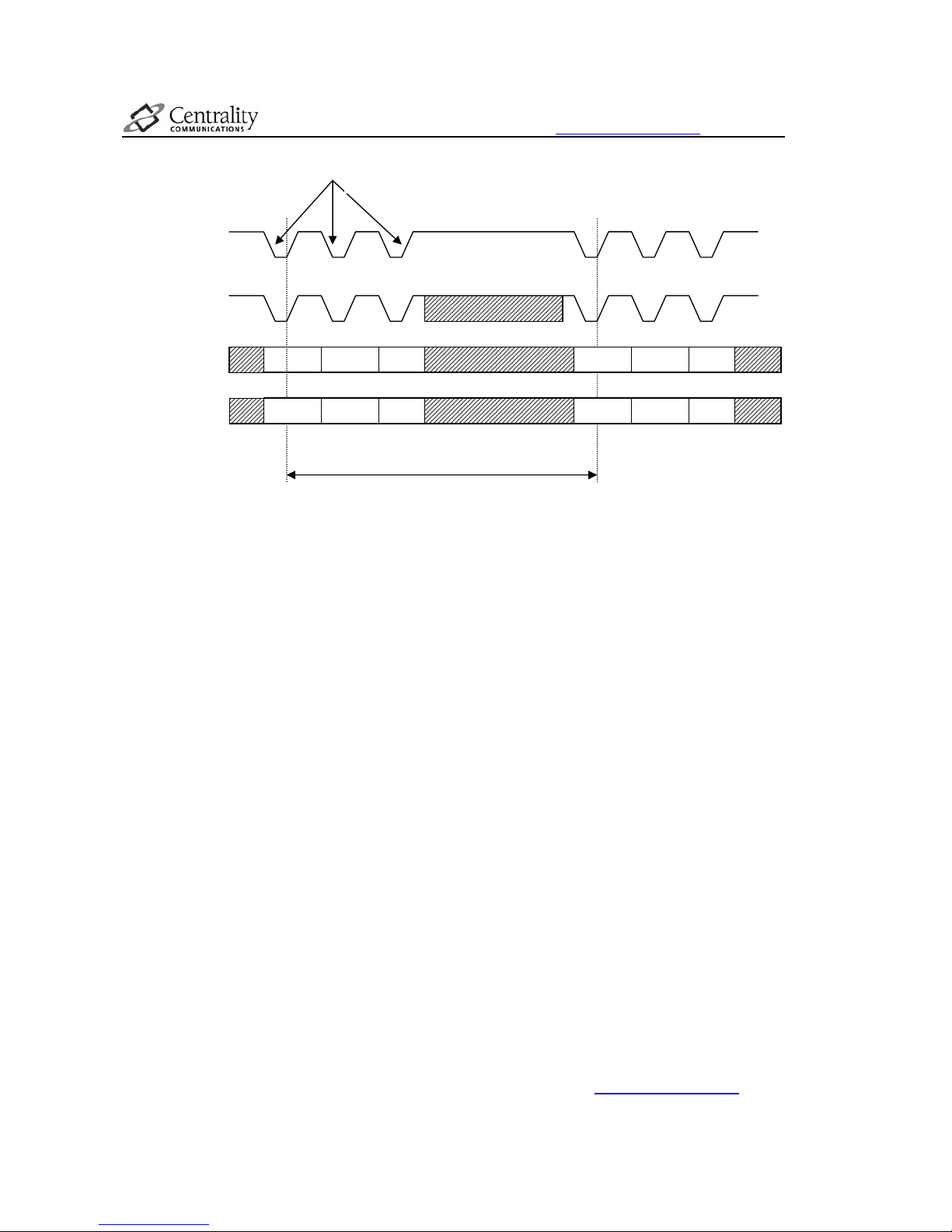
**Preliminary and Confidential under NDA, DO NOT DISTRIBUTE
Atlas™ Programming Guide **Preliminary and Confidential under NDA, DO NOT DISTRIBUTE
- 45 -
Figure 7. Static Memory Interface Fixed Sequence WriteTiming
Notes: FA0 … FA6, FD0 .. FD6 are data from FIFO. Each 32-bit data in FIFO only contain only FA
or on FD. ROM_START_ADDR, ROM_WRITE_SEQ<2:0> registers will not be used in this mode.
Their value will be unknown.
Following code is the sample for DMA variable sequence write.
#define DMA_MASK_BURST 0x08
#define DMA_MASK_WIDTH_0 0x00
#define DMA_MASK_FROM_SDRAM 0x04
unsigned int twc;
DMA_WIDTH0 = 0xfff; //using DMA_WIDTH0 only
DMA_CH4_XLEN = 32;
DMA_CH4_YLEN = 0x00;
DMA_CH4_CTRL = (DMA_MASK_BURST | DMA_MASK_WIDTH_0 | DMA_MASK_FROM_SDRAM);
DMA_CH4_ADDR = 0x100000;//Start address of dat in SDRAM;
//configure Static Memory Interface
//reset fifo
ROM_FIFO_OP_REG=0x2;
ROM_FIFO_OP_REG=0x0;
ROM_INT_STATUS=0xfff;
//Static Memeory Interface register
// Chip Select 1 use 16-bit data bus width
ROM_CFG_CS01= ROM_CFG_CS01 | 0x10000;
//16 bit width, Transfer 32 DWORD, both data and address are get from FIFO
ROM_DMA_IO_LEN_REG = 32*2*2;
ROM_START_ADD = = 0x2000000; //start from offset 0
ROM_DMA_IO_CTRL_REG=0x0;//dma, write to static memory, no flush
ROM_FIFO_CTRL_REG=0x00;
T
twc
FA0
X_FCE_B
FWE_B
FA
FD
FD0
FA1
FD1
FA3
FD3
FA4
FD4
FA5
FD5
FA6
FD6
NWC=3
Page 47

**Preliminary and Confidential under NDA, DO NOT DISTRIBUTE
Atlas™ Programming Guide **Preliminary and Confidential under NDA, DO NOT DISTRIBUTE
- 46 -
ROM_FIFO_LEVEL_CHK_REG=(0xb);//fifo level check
//twc is the actually write cycyle time, user needs to change the vaule to
//fit the actual system
twc=0xff;
ROM_WRITE_CTRL=
(((0)&(0x3))<<12 | ((1)&(0x1))<<11 | ((3)&(0x7))<<8 | (twc)&(0xff));
//start dma
ROM_FIFO_OP_REG=0x1;
//waiting for done status
while( (ROM_INT_STATUS&ROM_INT_MASK_DONE)==0 );
Page 48

**Preliminary and Confidential under NDA, DO NOT DISTRIBUTE
Atlas™ Programming Guide **Preliminary and Confidential under NDA, DO NOT DISTRIBUTE
- 47 -
6 Clocks and Power Manager
6.1 Operation Overview
There are totally 4 clock sources in Atlas™: 32.768 KHz Oscillator, 12 MHz Oscillator, and two
programmable PLL’s. And there are 7 clock domains:
• System Clock Domain (including DSP, Memory Controller, LCD Controller, System Arbiter, and
other system control modules)
• CPU Clock Domain (including the ARM922T RISC core)
• I/O Clock Domain (including the I/O Bridge, DMA Controller, and all the peripheral modules)
• External Memory Clock Domain (only for external SDRAM chips)
• USB Clock Domain (only for USB device core)
• Bluetooth Clock Domain (only for Bluetooth baseband core)
• External Clock Domain (only for External Clock Output)
Except for the Bluetooth Clock Domain (which is clocked by external Bluetooth RF module), each clock
domain can be programmed to select one of these 4 clock sources. Besides of that, some clock domains
can be configured to different clock ratios.
NOTE: CPU is actually involved with two clock domains: CPU Clock Domain and System Clock
Domain. The reason is that the CPU has two clock inputs: one for core clock and the other for
bus clock. The bus clock is always the same as Atlas™ system clock (i.e. in System Clock
Domain); the core clock is in CPU Clock Domain.
User can change the PLL output frequency from 12MHz up to 240MHz by programming the PLL
Configuration Registers (PWR_PLL1_CONFIG & PWR_PLL2_CONFIG).
To save the power consumption, most blocks’ clock can be disabled independently by software. And for
even lower power consumption, the Atlas™ can be forced into the sleep mode.
NOTE: When SDRAM is used as system memory, user needs to be careful when changing the
system clock rate. In some cases, the SDRAM refresh rate needs to change accordingly. Please
refer the section 4.4 “Clock Swithcing Operation” for more details.
Page 49

**Preliminary and Confidential under NDA, DO NOT DISTRIBUTE
Atlas™ Programming Guide **Preliminary and Confidential under NDA, DO NOT DISTRIBUTE
- 48 -
6.2 Change Clock Source
The Atlas™ system can be programmed to use either PLL1 or PLL2 as the clock source. In addition, it
can also select the oscillator (12MHZ or 32.768KHz) outputs as the clock source. The switching of the
clocks can take place in real-time while Atlas™ is running. If the 32.768KHz oscillator output is
selected, the whole system will run at the same 32.768KHz frequency. Otherwise, different parts of the
system can be switched to different clock sources independently:
• The system clocks (including the CPU bus clock, the DSP clock, the GPS clock, the LCD clock,
etc.), external memory clock, and internal I/O clocks can only be switched to different clock
sources at the same time.
• The CPU clock, USB clock, and the External clock outputs can be switched to different clock
sources separately.
During the Atlas™ boot-up, the following clock switching steps need to be followed:
• After reset, both PLL1 and PLL2 are in power-down mode, and will be bypassed by the system
clock. The clock will use the 12MHz oscillator by default.
• The boot-up program will set up the clock configuration registers (PWR_PLL1_CONFIG) and
turn on the PLL.
• After the PLL is stable, the boot-up program will switch the clock from the 12MHz oscillator to the
PLL.
NOTE: Before switch the clock source to PLL, make sure the PLL has already powered up and
stable.
Here is an example to switch the clock source to PLL1:
//All clocks switch to pll1
PWR_CLK_SWITCH = 0x55;
for (i=1;i<=10;i++);
NOTE: It’s suggested to delay for several cycles for the operations for waiting the clock switch
finishes.
In some cases, the whole system can run from a single clock source and the other unused PLL(s) can
be powered down to save power.
Page 50

**Preliminary and Confidential under NDA, DO NOT DISTRIBUTE
Atlas™ Programming Guide **Preliminary and Confidential under NDA, DO NOT DISTRIBUTE
- 49 -
6.3 Change Clock Ratio
Although the system clocks, external memory clock, and internal I/O clocks are using the same clock
source, they can be programmed to different clock ratios by configuring the clock ratio register:
• System clocks can be programmed to be either 1/1 or ½ of the clock source
• External memory clock can also be programmed to be 1/1 or ½ of the System clocks
• Internal I/O clocks can be programmed to be ½ or ¼ of the System clocks
6.3.1 Change the System and I/O Clock Ratio
Here is an example to change the system clock to be ½ of the clock source, and the I/O clock to be ¼ of
the clock source.
//system clock ratio = 1:2, I/O clock ratio = 1:4
PWR_CLK_RATIO = 0x3;
for (i=1;i<=10;i++);
NOTE: It’s suggested to delay for several cycles for the operations for waiting the clock ratio
change finishes.
In the above example, if the clock source is 100 MHz, then the system clock will be 50 MHz and the I/O
clock will be 25 MHz. The capability of changing system clock ratio provides a way to achieve better
performance/power ratio. For example, for those applications needs intensive CPU power but less data
input/output, user can configure the system clock to be half of the CPU clock. Besides, the capability of
changing I/O clock ratio can better fit applications requirements of the I/O clock speed.
One thing needs to be noted is: when user configure the system clock ratio to be 1:2, then it means the
CPU may not be in Fast Bus mode
1
anymore. User can still configure the CPU to be in Fast Bus mode in
this case, but then the CPU core clock will be the same as the bus clock (system clock), i.e. ½ of the
clock source. Or, user can configure the CPU to be in Synchronous or Asynchronous mode, i.e. CPU
core clock is twice of the CPU bus clock. This is called Turbo mode and more details can be found in the
section 6.5.2.
Besides, when the I/O clock ratio is changed, the RISCINT_WIDTH register needs to be changed
accordingly.
// When I/O clock ratio is 1:2
RISCINT_WIDTH = 0x10;
// When I/O clock ratio is 1:4
RISCINT_WIDTH = 0x30;
6.3.2 Change the External Memory Clock Ratio
The following example shows the changing of external memory clock ratio:
//memory clock ratio 1:2
MEMC_CFG = 0x300;
for (i=1;i<=10;i++);
1
ARM922T has three different clocking modes: Fast Bus mode, Synchronous mode, and Asynchronous mode. Please refer to the
ARM922T datasheet for more details.
Page 51

**Preliminary and Confidential under NDA, DO NOT DISTRIBUTE
Atlas™ Programming Guide **Preliminary and Confidential under NDA, DO NOT DISTRIBUTE
- 50 -
The capability of changing the clock ratio provides a further tunning of performance/power ratio. For
example, for those applications do not need high memory bandwidth but has intensive DSP calculations,
then we can configure the memory clock to be half of the system clock.
NOTE: To change the external memory clock ratio must be done when program is running either
on Flash/ROM or in Instruction Cache. Otherwise, unexpected result may happen.
Page 52

**Preliminary and Confidential under NDA, DO NOT DISTRIBUTE
Atlas™ Programming Guide **Preliminary and Confidential under NDA, DO NOT DISTRIBUTE
- 51 -
6.4 Change PLL Frequency
To change the PLL frequency, user needs to program the PLL configuration registers
(PWR_PLL1_CONFIG & PWR_PLL2_CONFIG). And it’s suggested to following the steps as:
1. Switch the clock source to other PLL or oscillators (if the current PLL is in use)
2. Stop the current PLL
3. Re-configure the current PLL
4. Start the current PLL
5. Wait for PLL stable
6. Switch the clock source back to the current PLL
Here is a basic example showing the above programming steps:
// Switch the clock source to PLL2
PWR_CLK_SWITCH=0xAA;
for(i=1;i<=10;i++);
// Stop PLL1
PWR_CLK_CTRL = 0x2;
// Configure PLL1
PWR_PLL1_CONFIG = 0x3099; //150Mhz
// Start PLL1
PWR_CLK_CTRL = 0x03;
for(i=1;i<=40;i++); // wait for PLL stable
// Switch back to PLL1
PWR_CLK_SWITCH=0x55;
for(i=1;i<=10;i++);
NOTE: Due to the PLL limitation, the output frequency has to be the multiple of 6 MHz (half of the
12 MHz Crystal input). Or, in another words, the pre-divider (MS<5:0>) has to be set to 1 or 2.
Page 53

**Preliminary and Confidential under NDA, DO NOT DISTRIBUTE
Atlas™ Programming Guide **Preliminary and Confidential under NDA, DO NOT DISTRIBUTE
- 52 -
6.5 Power Mode
The Atlas™ can operate at different operation modes:
• Turbo mode: the CPU runs at its peak frequency (higher than System clocks)
• Normal mode: the CPU runs at its normal frequency (equal to the System clocks)
• Idle mode: the CPU enters IDLE mode and each of the other blocks in system can be disabled
separately too
• Standby mode: the whole system runs at the 32.768KHz
• Sleep mode: the most of the system stops clocking except the RTC and Power Manager
The Atlas™ contains power management logic that controls the transition between all these different
modes of operations. This part of logic can only be controlled by the RISC but not DSP Core.
6.5.1 Normal Mode
Normal mode is the normal operating mode of the Atlas™: all power supplies are enabled, all clocks are
running, and every on-chip resource is functional. And the CPU runs at the same clock rate as the other
part of the system (except for the I/O peripherals). Under usual conditions, the chip enters normal mode
after successful power-up and reset of the part.
6.5.2 Turbo Mode
In Turbo Mode, the CPU clock runs at a higher clock rate (than System clocks) that is either
asynchronous to or double of the System clocks. For example, the system clock runs at 100MHz, while
the CPU runs at 200MHz or even 240MHz.
To configure the Atlas™ into Turbo mode, there are two things need to be done:
1. Configure the CPU into Synchronous or Asynchronou mode
2. Configure the CPU core clock (CPU Clock Domain) and bus clock (System Clock Domain)
Here is an example to configure the CPU in Synchronous or Asynchronous clock modes:
LDR r0, =0x0
IF :DEF:ARMCPU_ASYNC_MODE
IF ARMCPU_ASYNC_MODE = "ON"
INFO 0, "Using ARM922 Asynchronous Mode"
LDR r0, =0xc0000000
ENDIF
ENDIF
IF :DEF:ARMCPU_SYNC_MODE
IF ARMCPU_SYNC_MODE = "ON"
INFO 0, "Using ARM922 Synchronous Mode"
LDR r0, =0x40000000
ENDIF
ENDIF
As for how to configure the CPU core clock and bus clock, please refer to the previous sections.
6.5.3 Idle Mode
Page 54

**Preliminary and Confidential under NDA, DO NOT DISTRIBUTE
Atlas™ Programming Guide **Preliminary and Confidential under NDA, DO NOT DISTRIBUTE
- 53 -
Idle mode allows software to put each block into idle, even the RISC itself.
When RISC is in idle, it continues to monitor interrupt service requests on or off-chip. When an interrupt
occurs, the RISC is reactivated. The RISC enters the idle mode by executing a three-instruction
sequence consisting of the CP15 instruction ‘disable clock switching’, a load from non-cacheable
memory location (C=B=0), and the CP15 instruction ‘wait for interrupt’. Following are the code example
of force RISC into idle mode:
ldr r1, =0xA8000000 ; just an arbitrary uncachable location
mcr p15, 0, r0, c15, c2, 2 ; disable clock switching
ldr r0, [r1]
mcr p15, 0, r0, c15, c8, 2 ; go idle
nop
nop
mcr p15, 0, r0, c15, c1, 2 ; (re)enable clock switching
The RISC can also put other blocks into idle, including the DSP Core
1
, by programming a corresponding
register bit in PWR_CLK_EN to disable or enable the clock of that block. Here is an example:
// enable all block's clock
PWR_CLK_EN = 0x1FFFF;
6.5.4 Standby Mode
In Standby Mode, the whole system runs at the clock rate the same as the RTC (32.768KHz). This is
useful when sometimes the system is doing a non-urgent job but need to stay alive for a long time.
To enter the Standby mode, user just needs to write:
// Switch all clocks to 32KHz
PWR_CLK_SWITCH = 0x03;
for(i=1;i<=10;i++);
But when system is using SDRAM as the external system memory, it’s impossible to use the clock as
low as 32.768 KHz. It’s too slow for the SDRAM refresh. In this case, user might want to use a higher
frequency crystal or oscillator (e.g. 1MHz) to replace the 32.768 KHz crystal.
6.5.5 Sleep Mode
Sleep mode offers the greatest power savings to the user and consequently the lowest level of available
functionality. In the transition from run or idle to sleep mode, the Atlas™ performs an orderly shutdown of
on-chip activity, applies an internal reset to the processor, and then negates the PWR_EN pin indicating
to the external system that the Atlas™ is in sleep mode. Running off the 32.768 kHz Oscillator, the sleep
state machine watches for a preprogrammed wake-up event to occur, after which it asserts PWR_EN pin,
and steps through an orderly wake-up sequence. When the power supply and clocks are stable, the
power manager brings the Atlas™ out of reset.
There are two methods to enter the sleep mode: by software or by hardware. The usage of software
sleep is: when power down button is pressed, the software will stops all the current jobs being running;
and then configure the Atlas™ to sleep mode in the following sequence:
• Enable 12MHz Oscillator power down in sleep mode (PWR_CONFIG) – only when if needed
1
The DSP Core has its own 'idle' mode too. By issuing IDLE instruction, the DSP Core will wait indefinitely in a low power state
until an interrupt to DSP occurs. That 'idle' is in different level with this idle mode. Please refer to the DSP section for more details.
Page 55

**Preliminary and Confidential under NDA, DO NOT DISTRIBUTE
Atlas™ Programming Guide **Preliminary and Confidential under NDA, DO NOT DISTRIBUTE
- 54 -
• Set wakeup event (PWR_WAKEUP_EN)
o It can be waked up by GPIO, or,
o It can be waked up by Real-time Clock Alarm
• Set wakeup wait time for power ramp and Oscillator stable (PWR_WAIT_TIME)
• Set force sleep bit (PWR_CTRL)
Here is an example of the software sleep:
#define RTC_DIVISION 1000
#define ALARM_VALUE 1000
#define WAIT_OOK_TIME 0xff
#define WAIT_OPU_TIME 0xff
// Enable 12MHz crystal power down in sleep mode
PWR_CONFIG=0x01;
// Set real-time clock division
RTC_DIV = RTC_DIVISION;
RTC_COUNTER = 0x0;
// Set Alarm value
RTC_ALARM = ALARM_VALUE; // alarm value
// Set wakeup event
PWR_WAKEUP_EN = 0x80000000; // wakeup by alarm
PWR_WAIT_TIME = (WAIT_OOK_TIME | (WAIT_OPU_TIME << 16));
// Enter sleep mode
PWR_CTRL=0x01;
While the hardware sleep is for another usage: when the system battery or power source is fail to
provide enough current to Atlas™, the Atlas™ will go to sleep mode automatically to save the power
consumption. This is done by the BATT_FAULT or VDD_FAULT pin. The power-down sequence is
almost the same as the software sleep, except user does not need to set the force sleep bit in
PWR_CTRL register.
When Atlas™ is waked up from the sleep mode, user can read the PWR_SLEEP_STATUS register to
find out if it’s a wakeup from software sleep or hardware sleep.
Page 56

**Preliminary and Confidential under NDA, DO NOT DISTRIBUTE
Atlas™ Programming Guide **Preliminary and Confidential under NDA, DO NOT DISTRIBUTE
- 55 -
7 GPIO
7.1 Operation Overview
The Generous Purpose Input Output (GPIO) logic of the Atlas™ processor controls 28 pins through the
use of 16 registers which control the pin direction (input or output) pin function, pin state (outputs only),
pin level detection (inputs only).
Some of the GPIOs can be used to bring the Atlas™ processor out of Sleep mode.
In all the following configurations, PWR_PIN_RELEASE must be set to 1 so that Resource Sharing
Controller does not control GPIO pins anymore.
Page 57

**Preliminary and Confidential under NDA, DO NOT DISTRIBUTE
Atlas™ Programming Guide **Preliminary and Confidential under NDA, DO NOT DISTRIBUTE
- 56 -
7.2 Configure GPIO Pin Sharing
• GPIO<24:27> are shared with memory interface pin MCKE<2:3>, MCS_B<2:3>.
RSC_PIN_MUX &= 0xfffffe1f; //use MCKE<2:3>, MCS_B<2:3> as GPIO<24:27>
PWR_PIN_RELEASE = 1; //release power manage pin holding
• GPIO<23:21> are shared with USP0 port.
RSC_PIN_MUX &= 0xfffeffff; //use SCLK0, TFS0, RFS0 as GPIO<21:23>
PWR_PIN_RELEASE = 1; //release power manage pin holding
• GPIO<20:16> are shared with the JTAG interface.
• GPIO<20:16> are used as JTAG pin when JTAG mode is selected on reset (TEST_MODE<1:0>
=2’b10 on reset). Otherwise those pins are used as GPIO pins.
• GPIO<15:8> are shared with the LCD Controller.
RSC_PIN_MUX &= 0xfffffffe; //use LDD<8:15> as GPIO<8:15>
PWR_PIN_RELEASE = 1; //release power manage pin holding
Page 58

**Preliminary and Confidential under NDA, DO NOT DISTRIBUTE
Atlas™ Programming Guide **Preliminary and Confidential under NDA, DO NOT DISTRIBUTE
- 57 -
7.3 Configure GPIO as Input
The following codes configure GPIO0 as an input and will generate interrupt on rising-edge.
GPIO_INT_EN &= 0Xfffffffe; //disable GPIO interrupt on gpio0
GPIO_OUT_EN &= 0xfffffffe; //configure GPIO0 as input
GPIO_PULL |= 0x01; //set GPIO0 as pull down
GPIO_INT_TYPE |= 0x1; // set GPIO0 as edge triggered interrupt
GPIO_INT_HT |= 0x1; // with GPIO_INT_TYPE set to 1, set the GPIO0
rising-edge as the interrupt source
GPIO_INT_LT &= 0xfffffffe; //disable falling-edge on GPIO0 to generate
interrupt.
GPIO_OD &= 0xfffffffe; // do not use GPIO0 as open-drain.
GPIO_INT_STATUS &= 0x01; //clear GPIO0 interrupt before enable the
interrupt
GPIO_INT_EN |= 0X01; //enable GPIO interrupt on gpio0
To get the current value of GPIO0, user can access register GPIO_DATA_IN:
value = GPIO_DATA_IN & 0x01;
Page 59

**Preliminary and Confidential under NDA, DO NOT DISTRIBUTE
Atlas™ Programming Guide **Preliminary and Confidential under NDA, DO NOT DISTRIBUTE
- 58 -
7.4 Configure GPIO as Output
The following codes configure GPIO0 as an output.
GPIO_DATA_OUT &= 0xfffffffe; //set GPIO0 output value as 0
GPIO_OUT_EN |= 0x01; //configure GPIO0 as output
If GPIO0 is already set as output, user only need to change GPIO_DATA_OUT to desired value.
GPIO_DATA_OUT |= 0x01; //set GPIO0 output value as 1
Page 60

**Preliminary and Confidential under NDA, DO NOT DISTRIBUTE
Atlas™ Programming Guide **Preliminary and Confidential under NDA, DO NOT DISTRIBUTE
- 59 -
7.5 Configure GPIO as Open-Drain
User can program GPIO_OD to put GPIO into open-drain mode. In open-drain mode, if
GPIO_DATA_OUT is 0, the pin will output 1’b0; if GPIO_DATA_OUT is 1, the pin is served as an input
and pulled to high using internal pull high resistor. In open-drain mode the GPIO_OUT_EN is not used.
The following codes configure GPIO0 as an open-drain and output a logic 0.
GPIO_DATA_OUT &= 0xfffffffe; //set GPIO0 output value as 0
GPIO_OD |= 0x01; // set GPIO0 as an open-drain pad.
After GPIO is configured as open user can change the GPIO_DATA_OUT to set the open-drain as logic
0 or high impedance.
GPIO_DATA_OUT |= 0x01; //set GPIO0 as high impedance.
In the open-drain mode, user can also use the GPIO as a source for the interrupt. The following codes
configure GPIO0 as an open-drain pad and will generate interrupt on rising-edge.
GPIO_INT_EN &= 0xfffffffe; //disable GPIO interrupt on gpio0
GPIO_DATA_OUT |= 0x01; //set GPIO0 as high impedance.
GPIO_OD |= 0x01; // set GPIO0 as an open-drain pad.
GPIO_INT_TYPE |= 0x1; // set GPIO0 as edge triggered interrupt
GPIO_INT_HT |= 0x1; // with GPIO_INT_TYPE set to 1, set the GPIO0
rising-edge as the interrupt source
GPIO_INT_LT &= 0xfffffffe; //disable falling-edge on GPIO0 to generate
interrupt.
GPIO_INT_STATUS &= 0x01; //clear GPIO0 interrupt before enable the
interrupt
GPIO_INT_EN |= 0X01; //enable GPIO interrupt on gpio0
Page 61

**Preliminary and Confidential under NDA, DO NOT DISTRIBUTE
Atlas™ Programming Guide **Preliminary and Confidential under NDA, DO NOT DISTRIBUTE
- 60 -
7.6 Configure GPIO as Wake-up Source
GPIO<0:15> can be used to wake the Atlas™ in sleep mode.
Before the chip go into sleep mode user need to configure GPIO_SL_VAL, GPIO_SL_OE to set the
value and output enable of GPIO in sleep mode. In sleep mode the pin sharing of GPIO is not needed,
all the pin are controlled by GPIO.
The following codes set all the GPIO as input in sleep mode, use GPIO0 high to wake-up the Atlas™.
GPIO_SL_VAL=0x0;
GPIO_SL_OE=0x0; // set GPIO as input in sleep mode
GPIO_PULL = 0xffffffff; // set GPIO as pull down
GPIO_INT_HT=0x00;//enable GPIO high trigger for GPIO [0]
GPIO_INT_LT=0x01;//disable GPIO low trigger for GPIO [0]
PWR_WAKEUP_EN= 0x3ff0001; //use GPIO [0] to wake up Atlas™.
PWR_CTRL=0x01; //force up Atlas™ into sleep mode.
…
After Atlas™ is put into sleep, the GPIO_SL_MODE register is set to 1. Even after wake up this register
is also set to 1, user need to clear this register to put GPIO into normal function mode.
GPIO_SL_MODE= 0x0; //after wake-up, put GPIO into normal function mode.
Page 62

**Preliminary and Confidential under NDA, DO NOT DISTRIBUTE
Atlas™ Programming Guide **Preliminary and Confidential under NDA, DO NOT DISTRIBUTE
- 61 -
7.7 Configure GPIO to be Accessed by DSP
GPIO_DSP_EN register is used to put the GPIO to be controlled by DSP.
The following code set GPIO0 to be controlled by DSP. After this register is set, RISC cannot control all
other registers of GPIO except for this one. RISC needs to clear this register before it needs to access
the corresponding GPIO.
GPIO_DSP_EN |= 0x01; // set GPIO0 to be controlled by DSP
Page 63

**Preliminary and Confidential under NDA, DO NOT DISTRIBUTE
Atlas™ Programming Guide **Preliminary and Confidential under NDA, DO NOT DISTRIBUTE
- 62 -
8 Resource Sharing Controller
8.1 Operation Overview
The Resource Sharing Controller (RSC) manages the two major resources of Atlas™: one is the
peripheral pin; the other is the DMA channel.
Page 64
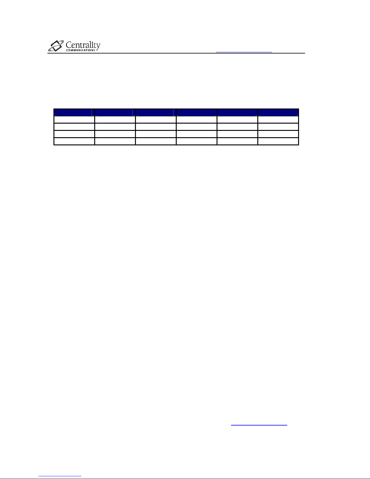
**Preliminary and Confidential under NDA, DO NOT DISTRIBUTE
Atlas™ Programming Guide **Preliminary and Confidential under NDA, DO NOT DISTRIBUTE
- 63 -
8.2 DMA Channel Sharing
The DMA channel 6, 7 & 9, 10 are shared between the four Universal Serial Ports and the Audio
CODEC. The following table shows the DMA channel multiplex managed by RSC:
Table 8. Atlas™ DMA Channel Multiplex
USP0 USP1 USP2 USP3 CODEC
DMA Ch6
- - - Yes Yes
DMA Ch7
- - - Yes Yes
DMA Ch9
Yes Yes Yes Yes -
DMA Ch10
Yes Yes Yes Yes -
By default DMA Channel 6&7 are occupied by CODEC, and Channel 9&10 are occupied by USP0.
When other USP needs to use DMA, it needs to change the RSC_DMA_MUX register as following:
RSC_DMA_MUX = 0x3C // USP3 occupy DMA channel 6&7
The reason why USP3 may needs at most 4 DMA channels is: the USP3 has a special SIB bus mode,
which the other USP’s do not have. In this mode, there are both Audio data and Telecommunication data
need to be transferred in the same frame. And both data transfers are bi-directional.
NOTE: Please make sure the related DMA channels are in idle state when programming this
register.
Page 65
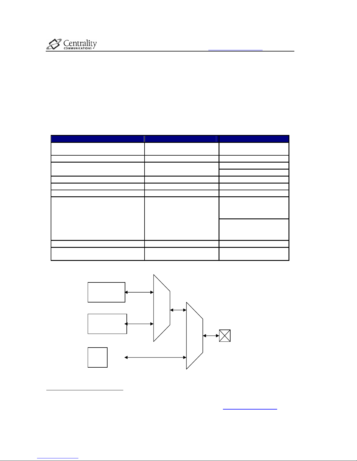
**Preliminary and Confidential under NDA, DO NOT DISTRIBUTE
Atlas™ Programming Guide **Preliminary and Confidential under NDA, DO NOT DISTRIBUTE
- 64 -
8.3 External Pin Multiplex
After power-on reset of boot-up, the Resource Sharing Controller controls all the peripheral pins. In this
mode, the input/output or pull-up/down status of each pin is fully programmable. Only after the
PWR_PIN_RELEASE register in the Power Manager was set, those pins can released to each
peripherals. If the pin is multiplexed between more than two functions, by default the pins are released to
the first function peripheral. User can switch the pins to the second (or third) function by configuring the
RSC register RSC_PIN_MUX. The Atlas™ multiplexed pins managed by the RSC are shown in the next
table (the memory interface pin multiplex is not managed by RSC):
Table 9. Atlas™ Pin Multiplex
Pads First Function Second Function
A1, A2, A3, A4, A5, B1, B2, B3, B4,
B5, C2, C3, C4
SmartMedia®/NAND Flash
interface
CMOS/CCD Sensor
H1, H2, H5, J1, J2, J3, J5, K3
GPIO<15:8> LCD controller
Serial Port 0
N3, N5, P5
GPIO<23:21>
TIC
P1, P2, P3, R3
Serial Port 1 Audio CODEC
R1, T1, T3, U1
Serial Port 2 Bluetooth SPI
U5, U6, V5, W4, W5
GPIO<20:16> JTAG
Host port
K18, K19, L15, L17, L18, M18, M19,
P10, P11, P12, P13, P14, R17, R18,
T17, T18, T19, U10, U11, U12, U13,
U14, U15, U16, U17, U18, U19, V10,
V11, V12, V13, V14, V15, V16, V17,
V18, V19, W10, W11, W12, W13,
W14, W15, W16, W17, W18, W19
PCMCIA interface
Extension port
M17, N15, N17, N18, N19, P15
PCMCIA interface SD interface
A6, B6, C51, C6
NOR Flash/ROM interface
SmartMedia®/NAND Flash
interface
The following figure shows how the Atlas™ pins are multpiexed:
Figure 8. Atlas™ Pin Multiplex Diagram
1
If NAND_BOOT=1, then the C5 will be used by SmartMedia®/NAND Flash interface first.
1st Function
2nd Function
RSC
PAD
Page 66

**Preliminary and Confidential under NDA, DO NOT DISTRIBUTE
Atlas™ Programming Guide **Preliminary and Confidential under NDA, DO NOT DISTRIBUTE
- 65 -
Basically each bit in RSC_PIN_MUX register controls the multiplex of two groups of pins. But there are
some special cases:
1. Some pins are used for TIC/BIST
1
, JTAG, or Scan chain test besides of the functions listed
above. Among those functions, the TIC/BIST, JTAG, or Scan chain has the highest priority.
When Atlas™ is configured to those special test modes, those pins cannot be used by the
normal functions any more.
2. Host Port and Extension port are all shared pin with PCMCIA interface. So bit<3> and <4>
should be set to 1’b1 at the same time. But if user writes 1’b1 to both two bits, the bit<4>
(HOST_EN) has higher priority than bit<3> (EXT_EN). In another words, if bit<4> is set to 1’b1,
then Host Port will occupy those pins no matter bit<3> is 1’b1 or 1’b0.
Besides, the RSC_PIN_MUX and PWR_PIN_RELEASE register have to work together with the
PWR_CLK_EN register to decide the pin multiplex. If user wants the pins to be enabled for a dedicated
block, then he needs to enable the clock of that block too. Otherwise, the pins are still controlled by
Resource Sharing Controller. For example, to enable the pins for Camera port:
// set PIN_RELEASE
PWR_PIN_RELEASE = 1;
// enable Camera clock
PWR_CLK_EN |= 0x80;
// enable Camera port
RSC_PIN_MUX |= 0x400;
NOTE: On the other side, if the block is not using pins, then please turn off its clock. Otherwise, it
will still consuming power and unkown result may occur.
1
TIC is the abbreviation of Test Interface Controller, which is for testing ARM922T.
Page 67

**Preliminary and Confidential under NDA, DO NOT DISTRIBUTE
Atlas™ Programming Guide **Preliminary and Confidential under NDA, DO NOT DISTRIBUTE
- 66 -
9 DMA Controller
9.1 Operation Overview
The DMA controller consists of 12 independent DMA channels. Each channel can be programmed to
execute certain DMA operations independently.
The DMA transfer can be in single mode or burst mode. In single mode, each data transfer is only 1DWORD. But in burst mode, each data transfer will be 4-DWORD long.
According to the DMA addressing modes, the DMA operations can be divided into 1-D and 2-D
operations. The 2-D operation mode is more suitable for image processing (like Camera) applications.
Normally DMA has a start address and length. When the specified number of data is transferred, the
DMA will stop. But there are some applications need to transfer data to a specified memory area
repeatedly without stop (like Audio). So Atlas™ DMA Controller has a special loop mode for this type of
applications.
Page 68

**Preliminary and Confidential under NDA, DO NOT DISTRIBUTE
Atlas™ Programming Guide **Preliminary and Confidential under NDA, DO NOT DISTRIBUTE
- 67 -
9.2 Initialization
In order to setup a DMA, the programmer needs to know a few things:
1) Is this a read from memory or write to memory?
2) Where to get the data?
3) Where to put the data?
4) How to get the data (i.e. consecutively, or with jumps in between)?
5) What is the priority of this transfer?
These parameters are defined by a series of registers that the programmer must set in order to setup a
DMA properly. Each of the channels listed above has its own registers, which means that DMA’s for
different channels can co-exist at the same time. Each set of the registers defines the following values
(Note: registers for DMA channel 0 is used as an example here. All the channels have the same register
definitions):
• Starting Address – This is a 25-bit address that defines the starting address of the DMA transfer in
System Memory (i.e. either SDRAM or SRAM). If SRAM is used, then the top bits are ignored. The
starting address is defined in register: DMA_CH0_ADDR (Note: DMA_CH0_ADDR1 will trigger the
start of a DMA and must be set AFTER all the other registers). The Starting Address is a DWORD
address.
• X value – This is a 16-bit value which defines how many consecutive DWORDs to access per line of
DMA. This value is in the register DMA_CH0_XLEN.
• Y value – This a 16-bit value which defines how many lines of DMA to perform. The actual line
number of DMA is Y+1. For example, to DMA one line, Y = 0; to DMA 10 lines, Y = 9. This value is
in register DMA_CH0_YLEN.
• DMA width – This is a 10-bit value which specifies the spacing between two lines (in DWORD). For
example, if the width = 100, X = 10, and Y = 5, then each time when the DMA gets 10th DWORD, it
will jump 90 DWORDs to reach the start of the next line. Since width registers are often fixed for a
particular application, the Palm-2 provides a set of 4 width values (DMA_WIDTH0, DMA_WIDTH1,
etc.) that can be pre-initialized. A particular DMA only needs to specify which of the 4 registers to
use in the DMA_CH0_CTRL register.
Both RISC and DSP can start the DMA. Before user starts the DMA, it needs to configure the
DMA_CH_DSP_CTRL register to determine either RISC or DSP will have the control of each DMA
channel.
Some most commonly used parameters must be set up in the initialization routine
1
. The common
parameters include:
• Width registers (DMA_WIDTH0, DMA_WIDTH1, etc)
• Interrupt enable register (DMA_INT_EN)
• Direction, mode, width selection, etc. (DMA_CHx_CTRL)
• Loop enable if needed (DMA_CH_LOOP_CTRL)
• Horizontal length (DMA_CHx_XLEN)
The Vertical length (DMA_CHx_YLEN) needs to be set up every time user wants to start a new DMA. If
user wants to start a 1-D DMA, then this register does not need to be set up.
Besides of the above register set up, user also needs to set up some peripheral FIFO parameters such
as:
1
Some of these registers have defaults values that can already be used.
Page 69

**Preliminary and Confidential under NDA, DO NOT DISTRIBUTE
Atlas™ Programming Guide **Preliminary and Confidential under NDA, DO NOT DISTRIBUTE
- 68 -
• DMA or I/O mode selection
• Bit width selection (byte/word/dword)
• FIFO request level
• FIFO interrupt threshold
As for the detail about the FIFO initialization, please refer to the section describes peripheral FIFO.
To start the DMA, user just needs to write to the DMA_CHx_ADDR register
1
.
Here is a simple example for 1-D DMA from SDRAM to Flash Memory (DMA channel 4) initialization:
#define BURST 1
#define DIR 1
#define WIDTH 0
#define XLEN 0x10
#define YLEN 0
#define SDRAM_ADDR 0x100000
// set dma width registers
DMA_WIDTH0 = 0x1;
DMA_WIDTH1 = 0x4;
DMA_WIDTH2 = 0x8;
DMA_WIDTH3 = 0xc;
//set dma int enable
DMA_INT_EN = DMA_CH4_INT;
//clear all dma interrupts
DMA_CH_INT = 0xffff;
//configure and start dma
DMA_CH4_CTRL = ((BURST<<3) | (DIR<<2) | WIDTH);
DMA_CH4_XLEN = XLEN;
DMA_CH4_YLEN = YLEN;
DMA_CH4_ADDR = SDRAM_ADDR;
1
Except for the loop mode (please refer to section 9.6)
Page 70

**Preliminary and Confidential under NDA, DO NOT DISTRIBUTE
Atlas™ Programming Guide **Preliminary and Confidential under NDA, DO NOT DISTRIBUTE
- 69 -
9.3 DMA Interrupt Handling
When the DMA finishes, it will generate an interrupt in the DMA_CH_INT register. So RISC or DSP can
know that this DMA is finished. Following is a simple example shows the DMA interrupt handling:
#define DMA_CH4_INT 0x10
#define DMA_MASK_TO_SDRAM 0x00
#define DMA_MASK_FROM_SDRAM 0x04
volatile int bDMAReadDone;
volatile int bDMAWriteDone;
void __irq Irq_Handler()
{
int iStatus;
iStatus = INT_PENDING;
if(iStatus & INT_MASK_DMA_CTRL)
{
if(DMA_CH_INT & DMA_CH4_INT)
{
DMA_CH_INT = DMA_CH4_INT; // clear the DMA interrupt
if((DMA_CH4_CTRL & 0x04) == DMA_MASK_TO_SDRAM)
{
bDMAWriteDone = 1;
}
if((DMA_CH4_CTRL & 0x04) == DMA_MASK_FROM_SDRAM)
{
bDMAReadDone = 1;
}
}
}
}
The interrupt handling for loop mode DMA is a little bit different. Please refer to section 9.6 for the details.
Page 71

**Preliminary and Confidential under NDA, DO NOT DISTRIBUTE
Atlas™ Programming Guide **Preliminary and Confidential under NDA, DO NOT DISTRIBUTE
- 70 -
9.4 Single and Burst DMA
As we specified before, the DMA has two data transfer modes: single and burst mode. In single transfer
mode, the DMA controller executes one 32-bit word read/write at a time; while in burst mode, 4 32-bit
words a time. The user can select the transfer mode by programming one of the register bit in
DMA_CHx_CTRL.
In burst mode, X-length should be in 16-byte boundary normally; but it’s allowed to be set to any value.
For example, if X-length = 5, then the DMA controller is actually doing 2 bursts. But in the last burst, the
DMA controller will only do one D-word data transfer to/from the peripheral. For 1-D DMA, it is not so
important because the last data transfer in the whole DMA will not affect the peripheral FIFO anyway.
But in 2-D DMA, and if X-length is not in 16-byte boundary, then the last burst of every line will only do 1
D-word data transfer. So the DMA controller will not do extra data transfer and will not affect the data
sequence in the peripheral FIFO. Please note that from the system memory’s point of view, it will still see
2 bursts on each line, i.e., the 5 D-word data transfer of each line will take 8-Dword’s memory space.
It is suggested to use burst mode DMA whenver it is possible. It can make the data transfer more
effiecient and faster.
NOTE: In burst mode, the DMA address is better to be in 16-DWORD boundary. Otherwise, the
transfer will be split into multiple single-word transfers in the system bus (Because the system
bus does not allow the non-aligned burst transfer) and the bus efficiency will be desperately low.
Page 72
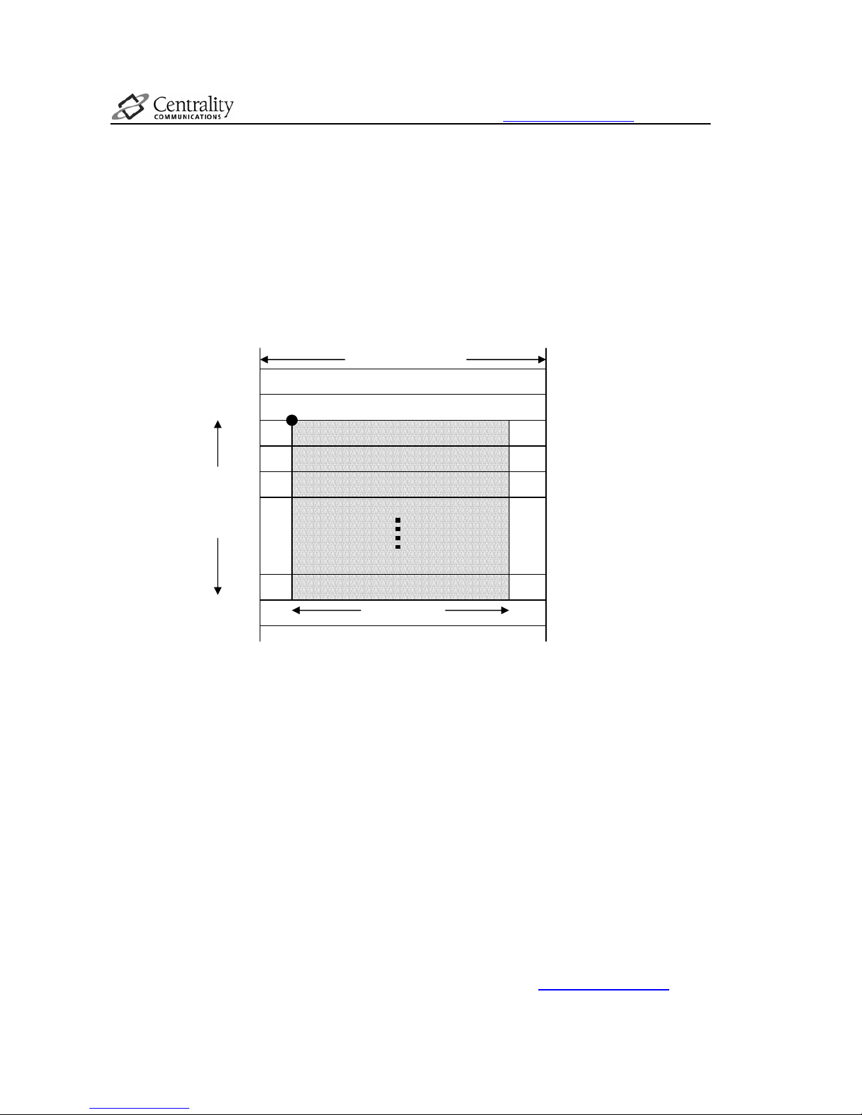
**Preliminary and Confidential under NDA, DO NOT DISTRIBUTE
Atlas™ Programming Guide **Preliminary and Confidential under NDA, DO NOT DISTRIBUTE
- 71 -
9.5 1-D and 2-D DMA
The Atlas™ DMA controller supports both 1-D and 2-D DMA. In 2-D DMA, the system memory space is
considered as a 2-D layout instead of linear layout. In another word, the system memory is considered
as many data lines. The length of the data line is determined in the user-selected DMA_WIDTH register.
Then user can specify a data window that user wants to read/write by three parameters:
• Start address
• X length
• Y length
The idea of 2-D DMA is shown in the following diagram.
Figure 9. 2-D DMA
If the user specifies the Y length as 0 or X length equals to the DMA Width, then this 2-D DMA will
actually has the same effect as 1-D DMA.
If user set up the X length greater than DMA Width, then the extra data will be wrapped around to the
next data line. It will corrupt the DMA transfer for multiple-line 2-D DMA. But if it’s 1-D DMA, then there is
no problem. The following diagram shows the wrap around of the extra data in case of X length greater
than DMA Width.
X
length
DMA Width
Y
length
Start
Address
Page 73
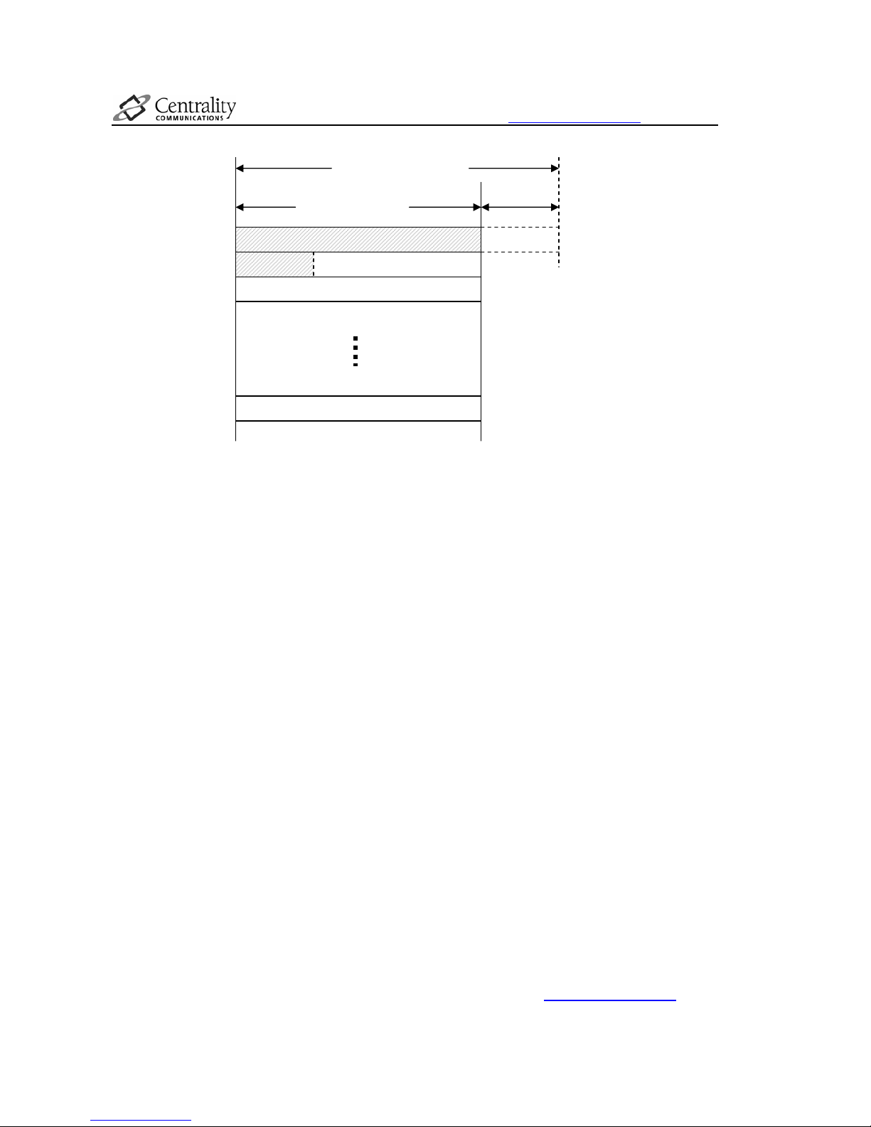
**Preliminary and Confidential under NDA, DO NOT DISTRIBUTE
Atlas™ Programming Guide **Preliminary and Confidential under NDA, DO NOT DISTRIBUTE
- 72 -
Figure 10. 2-D DMA Wrap Around (X-Length > Width)
DMA Width
DMA X-Length
Extra data
Extra data
Page 74
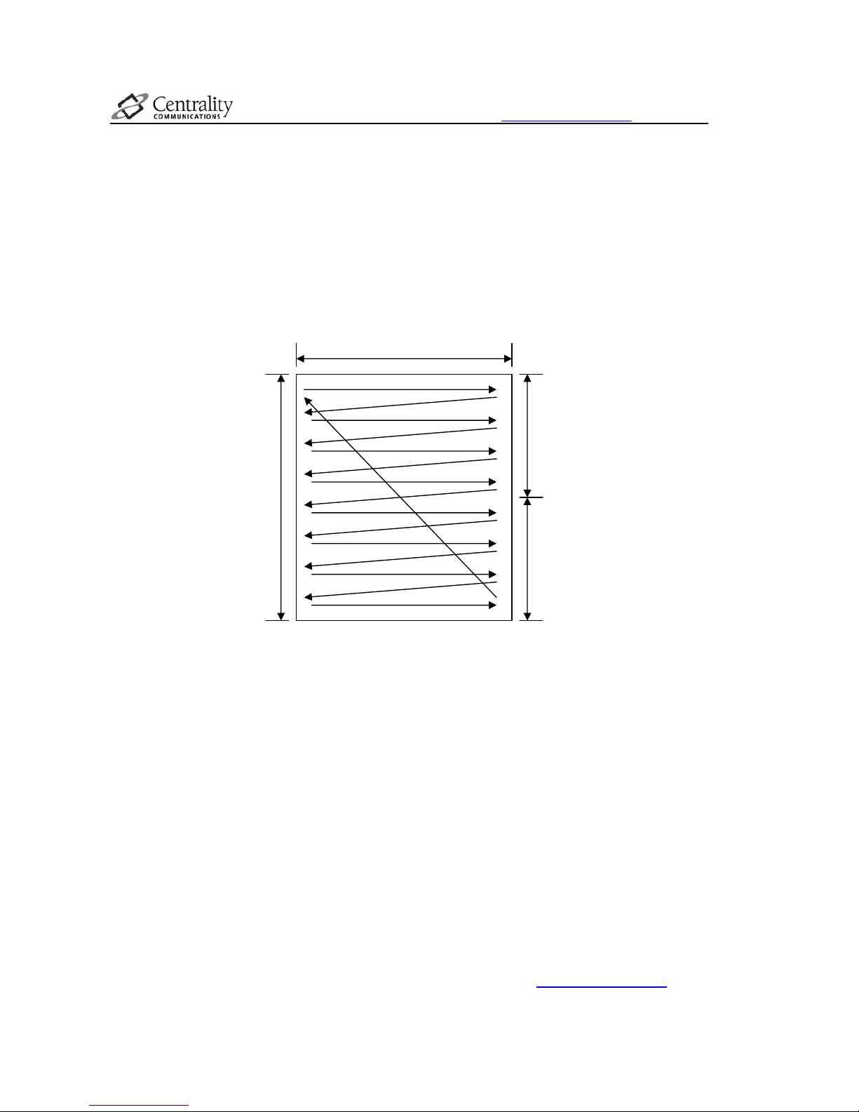
**Preliminary and Confidential under NDA, DO NOT DISTRIBUTE
Atlas™ Programming Guide **Preliminary and Confidential under NDA, DO NOT DISTRIBUTE
- 73 -
9.6 Loop DMA
If X-length is set to 0, it is a special mode of the DMA: loop mode. In loop mode, the start and stop
conditions are all different.
For loop-mode DMA, set the start address will not start the DMA at once. User needs to set the
DMA_CH_LOOP_CTRL to start the DMA. But before start a new DMA, user still needs to configure this
start address register to clear the internal status of last DMA.
The loop-mode DMA will never finish until user force to stop it (by writing a 1’b0 to the DMA_CH_VALID
register). The DMA will keep looping as described in the following figure:
Figure 11. Loop-mode DMA
As shown in the above figure, the DMA address will keep increasing, until reaching the end of a loop
area whose size is defined by (DMA_WIDTH * Y_LENGTH). Then the DMA address will go back to the
beginning of this area. If Y_LENGTH or DMA_WIDTH is equal to 0, then the DMA address will not
change at all. And the DMA will keep transferring the data to the same DMA address until user force to
stop it.
In loop mode, the DMA data region is always divided into two halves: BUFA and BUFB. The DMA
controller will generate interrupt twice during each loop: one time is when the DMA address reaches the
end of BUFA; the other time is when the DMA address reaches the end of the BUFB. And of course the
interrupt can only be generated when the corresponding interrupt enable (DMA_INT_ENABLE) bit is set.
Each half (BUFA & BUFB) has its own buffer valid register bit, which can be programmed by user. The
loop DMA will not be really started until the current buffer valid register bit is asserted. For example, if
when the DMA goes to the end of BUFA and the valid bit of BUFB is not set, then the DMA will stop at
the end of BUFA until the valid bit of BUFB is set.
Here is a simple example showing the loop DMA from SDRAM to Flash Memory:
//configure and start dma
DMA_WIDT
H
Y-LENGTH
BUFA
BUFB
Page 75

**Preliminary and Confidential under NDA, DO NOT DISTRIBUTE
Atlas™ Programming Guide **Preliminary and Confidential under NDA, DO NOT DISTRIBUTE
- 74 -
DMA_CH4_CTRL = ((BURST<<3) | (DIR<<2) | WIDTH);
DMA_CH4_XLEN = 0;
DMA_CH4_YLEN = 0;
DMA_CH4_ADDR = SDRAM_ADDR;
DMA_CH_LOOP_CTRL = 0x100010;
And the interrupt handling of the loop mode DMA is a little different with normal DMA. The following
example shows how to handle the loop mode DMA interrupt:
#define DMA_CH4_INT 0x10
#define DMA_MASK_TO_SDRAM 0x00
#define DMA_MASK_FROM_SDRAM 0x04
volatile int bDMAReadDone;
volatile int bDMAWriteDone;
void __irq Irq_Handler()
{
int iStatus;
iStatus = INT_PENDING;
if(iStatus & INT_MASK_DMA_CTRL)
{
if(DMA_CH_INT & DMA_CH4_INT)
{
DMA_CH_INT = DMA_CH4_INT ; // clear the DMA
interrupt
if((DMA_CH4_CTRL & 0x04) == DMA_MASK_TO_SDRAM)
{
bDMAWriteDone = 1;
if (DMA_CH_LOOP_CTRL & 0x10) { // if in loop
mode, swap the buffer valid
DMA_CH_LOOP_CTRL &= 0xfff0eff;
DMA_CH_LOOP_CTRL |= 0x100000;
}
else if (DMA_CH_LOOP_CTRL & 0x100000) {
DMA_CH_LOOP_CTRL &= 0xfef0fff;
DMA_CH_LOOP_CTRL |= 0x10;
}
}
if((DMA_CH4_CTRL & 0x04) == DMA_MASK_FROM_SDRAM)
{
sim_step(19);
bDMAReadDone = 1;
if (DMA_CH_LOOP_CTRL & 0x10) { // if in loop
mode, swap the buffer valid
DMA_CH_LOOP_CTRL &= 0xfff0fef;
DMA_CH_LOOP_CTRL |= 0x100000;
}
else if (DMA_CH_LOOP_CTRL & 0x100000) {
DMA_CH_LOOP_CTRL &= 0xfef0fff;
DMA_CH_LOOP_CTRL |= 0x10;
}
}
}
Page 76

**Preliminary and Confidential under NDA, DO NOT DISTRIBUTE
Atlas™ Programming Guide **Preliminary and Confidential under NDA, DO NOT DISTRIBUTE
- 75 -
}
}
To finish a loop DMA, user needs to write the DMA_CH_VALID register. For example, if user wants to
stop the DMA channel 4 which is a loop-mode DMA:
// stop loop mode DMA
DMA_CH_VALID = 0x10;
Page 77

**Preliminary and Confidential under NDA, DO NOT DISTRIBUTE
Atlas™ Programming Guide **Preliminary and Confidential under NDA, DO NOT DISTRIBUTE
- 76 -
9.7 DSP Control of DMA
By default all the DMA channels are controlled by RISC. But the RISC can set DMA_CH_DSP_CTRL
register to give some control of the DMA controller to DSP. Each DMA channel can be switch to be
controlled by RISC or DSP separately. And the switch can only be done by RISC, not DSP (i.e.
DMA_CH_DSP_CTRL is only accessible to RISC).
For example, if user wants to use DSP to control DMA channel 4:
DMA_CH_DSP_CTRL |= 0x10;
Because there might be some channels controlled by RISC and some others by DSP at the same time,
some DMA control registers need to be separated for RISC and DSP. Those registers include:
• DMA Width Registers (DMA_WIDTH0, 1, 2, 3)
• DMA Interrupt Enable Register (DMA_INT_EN)
• DMA Loop Control Register (DMA_CH_LOOP_CTRL)
Page 78

**Preliminary and Confidential under NDA, DO NOT DISTRIBUTE
Atlas™ Programming Guide **Preliminary and Confidential under NDA, DO NOT DISTRIBUTE
- 77 -
10 PCMCIA Interface
10.1 Operation Overview
Atlas
TM
PCMCIA interface is compliant with PC Card Standard 2.1, PCMCIA 2.1 and JEIDA 4.1. The
application typically access PC card through the socket/card services software interface. The PCMCIA
interface operates in 32-bit mode, even when supporting 8-bit or 16-bit PC card, PCMCIA has the logic
to route 32-bit operation to narrow bus operation. On PC card side, PCMCIA interface support Socket or
Card interrupt (activated by PC card) and Management interrupt ( invoked by PC card status change).
PCMCIA I/F also provide timing control register to accormodate interface to slower PC card or other I/O
interface.
The PCMCIA interface operation includes:
z Pin_mux programming
z M6730 Register programming
z Power logic register programming
z Memory window configuration
z I/O window configuration
z Timing control
z Management interrupt operation
z Card interrupt operation
z Card initialization sequence
Page 79

**Preliminary and Confidential under NDA, DO NOT DISTRIBUTE
Atlas™ Programming Guide **Preliminary and Confidential under NDA, DO NOT DISTRIBUTE
- 78 -
10.2 Pin-mux Programming
In Atlas
TM
there is different clock source for each peripheral for better power control, before PCMCIA
interface configuration, user needs to program the power management register to provide clock to
Atlas
tm
PCMCIA interface first; And the pin of PCMCAI interface is muxed with extension port, SD
interface and host port, by default the pin is defined for PCMCIA interface.
The pin_mux programming can access the following registers:
1. PWR_CLK_EN, see Atlas
TM
developer’s manual section 5.6.3 for details register description. Set bit
14 of PWR_CLK_EN to be 1’b1.
#define PCMCIA_CLK_EN 0x4000;
PWR_CLK_EN |= PCMCIA_CLK_EN;
2. RSC_PIN_MUX, see Atlas
TM
developer’s manual section 5.8.2 for details register description. To
make sure that bit 3 and bit 4 of register RSC_PIN_MUX is 1’b0. Since the pin of SD I/F only muxes
with PCMCIA I/F highest 6-bit address lines, when PCMCIA interface only use the lower address
bus, the SD interface pin can also be enabled.
Page 80

**Preliminary and Confidential under NDA, DO NOT DISTRIBUTE
Atlas™ Programming Guide **Preliminary and Confidential under NDA, DO NOT DISTRIBUTE
- 79 -
10.3 M6730 Register Programming
PCMCIA interface intergrates an IP core named M6730, which implements the conversion from PCI bus
to PCMCIA interface. The M6730's internal device control, window mapping, extension and timing
registers are accessed through a pair of operation registers - an index register and a data register.
Before reading/writing M6730 register, user needs to program the index register first, The index register
is used to specify which of the internal registers the CPU will access next. The data register is used by
the CPU to read and write into the internal register specified by the Index register.The M6730 also has
Extension registers. Within this Extension registers is an Extended Index register and Extended Data
register that provides access to more registers. The registers accessed through extended index and data
registers are thus double indexed.
For M6730 its base address in Atlas
TM
is fixed to be 0x2000_0000, the address for index register in
Atlas
TM
is 0x2000_0000, for data register it’s 0x2000_0001.
The order of M6730 register operation is as follows:
1. For register write operation, write index and data to base address 0x2000_0000 in word mode with
low byte is index value and high byte is data value.
#define PCMCIA_IO_PHYSICAL_BASE 0x20000000
value_short =
register_index | (((unsigned short)register_data)<<8);
*((volatile unsigned short *) PCMCIA_IO_PHYSICAL_BASE) = (unsigned
short)value_short;
2. For register read operation,
a) write index to base address 0x2000_0000 in byte mode first;
b) Read base address 0x2000_0000 in word mode;
c) Extract the high byte of read data.
*((volatile unsigned char *) PCMCIA_IO_PHYSICAL_BASE ) = (unsigned
char)register_index;
value_short = *((volatile unsigned short *) PCMCIA_IO_PHYSICAL_BASE);
register_data = (value_short & 0xFF00) >>8;
3. For extended register write operation
a) Write extended index to extended index register (0x2E)
b) Write register value to extended data register (0x2F)
value_short =
0x2E | (((unsigned short)extended_index)<<8);
*((volatile unsigned short *) PCMCIA_IO_PHYSICAL_BASE) = (unsigned
short)value_short;
value_short =
0x2F | (((unsigned short)extended_data)<<8);
*((volatile unsigned short *) PCMCIA_IO_PHYSICAL_BASE) = (unsigned
short)value_short;
4. For extended register read operation
a) Write extended index to extended index register (0x2E)
b) Read extended data register(0x2F).
value_short =
0x2E | (((unsigned short)extended_index)<<8);
Page 81

**Preliminary and Confidential under NDA, DO NOT DISTRIBUTE
Atlas™ Programming Guide **Preliminary and Confidential under NDA, DO NOT DISTRIBUTE
- 80 -
*((volatile unsigned short *) PCMCIA_IO_PHYSICAL_BASE) = (unsigned
short)value_short;
*((volatile unsigned char *) PCMCIA_IO_PHYSICAL_BASE ) = (unsigned char)
0x2F;
value_short = *((volatile unsigned short *) PCMCIA_IO_PHYSICAL_BASE);
register_data = (value_short & 0xFF00) >>8;
Page 82

**Preliminary and Confidential under NDA, DO NOT DISTRIBUTE
Atlas™ Programming Guide **Preliminary and Confidential under NDA, DO NOT DISTRIBUTE
- 81 -
10.4 Power Logic Register Programming
Atlas
TM
realizes PCMCIA power management in a different way from M6730. User needs to program
Atlas
TM
GPIO or extended GPIO to control the power supply logic and switch the power on /off. After
PCMCIA I/F detects the PC Card insertion, the power logic must be initialized before the other logic
Since the auto power scheme in M6730 doesn’t work in Atlas
TM
PCMCIA interface, the power logic
register programming should follow the steps below:
1.1 After the PCMCIA card insertion is detected, CPU reads External Data Register (extended index
0x0A) bit[1:0] to decide the VCC operating voltage supplied to PC card. The power supply selection
logic depends on hardware board design.
1.2 Set
POWER_CONTROL (index 0x2) bit 4 to indicate the Vcc power is applied to the card.
1.3 Set
POWER_CONTROL (index 0x2) bit 8 to indicate the card is enabled.
1.4 Set
EXTENSION CONTROL 1 (extended index 0x03) bit 1 to disable auto power clear bit.
Page 83

**Preliminary and Confidential under NDA, DO NOT DISTRIBUTE
Atlas™ Programming Guide **Preliminary and Confidential under NDA, DO NOT DISTRIBUTE
- 82 -
10.5 Memory Window Configuration
There are five programmable memory windows in Altas
TM
PCMCIA I/F. Those memory windows can be
configured to be attribute memory window or common memory window independently. And also the
window bus size and timing control may also be different, depending on window configuration.
When RISC accesses memory PC card, the Atlas
TM
address [31:24] is compared with Memory Upper
Address register, the address [23:12] is compared with Start Address Register and End Address
Register, if the access address is within the range of programmed memory window, M6730 will respond
to the RISC access. Also M6730 will convert the Atlas
TM
address into physical PC card address. The
Atlas
TM
address [23:12] will be added with the Offset Address Register [25:12] to get PC card address
[25:12]. The lower 12 bits just pass through of RISC address [11:0].
For example, we want a memory window located at Atlas
TM
0x24008000 with length 8K, the
corresponding physical PC card address is 0x000000, we will program:
• Memory Upper Address Register to 0x24
• Memory Start Address High Register to 0x0
• Memory Start Address Low Register to 0x08
• Memory End Address High Register to 0x0
• Memory Start Address High Register to 0x0f
• Memory offset Address High Register to 0x3f
• Memory offset Address High Register to 0xf8
Besides the window space setting, the memory window configuration includes:
- Bus size
The bus size of Memory Window is configured by setting the bit <7> of Start Address High
Register. If bit 7 is set to ‘1’, the memory window is 16-bit to PC card, if ‘0’ 8-bit size.
- Memory attribute
If bit 6 of Offset Address High Register is ‘0’, the memory window is for common memory.
If bit 6 of Offset Address High Register is ‘1’, the memory window is for attribute memory. When
attribute memory is selected, the signal “pcm_reg_b” is asserted to be LOW when the address
located between the memory window is accessed.
- Timer Select
The bit [7:6] of End Address High Register is used to select the timer set. When 2’b00, the timer
set0 is selected, otherwise the timer set1 is selected.
The memory window programming can be in the following steps:
1. Program the memory window Start Address Register, End Address Register, Upper Address
Register and Offset Address Register to decide the range of memory window.
2. Select the memory window bus size;
3. Set the memory window attribute;
4. Select the timing control register;
5. Configure the Mapping Enable Register (index 0x06) to enable the corresponding memory window.
Page 84

**Preliminary and Confidential under NDA, DO NOT DISTRIBUTE
Atlas™ Programming Guide **Preliminary and Confidential under NDA, DO NOT DISTRIBUTE
- 83 -
10.6 I/O Window Configuration
There are two I/O windows in PCMCIA interface. The PCMCIA I/O space in Atlas
TM
is 64K and ranges
from 0x2000_0000 to 0x2400_0000. Before the Atlas
TM
PCMCIA I/O address reaches to M6730
megacell, the Atlas
TM
address 0x2xxx_xxxx is converted to M6730 I/O addresss 0x0xxx_xxxx. For
M6730 megacell, the I/O address is from 0x0 to 0x400_0000. The I/O window space should be within
that space. There is no Upper Address register for I/O window. The physical address to PC card is
generated by adding M6730 I/O address with I/O Offset Address Register.
For I/O window, the configuration includes:
- I/O map address register
Include: I/O Start Address, I/O End Address, I/O Offset Address.
- Auto size
Bit 5 and Bit-1 of I/O window control register are used to set the auto size of I/O windows. Under
Auto size mode, the data size of I/O access will be decided by IOIS16_b input from PC card. When
IOIS16_b is asserted to be LOW, the data bus is 16-bit in width, if IOIS16_b is 1’b1 the data bus is
8-bit in width.
- Data Size
Bit 4 and bit 0 of I/O window control register are used to configure the data size of I/O window.
When ‘1’, the data size is 16-bit, when ‘0’ the data size is 8-bit.
- Timer select
Bit 7 and bit 3 are used to select the timer register for I/O windows. When ‘1’, Timer 1 is selected, ‘0’
Timer 0 is selected.
The I/O window configuration is in the same step as memory window.
Page 85

**Preliminary and Confidential under NDA, DO NOT DISTRIBUTE
Atlas™ Programming Guide **Preliminary and Confidential under NDA, DO NOT DISTRIBUTE
- 84 -
10.7 Timing Control
The timing of PCMCIA interface is programmable; there are two sets of timing registers. The selection of
timer is controlled by I/O window and Memory window timer control register bits. For different windows,
there is different PCMCIA interface timing.
For PC card, the timing of attribute memory is fixed as PCMCIA standard has specified. The timing of
common memory and I/O interface is decided by PCMCIA CIS information. Because the timing of
PCMCIA I/ F is programmable, besides PC card PCMCIA I/F may also be used to connect some SRAMlike variable latency I/O interface. When Atlas
TM
accesses such interface through PCMCIA I/F, the timer
register configuration and timer selection are decided by AC specification of the external device.
The timer registers include: setup timing, recovery timing and command timing.
The setup timing register controls the setup time before PC card control signals (that’s pcm_oe_b,
pcm_we_b, pcm_iord_b, pcm_iowe_b) become active. It defines the time from the assertion of
pcm_ce1_b (pcm_ce2_b or pcm_reg_b) to assertion of those control signals mentioned above.
If N
setup
is the programmed value in setup timer register, T
PCMCIA
is PCMCIA I/F internal clock period
(PCMCIA I/F internal clock is always equal to Atlas
TM
I/O clock), the setup time is:
T
setup
= 2* (N
setup
+1) * T
PCMCIA
The command timing registser controls how long the PC card active control signals will be. The data in
the command timing register represents the number of clock cycles for the active command. For timer 0
and timer 1, the default value of command timing register is 0x3 and 0x9 respectively. If N
command
is the
programmed value in command timer register, T
PCMCIA
is PCMCIA I/F internal clock period (PCMCIA I/F
internal clock is always equal to Atlas
TM
I/O clock), the command time is:
T
command
= 2* (N
command
+1) * T
PCMCIA
The recovery timing registers for each timer set controls how long a PC card cycle's recovery (that’s
pcm_oe_b, pcm_we_b, pcm_iord_b, pcm_iowe_b) time will be, in terms of the internal clock cycles. It
defines the time from the de-assertion of control signal to de-assertion of pcm_ce1_b (pcm_ce2_b or
pcm_reg_b). If N
recovery
is the programmed value in recovery timer register, T
PCMCIA
is PCMCIA I/F
internal clock period (PCMCIA I/F internal clock is always equal to Atlas
TM
I/O clock), the recovery time is:
T
recovery
= 2* (N
recovery
+1) * T
PCMCIA
The timing control register operation steps are:
1. Decide the clock cycles for setup, command and recovery timer according to AC specification of PC
card or external I/O device.
2. Select the right timer register set for corresponding window.
10.8 Management Interrupt Operation
There are four changes in the PC card status that can be programmed to cause management interrupt.
1. Card detection interrupt when card is inserted or removed;
2. Battery dead or I/O type card status change;
3. Battery warning change on the memory PC card;
4. Ready status change on the memory PC card;
Page 86

**Preliminary and Confidential under NDA, DO NOT DISTRIBUTE
Atlas™ Programming Guide **Preliminary and Confidential under NDA, DO NOT DISTRIBUTE
- 85 -
There are two interrupt modes in M6730: PCI interrupt signaling and External interrupt signaling mode.
But Atlas
TM
only supports external interrupt signaling mode, and the irq10 is assigned to M6730
management interrupt.
During initializing PCMCIA I/F, the card detect interrupt needs to be initialized. The initialization
sequence is:
1. Set bit 6 of MISC CONTRL 2 register (index is 0x1E) to enable debounce for card detect.
2. Set external interrupt mode in MISC CONTROL3 (extended register, extended index is 0x25);
3. Set bit 3 of Management Interrupt Configuration register (index 0x05) to enable card detect
interrupt.
4. Program management IRQ in Management Interrupt Configuration register, by default
management IRQ is set to be “4’hA”.
5. Clear bit4 of Interrupt And General Control Register (index 0x03) to enable M6730 mamgement
interrupt.
6. Set bit 6 of PCMCIA Interrupt Mask Register (PCMCIA I/F register, 0x0018) to enable PCMCIA
Management interrupt
7. Set bit11 of INTR_RISC_MASK register (See “Interrupt Controller” section for details) to enable
PCMCIA interrupt.
For memory type PCMCIA card, management interrupts include card detect interrupt, battery warning
interrupt, battery dead interrupt and ready status change interrupt. For I/O type PCMCIA card,
management interrupts includes card detect interrupt and card status change interrupt. For each
management interrupt, there is corresponding interrupt enable bit in Management Interrupt
Configuration, the step 3 is different for different management interrupt, all the other steps should be
same.
After the PCMCIA interrupt is triggered, the handling of management interrupt must be the following
steps:
1. Disable PCMCIA interrupt in INTR_RISC_MASK register;
2. Check Bit 7 of PCMCIA_STATUS register to see whether it’s M6730 management interrupt who
triggers the PCMCIA interrupt;
3. If Bit 7 is 1’b1, there is pending M6730 management interrupt; write 1’b1 to Bit 7 of
PCMCIA_STATUS to clear PCMCIA interrupt, then go to step 4. If Bit 7 is 1’b0, there is other
pending interrupt.
4. Read M6730 Card Status Change register (index 0x04) to judge the source of management
interrupt. The register is cleared to be 0x0 after reading.
5. If bit 3 of Card Status Change register is 1’b1, it indicates that card status changes. The Card
Status Change register indicates the source of a management interrupt generated by the M6730.
For the management interrupts to be generated, the corresponding enables should be set in the
Management Interrupt Configuration register. So is the other management interrupt.
Page 87

**Preliminary and Confidential under NDA, DO NOT DISTRIBUTE
Atlas™ Programming Guide **Preliminary and Confidential under NDA, DO NOT DISTRIBUTE
- 86 -
10.9 Card Interrupt Operation
The Socket or Card interrupt is initiated by the I/O type PC card activating the rdy/nireq signal. In Atlas
TM
we assign IRQ9 for M6730 Card interrupt and only the external signaling mode is supported.The card
interrupt is only valid for I/O type PC card. For memory type PC card, no card interrupt is generated.
The initialization of card interrupt is:
1. Set external interrupt mode in MISC CONTROL3 (extended register, extended index is 0x25);
2. Program Interrupt and General Control register (index 0x03) to set card interrupt IRQ to be 0x09;
3. Check bit5 of Interrupt and General Control register (index 0x03) to make sure that “Card is I/O” is
set.
4. Set bit 8 of PCMCIA_INTR_MASK register (PCMCIA I/F register) to enable PCMCIA card interrupt.
5. Set bit 11 of INTR_RISC_MASK register (See “Interrupt Controller” section for details) to enable
PCMCIA interrupt.
By programming Interrupt and General Control register (index 0x03) to set card interrupt IRQ to be
0x00 can clear card interrupt.
The card interrupt detect is simpler than management interrupt:
1. Disable PCMCIA interrupt in INTR_RISC_MASK register;
2. Check Bit 8 of PCMCIA_STATUS register to see whether it’s M6730 card interrupt who triggers the
PCMCIA interrupt;
3. Clear interrupt generated by PC card by accessing the PC card.
4. If Bit 8 is 1’b1, there is pending M6730 card interrupt; write 1’b1 to Bit 8 of PCMCIA_STATUS to
clear PCMCIA interrupt, then go to step 4. If Bit 8 is 1’b0, there is other pending interrupt.
Page 88

**Preliminary and Confidential under NDA, DO NOT DISTRIBUTE
Atlas™ Programming Guide **Preliminary and Confidential under NDA, DO NOT DISTRIBUTE
- 87 -
10.10 Socket Initialization Sequence
For PCMCIA interface, the socket initialization sequence is:
1. Provide clock to PCMCIA interface and enable PCMCIA pin
2. Enable card detect interrupt
3. Configure one memory window to be attribute memory windows.
4. After the card insertion is detected, program the power logic registers and provide power to PC card
(Section 10.4)
5. Read PC card CIS information to decide the card type, if I/O type PC card is detected, set
Card_is_IO is Interrupt and General Control register.
6. Allocate resource to PC card according to CIS information; configure the I/O windows or memory
windows.
7. Configre the timing registers and select the right timer for windows.
8. If I/O card is detected, enable card interrupt; if memory card is detected, enable battery warning and
other management interrupt.
PCMCIA can also connect to variable latency I/O device, when PCMCIA is used to access those device,
they are generally accessed through PCMCIA attribute memory, the steps are:
1. Provide clock to PCMCIA interface and enable PCMCIA pin
2. Program the power logic register (according to the step in section 10.4) to active the M6730
hardware logic.
3. Program the timing register according to external I/O device timing requirement.
4. Configure one memory window to be attribute memory window, the memory space is for external I/O
device.
5. Select the timer for attribute memory window.
Page 89

**Preliminary and Confidential under NDA, DO NOT DISTRIBUTE
Atlas™ Programming Guide **Preliminary and Confidential under NDA, DO NOT DISTRIBUTE
- 88 -
11 Extension port
11.1 Operation Overview
Atlas
TM
extension port supports both I/O mode and DMA mode. Extension port I/O mode is used by
Atlas
TM
to access the external I/Odevice in fixed-latency or variable latency mode. But the DMA mode is
realizeded through Atlas internal bus protocol, external glue logic is needed to implement the DMA data
transfer. Here only the I/O mode operation is described. The pin of extension port is muxed with
PCMCIA and host port.
The extension port programming includes:
1. Pin_mux programming
2. Timing register programming
3. Fixed latency access
4. Variable latency access
5. DSP access
Page 90

**Preliminary and Confidential under NDA, DO NOT DISTRIBUTE
Atlas™ Programming Guide **Preliminary and Confidential under NDA, DO NOT DISTRIBUTE
- 89 -
11.2 Pin-mux Programming
Before configure extension port, user needs to program the power management register to provide clock
to Atlas
TM
extension port interface first; and the pin of extension port interface is muxed with PCMCIA I/F
and host port, use needs to program the resource sharing register to enable the pin of extension port.
The pin_mux programming can access the following registers:
1. PWR_CLK_EN, see Atlas
TM
developer’s manual section 5.6.3 for details register description. Set bit
14 of PWR_CLK_EN to be 1’b1.
2. RSC_PIN_MUX, see Atlas
TM
developer’s manual section 5.8.2 for details register description. To
set bit 3 of register RSC_PIN_MUX.
3. INT_RISC_MASK, see Atlas
TM
developer’s manual section 2.2 for details register description. To
set bit 13 to enable extension port interrupt.
Page 91

**Preliminary and Confidential under NDA, DO NOT DISTRIBUTE
Atlas™ Programming Guide **Preliminary and Confidential under NDA, DO NOT DISTRIBUTE
- 90 -
11.3 Timing Register Programming
There are two timer registers to control the timing of extension port. The read and write operations have
two separate timer sets.
EXT_TIMER2 controls the setup and recovery time and EXT_TIMER1 controls the wait status of
extension port.
The setup register controls how many cycles there are from ext_sel_b assertion to control signals
(ext_rd_b or ext_wt_b) assertion in terms of Atlas
TM
I/O clock. The recovery timers controls the clock
cycles from control signal de-assertion to ext_sel_b (and address) de-assertion. The setup and recovery
timer registers are valid for both fixed-latency and variable latency mode.
The EXT_TIMER1 controls how many wait state cycles there are to be inserted during accessing
external I/O device. The wait state control register is only valid when extension port is configures as
internal wait state mode; in this mode, extension port can visit the fixed-latency I/O device. When
extension port works under external wait state mode, the data transfer is controlled by signal “ext_rdy_b”
asserted by external device.
If N
value
is the timer register value, T
ioclock
is the period of AtlasTM I/O clock, the time controlled by
extension port register is:
T = N
value
* T
ioclock
.
Note: The extension port timer register is onlu valid for RISC access, having no effect on DSP access.
Page 92

**Preliminary and Confidential under NDA, DO NOT DISTRIBUTE
Atlas™ Programming Guide **Preliminary and Confidential under NDA, DO NOT DISTRIBUTE
- 91 -
11.4 Fixed Latency Access
When extension port accesses the fixed latency I/O device, the configuration steps must follow:
1. Pin_mux programming according to 11.3 section.
2. Configure EXT_RISC_CTRL register to enable EXT_EN, RISC_EN, set WAIT_MODE to be internal
wait mode.
EXT_RISC_CTRL = 0x3;
3. Programe EXT_TIMER1 and EXT_TIMER2 register according to external device AC specification.
Page 93

**Preliminary and Confidential under NDA, DO NOT DISTRIBUTE
Atlas™ Programming Guide **Preliminary and Confidential under NDA, DO NOT DISTRIBUTE
- 92 -
11.5 Variable Latency Access
When extension port accesses the fixed latency I/O device, the configuration steps must follow:
1. Pin_mux programming according to 11.3 section.
2. Configure EXT_RISC_CTRL register to enable EXT_EN, RISC_EN, set WAIT_MODE to be internal
wait mode.
EXT_RISC_CTRL = 0x13;
3. Programe EXT_TIMER2 register to set setup and recovery time according to external device AC
specification.
Page 94

**Preliminary and Confidential under NDA, DO NOT DISTRIBUTE
Atlas™ Programming Guide **Preliminary and Confidential under NDA, DO NOT DISTRIBUTE
- 93 -
11.6 DSP Access
Atlas
TM
DSP can also visit external device through extension port. The timing of DSP access is
controlled by DSP interface. DSP can only access the fixed latency I/O device directly. Before DSP can
access the external device, RISC needs to initialize the extension port first:
1. Pin_mux programming to enable extension port
2. Clear bit 0 of EXT_MODE register to switch the control of extension port from RISC to DSP, allowing
DSP to access extension port. After DSP is enabled to access extension port, RISC can’t access the
other extension port register any more. RISC needs to set EXT_REG_MODE again for RISC access
of extension port registers.
Before DSP access the external device, DSP needs to initialize extension port:
1. Set DSP wait state;
2. Configure EXT_DSP_CTRL register to enable EXT_EN, DSP_EN, set WAIT_MODE to be internal
wait state.
3. If necessary, configure EXT_DSP_HI_ADDR to extend the high 8-bit address.
Page 95

**Preliminary and Confidential under NDA, DO NOT DISTRIBUTE
Atlas™ Programming Guide **Preliminary and Confidential under NDA, DO NOT DISTRIBUTE
- 94 -
12 Universal Serial Port
12.1 Operation Overview
USP is the multi-function serial interface to communicate with many common serial ports, so before
using the USP, user should make acertain that the serial interface to be connected is supported by the
USP. Please refer the developer’s manual for the detail information.
USP supports the following four kinds of serial bus,
• ASYNC serial bus (UART or IrDA)
• TFS as the the chip select or enable signal (SPI)
• TFS/RFS as the Frame synchronous signal (PCM etc)
• TFS as state machine transfer control signal of the external device (SFS of PBA313)
The different bus has the different operation steps, but the basic operation steps of the USP is the same
as following:
• Reset then power up the USP
• USP work mode1 initialization
• TX FIFO/RX FIFO configuration and initializaion
• Transmit/Receive
• …
• USP work mode2 reinitialization(if need)
• Reconfiguration (if need)
• Transmit/Receive (if need)
• …
In some application, USP must be configure to several kind of serial bus, so before the USP is used, it
need to be reconfigured to the corresponding mode.
Page 96

**Preliminary and Confidential under NDA, DO NOT DISTRIBUTE
Atlas™ Programming Guide **Preliminary and Confidential under NDA, DO NOT DISTRIBUTE
- 95 -
12.2 USP Reset and Power up
Before initializing the USP, software must first reset the USP one time, and then release the reset, and
then power up the the USP, and release the pins of USP at last. All the following sample code is for
USP0. It’s the same operation for another three USP’s. All the register bits and register name (it
indicates its I/O address) below can be refered to the Developers Manual.
PWR_CLK_EN | = SP0_EN;
RESET_SR | = SP0_RST;
RESET_SR &= SP0_RST;
PWR_PIN_RELEASE=1;
Because some pins of USP0 mux the pin with GPIO, if they are used, one more register should be set,
RSC_PIN_MUX= SP0_EN;
If USP is controlled by the DSP, RISC must first write 1 to the RISC_DSP_SEL bit of RISC/DSP Mode
Register, and then DSP can access the USP.
USP_RISC_DSP_MODE = 0x1;
Before USP0 work, clear all pending interrupts
USP0_INT_STATUS = USP_INT_MASK_ALL;
If the DMA is used for data transferring, software must enable the DMA controller
PWR_CLK_EN | = DMA_EN;
Page 97

**Preliminary and Confidential under NDA, DO NOT DISTRIBUTE
Atlas™ Programming Guide **Preliminary and Confidential under NDA, DO NOT DISTRIBUTE
- 96 -
12.3 USP Initialization
12.3.1 USP Work Mode Initialization
The USP initialization has something to do with the work mode of it. Before initializing the USP registers,
please read the relative section in the Atlas™ Developers Manual to make sure how to describe the
frame characteristics all the USP. The configuration procedure has been described in the Chapter 6.5.7
USP Frame Configuration detailedly. All the register bits decription refers to chapter 6.5.8 of the
Developers Manual. With the reference of Figure 54-58, Chapter 6.5.7-6.5.8, user can configure the
register bits to the correct work mode of USP by following the register sequence described below
12.3.1.1 USP Pin Mode Register Bits
Firstly, set all the USP pins that will be used to USP function and the rest pin can be set to I/O mode for
other usage. The default value is USP function mode.
Quick Reference
Mode Register 1
SCLK_PIN_MODE, RFS_PIN_MODE, TFS_PIN_MODE, RXD_PIN_MODE, TXD_PIN_MODE,
SCLK_IO_MODE, RFS_IO_MODE, TFS_IO_MODE, RXD_IO_MODE, TXD_IO_MODE
12.3.1.2 SCLK Related Register Bits
The following charaterisctic is the main consideration for the SCLK.
1. Synchronous/Asynchronous mode. (If it is asynchronous mode, no sclk is need)
2. SCLK slave/master mode.
3. SCLK IDLE toggle/stop mode (the IDLE state of SCLK when the serial bus frame is in the IDLE
state)
4. SCLK IDLE high/low level mode (the SCLK stop at logic 0 or logic 1 if SCLK will stop when IDLE)
5. Count the divider number from the SYSCLK according to the frequency of SCLK
6. If the SCLK is slave, decide whether the glitch-free circuit is needed to used.
All the characteristics are mapped to by the fowllowing register bits.
Quick Reference
Mode Register 1
SYNC_MODE, CLOCK_MODE, SCLK_IDLE_MODE, SCLK_IDLE_LEVEL
Mode Register 2
USP_CLK_DIVISOR
Transmit Frame Control Register
SLAVE_CLK_SAMPLE
12.3.1.3 TFS Related Register Bits
If the serial bus is not asynchronous mode, software should configure the TFS with the following
charateristic.
1. TFS slave/master mode
2. TFS active high/low level
3. TFS source mode (if TFS is master mode, it is generated by hardware and software)
4. The valid TFS length
5. The whole transmitting frame length
Configure the TFS signal by setting the following register bits related with the the TFS
Page 98

**Preliminary and Confidential under NDA, DO NOT DISTRIBUTE
Atlas™ Programming Guide **Preliminary and Confidential under NDA, DO NOT DISTRIBUTE
- 97 -
Quick Reference
Mode Register 1
TFS_ACT_LEVEL
Mode Register 2
TFS_MS_MODE, TFS_SOURCE_MODE,
Transmit Frame Control Register
TX_SYNC_LEN, TX_FRAME_LEN
12.3.1.4 TXD Related Register Bits
TXD is the transmitted data line. All the following characteristics must be considered and set.
1. TX data is driven by the rising/falling edge of SCLK if serial bus is synchronous mode.
2. TX data is MSB/LSB on the data line
3. TX data length in one transmitted frame
4. TX data delay length after TFS is valid or frame starts
5. TX data shifter length when transmitting
6. the last data/zero is sent out repeatedly if the underflow happens
All the characteristics above are mapped to by the fowllowing register bits.
Quick Reference
Mode Register 1
TXD_ACT_EDGE, ENDIAN_CTRL, TX_UFLOW_REPEAT
Mode Register 2
TXD_DELAY_LEN
Transmit Frame Control Register
TX_DATA_LEN TX_SHIFTER_LEN
12.3.1.5 RFS Related Register Bits
Receiving operation shares the one frame synchronous signal with the transmiting usually, but in some
application, especially in the RFS slave mode, they use the different ones. So in these cases, software
must still configure the RFS by the following characteristics
1. RFS slave/master mode
2. RFS active high/low level
3. the whole receving frame length
Configure the RFS signal by setting the following register bits related with the the RFS.
Quick Reference
Mode Register 1
RFS_ACT_LEVEL
Mode Register 2
RFS_MS_MODE
Receive Frame Control Register
RX_FRAME_LEN
12.3.1.6 RXD Related Register Bits
RXD is the received data line. All the following characteristics must be considered and set.
1. RX data is driven by the rising/falling edge of SCLK if serial bus is synchronous mode.
2. RX data length in one receiving frame
3. RX data delay length after RFS/TFS is valid or frame starts
4. RX data shifter length when receiving
All the characteristics above are mapped to by the fowllowing register bits.
Page 99

**Preliminary and Confidential under NDA, DO NOT DISTRIBUTE
Atlas™ Programming Guide **Preliminary and Confidential under NDA, DO NOT DISTRIBUTE
- 98 -
Configure the RXD signal by setting the following register bits related with the the RXD.
Quick Reference
Mode Register 1
RXD_ACT_EDGE
Mode Register 2
RXD_DELAY_LEN
Receive Frame Control Register
RX_DATA_LEN, TX_SHIFTER_LEN
12.3.1.7 Other Frame Setting Related Register Bits
Till now, software has configured most mode setting register bits, but some other more register still need
to setting to configure the frame completely.
If the current USP is set to IrDA mode, those register bits below must be set:
• IrDA related register bits
Quick Reference
Mode Register 1
HPSIR_EN, IRDA_WIDTH_DIV, IrDA_IDLE_LEVEL
Mode Register 2
IRDA_DATA_WIDTH
Software needs to enable all the interrupt that it is used by setting the Interrrupted enable register
• Interrupted related register bits
The last two registers bits are showed below. They are very important for controlling the transmit/receive
operation sequency and continuity. Software can make the transmitting and receiving happen in the
same frame or different frame, simultenuously or alternatively, etc.
• TX/RX work mode related register bits
Quick Reference
Mode Register 2
ENA_CTRL_MODE, FRAME_CTRL_MODE
Till now you have finished configure all the registers related the transmitting/receiving frame. Thereafter
you must configure the TX FIFO/RX FIFO related register bits to make them work rightly.
12.3.1.8 TX FIFO/RX FIFO related register bits
You must first set the DMA I/O MODE register of both TX FIFO and RX FIFO to decide whether the DMA
or IO control the data transmitting/receiving.
After that, the data length of transmitting/receiving must be set.
Then you must set the FIFO_WIDTH bit in the (TX_FIFO/RX_FIFO) control register to decide
exchange a byte/word/dowrd data with the FIFO. If the DMA mode is select, FIFO_WIDTH must be set
to 0x2.
Page 100

**Preliminary and Confidential under NDA, DO NOT DISTRIBUTE
Atlas™ Programming Guide **Preliminary and Confidential under NDA, DO NOT DISTRIBUTE
- 99 -
If DMA mode is used, one more register, USP TX_FIFO level check register, must be set to decide
when to apply the DMA request for the TX_FIFO/RX_FIFO.
Quick Reference
TX FIFO related registers:
USP TX_FIFO DMA I/O MODE register
USP TX_FIFO DMA I/O length register
USP TX_FIFO control register
USP TX_FIFO operation register
USP TX_FIFO status register
RX FIFO related registers:
USP RX_FIFO DMA I/O MODE register
USP RX_FIFO DMA I/O length register
USP RX_FIFO control register
USP RX_FIFO operation register
USP RX_FIFO status register
After finishing all the register setting, software must reset and start the TX_FIFO and RX_FIFO, and then
set the USP_EN bit of the register USP0_MODE1 to enable USP transmit and receive hardware logic
After configuration of USP, enable the USP transmit and receiving logic by setting the USP_EN bit in
register of USP_MODE1.
// fifo Start
USP0_TXFIFO_OP = 0x1;
USP0_RXFIFO_OP = 0x1;
// fifo Start
USP0_TXFIFO_OP = 0x2;
USP0_RXFIFO_OP = 0x2;
//enable all the transmit and receive logic
USP0_MODE1 |= 0x20;
12.3.2 Sample Code of USP Initialization
Have known the key factor of each pin signal of USP and the frame description, here the initialization of
some kind of serial bus is introduced below.
The function of following sample code is initialization of the USP to the corresponding work mode. Each
section is for a kind of serial bus. All the sample code below is initialized to IO mode for both TX_FIFO
and RX_FIFO.
12.3.2.1 Uart Mode Initial
The following code is for 1 start bit 8 data bit, 1 stop bit, and without parity bit.
Because there is some state transfer on the TXD, in order to avoid the influence of it to the other device,
TXD should first be set to I/O output mode and output logic 1 to it. After finishing all the initialization, set
the TXD to USP function again.
#define USP_LITTLE_ENDIAN 0x10
#define USP_TXD_AS_GPIO 0x10000
#define USP_TX_IO_MODE 0x1
#define USP_RX_IO_MODE 0x1
#define USP_ENABLE 0x20
// count the clock divider
usp_baud_rate = (IO_CLOCK/8/baudrate + 1)/2-1;
 Loading...