

Central Engineering CE8301 User Manual
SMALL PACKAGE PFM CONTROL STEP-UP DC/DC CONVERTER CE8301 Series
SMALL PACKAGE PFM CONTROL
STEP-UP DC/DC CONVERTER
CE8301 Series
Introduction
The CE8301 Series is a CMOS PFM-control
step-up switching DC/DC converter that
mainly consists of a reference voltage
source, an oscillator, and a comparator. The
PFM controller allows the duty ratio to be
automatically switched according to the load
(light load: 50%, high output current: 75%),
enabling products with a low ripple over a
wide range, high efficiency, and high output
current. With the CE8301 Series, a step-up
switching DC/DC converter can be
configured by using an external coil,
capacitor, and diode. The built-in MOS FET is
turned off by a protection circuit when the
voltage at the LX pin exceeds the limit to
prevent it from being damaged. This feature,
Features
• Low voltage operation: Startup at 0.9 V
min. (I
• Duty ratio: 66/78%, builtin auto switching
type PFM controller
• External parts: Coil, capacitor, diode
• Output voltage: Settable to between 1.8
to 6.5 V in 0.1 V steps
• Accuracy of ±2%
• High efficiency:85%(typ.)
• Standard function (product type A)
• Shutdown function (product type C、D)
• Output voltage Adjustable type (product
= 1 mA) guaranteed
OUT
along with the mini package and low current
consumption, makes the CE8301 Series
ideal for applications such as the power
supply unit of portable equipment.
Applications
• Power supply for portable equipment such
as digital cameras, electronic notebooks, and
PDAs
• Power supply for audio equipment such as
portable CD/MD players
• Constant voltage power supply for cameras,
video equipment, and communications
equipment
type E、F)
• External transistor type available
(product type B、 E、F)
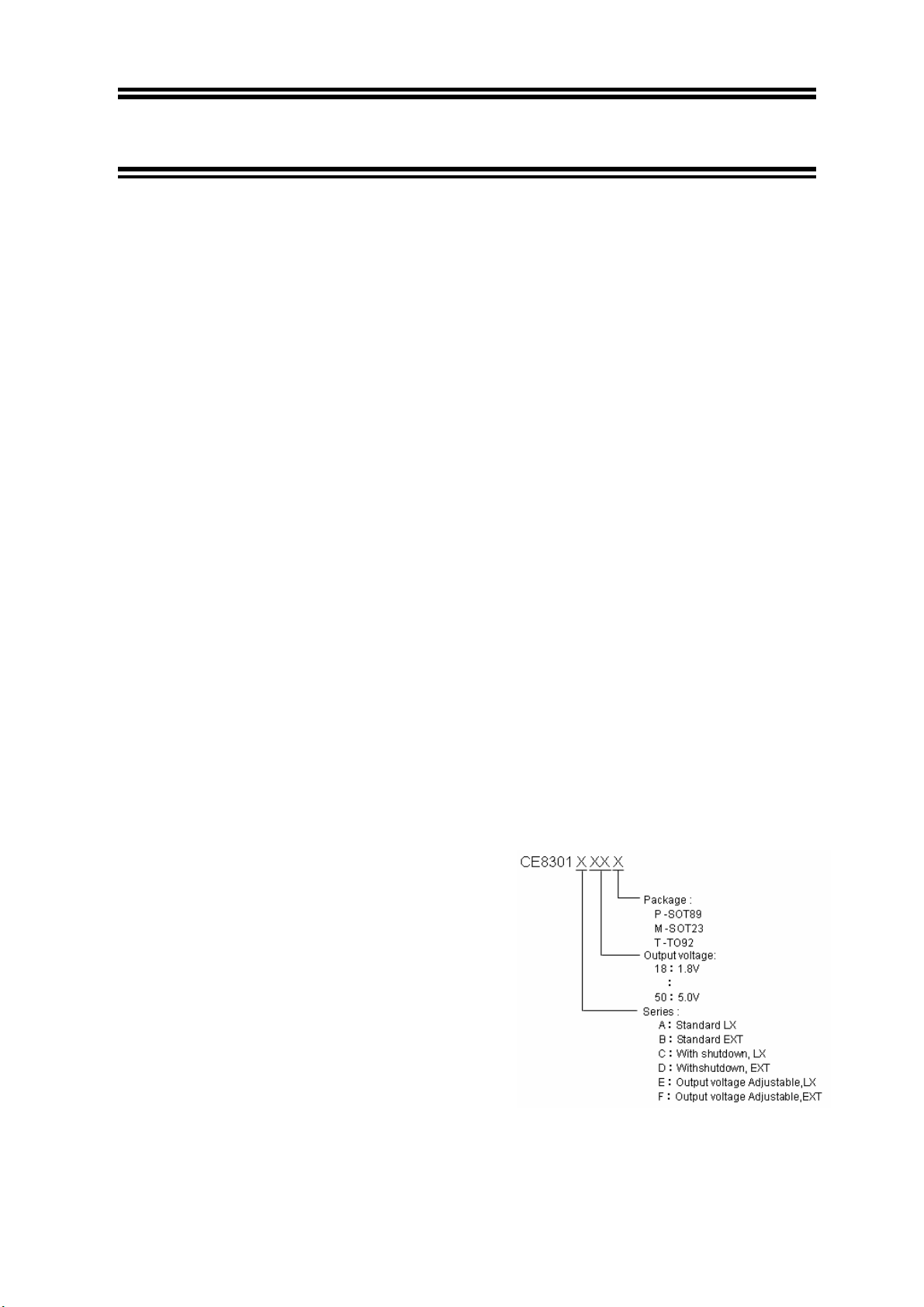
Ordering Information
• Power supply for microcomputers
SMALL PACKAGE PFM CONTROL STEP-UP DC/DC CONVERTER CE8301 Series
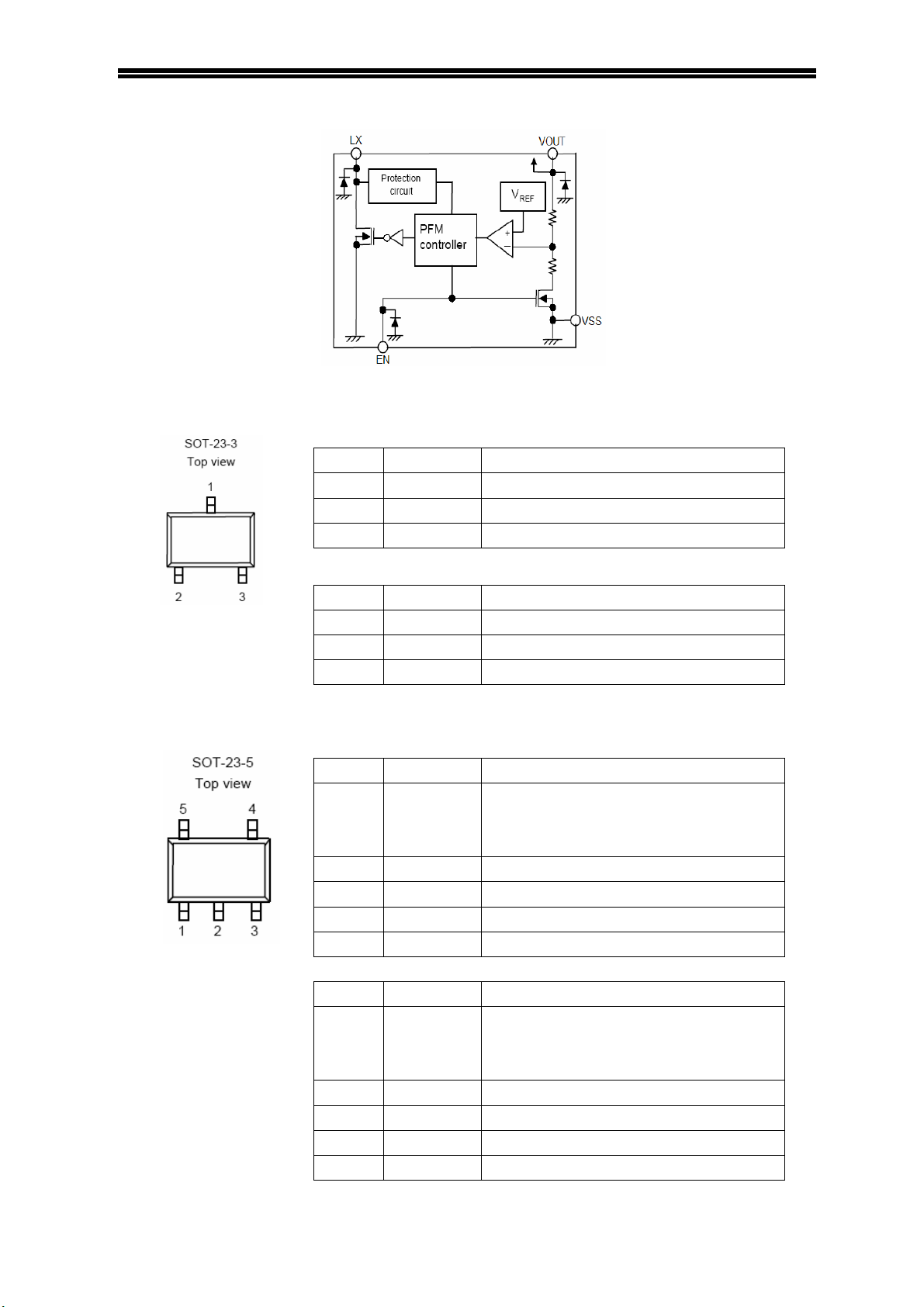
Block Diagrams
Pin Assignment
Table 1 CE8301A Series(SOT-23-3 PKG)
Pin No.
1 V
Pin Name
Output voltage pin
OUT
Functions
2 VSS GND pin
3 LX External inductor connection pin
Table 2 CE8301B Series(SOT-23-3 PKG)
Pin No.
1 V
Pin Name
Output voltage pin
OUT
Functions
2 VSS GND pin
3 EXT External transistor connection pin
Table 3 CE8301C Series(SOT-23-5 PKG)
Pin No.
Pin Name
Functions
Shutdown pin
1 EN
“H”: Normal operation
“L”: Step-up stopped
2 V
Output voltage pin
OUT
3 NC (N.C.)
4 VSS GND pin
5 LX External transistor connection pin
Table 4 CE8301D Series(SOT-23-5 PKG)
Pin No.
Pin Name
Functions
Shutdown pin
1 EN
“H”: Normal operation
“L”: Step-up stopped
2 V
Output voltage pin
OUT
3 NC (N.C.)
4 VSS GND pin
5 EXT External transistor connection pin
SMALL PACKAGE PFM CONTROL STEP-UP DC/DC CONVERTER CE8301 Series
Table 5 CE8301 ESeries(SOT-23-5 PKG)
Pin No.
Pin Name
Functions
Output voltage fixed output type;
1
VOUT
(FB)
Output voltage monitoring pin
(Output voltage external setting type;
Feedback pin)
2 VDD IC power supply pin
3 NC (N.C.)
4 VSS GND pin
5 LX External transistor connection pin
Table 6 CE8301 FSeries(SOT-23-5 PKG)
Pin No.
Pin Name
Functions
Output voltage fixed output type;
1
VOUT
(FB)
Output voltage monitoring pin
(Output voltage external setting type;
Feedback pin)
2 VDD IC power supply pin
3 NC (N.C.)
4 VSS GND pin
5 EXT External transistor connection pin
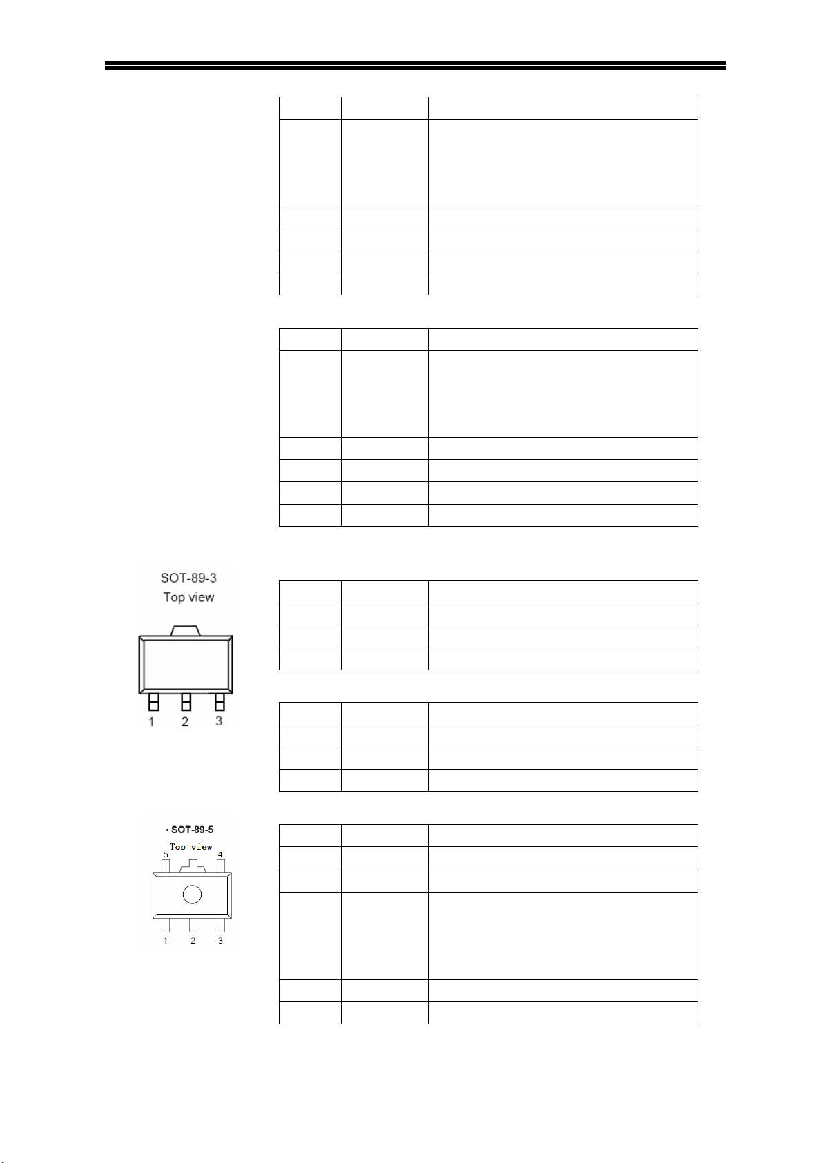
Table 7 CE8301A Series (SOT-89-3 PKG)
Pin No.
Pin Name
Functions
1 VSS GND pin
2 V
Output voltage pin
OUT
3 LX External inductor connection pin
Table 8 CE8301B Series (SOT-89-3 PKG)
Pin No.
Pin Name
Functions
1 VSS GND pin
2 V
Output voltage pin
OUT
3 EXT External transistor connection pin
Table 9 CE8301E Series (SOT-89-5 PKG)
Pin No.
1 NC
Pin Name
Functions
(N.C.)
2 VDD IC power supply pin
Output voltage fixed output type;
3
VOUT
(FB)
Output voltage monitoring pin
(Output voltage external setting type;
Feedback pin)
4 LX External transistor connection pin
5 VSS GND pin
Table 10 CE8301F Series(SOT-89-5 PKG)
SMALL PACKAGE PFM CONTROL STEP-UP DC/DC CONVERTER CE8301 Series
Pin No.
1 NC
Pin Name
Functions
(N.C.)
2 VDD IC power supply pin
Output voltage fixed output type;
3
VOUT
(FB)
Output voltage monitoring pin
(Output voltage external setting type;
Feedback pin)
4 EXT External transistor connection pin
5 VSS GND pin
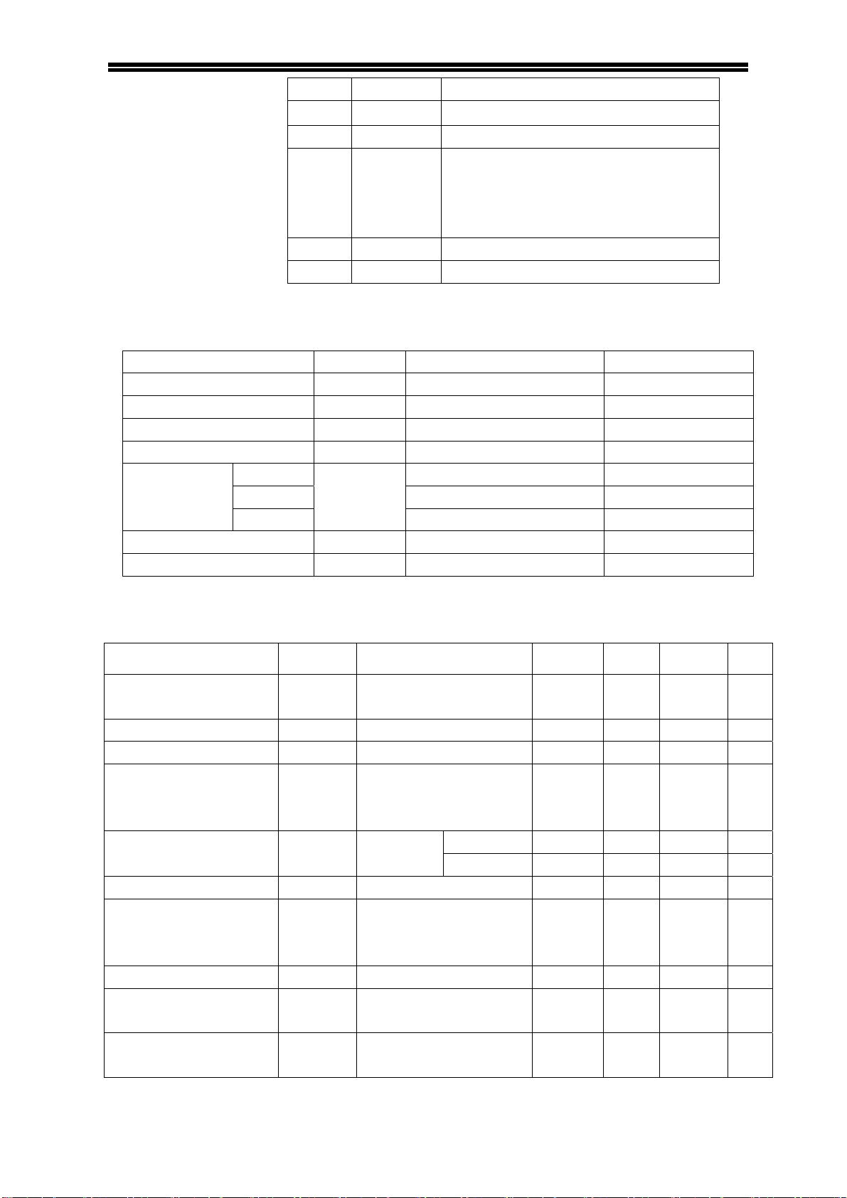
Absolute Maximum Ratings
(Unless otherwise specified, Ta=25 C)
Parameter Symbol Ratings Unit
VOUT pin voltage V
EN pin voltage EN
LX pin voltage VLX
OUT
-0.3 ~ VSS+10
V
SS
-0.3 ~ VSS+10
V
SS
-0.3 ~ VSS+10
V
SS
V
V
V
LX pin current ILX 1000 mA
Power
dissipation
Operating temperature Topr
Storage temperature Tstg
SOT-23-3 250 mW
SOT-23-5 250 mW
SOT-89-3
PD
500 mW
-40 ~+85
-40 ~+125
°C
°C
Electrical Characteristics
(Unless otherwise specified, Ta =25 C)
Parameter Symbol Conditions Min. Typ. Max. Unit
V
Output voltage V
OUT
Input voltage VIN
Operation start voltage V
Oscillation start voltage V
Current consumption 1 I
Current consumption 2 I
ST1
ST2
SS1
SS2
I
= 1 mA
OUT
No external parts, voltage
applied to V
to V
via 300 resistor
OUT
=0.95
V
OUT
×V
OUT
V
OUT=VOUT
-
- - -
LX pulled up
OUT
V
:3.0V -
OUT
V
:5.0V
OUT
+0.5 V -
OUT(S)
×0.98
V
OUT
- -
- -
30 40 µA
50 60 µA
6 10 µA
Current consumption
during
VEN = 0 V
I
SSS
- -
shutdown
Switching current ISW VLX= 0.4 V 100 200
Switching transistor
leakage current
Line regulation V
I
SWQ
OUT1
No external parts,
V
LX=VOUT
V
= 0.4×V
IN
0.6×V
=10 V ,VEN = 0 V
~
OUT
OUT
- -
-
20 50 mV
V
×1.02
OUT(S)
V
10 V
0.9 V
0.8 V
0.5 µA
-
mA
0.5 µA
 Loading...