

CENTR CMPF4393, CMPF4392, CMPF4391 Datasheet
CMPF4391
CMPF4392
CMPF4393
CentralCentral
Central
CentralCentral
Semiconductor Corp.Semiconductor Corp.
Semiconductor Corp.
Semiconductor Corp.Semiconductor Corp.
TM
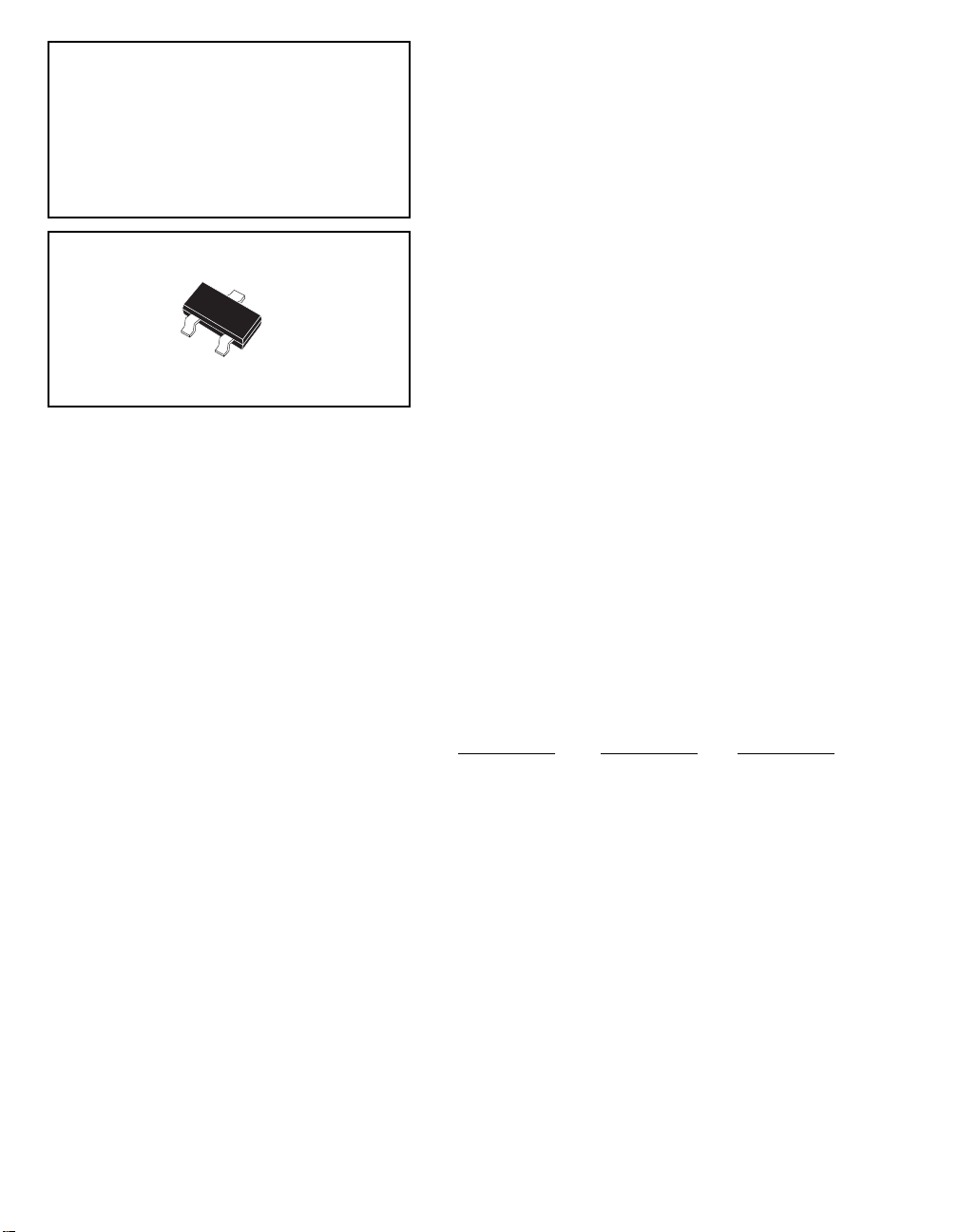
N-CHANNEL JFET
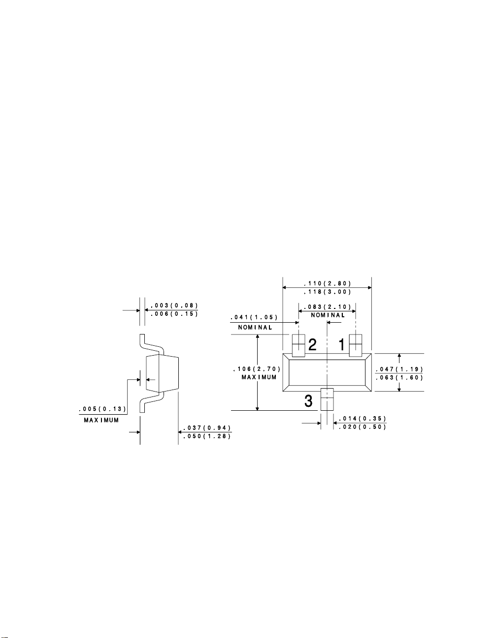
SOT-23 CASE
MAXIMUM RATINGS (TA=25oC)
SYMBOL UNITS
Drain-Gate Voltage V
Gate-Source Voltage V
Drain-Source Voltage V
Gate Current I
Power Dissipation P
Operating and Storage
Junction Temperature TJ,T
Thermal Resistance Θ
ELECTRICAL CHARACTERISTICS (TA=25oC unless otherwise noted)
GD
GS
DS
G
D
stg
JA
DESCRIPTION:
The CENTRAL SEMICONDUCTOR
CMPF4391 series types are N-Channel Silicon
Field Effect Transistors manufactured by the
epitaxial planar process, epoxy molded in a
surface mount package, designed for switching
applications.
Marking Codes are 6J, 6K, and 6G
Respectively.
40 V
40 V
40 V
50 mA
350 mW
-65 to +150
357 oC/W
o
C
CMPF4391 CMPF4392 CMPF4393
SYMBOL TEST CONDITIONS MIN MAX MIN MAX MIN MAX UNITS
I
GSS
I
GSS
I
DSS
I
D(OFF)
I
D(OFF) VDS
I
D(OFF)
I
D(OFF)
I
D(OFF)
I
D(OFF)
BV
V
V
V
V
V
VGS=20V 0.1 0.1 0.1 nA
VGS=20V, TA=100oC 0.2 0.2 0.2 µA
VDS=20V 50 150 25 75 5.0 30 mA
VDS=20V, VGS=12V 0.1 - - nA
=20V, VGS=7.0V - 0.1 - nA
VDS=20V, VGS=5.0V - - 0.1 nA
VDS=20V, VGS=12V,TA=100oC 0.2 - - µA
VDS=20V, VGS=7.0V, TA=100oC - 0.2 - µA
VDS=20V, VGS=5.0V, TA=100oC - - 0.2 µA
GSS IG
GS(OFF) VDS
IG=1.0mA 1.0 1.0 1.0 V
GS(f)
DS(ON)
DS(ON)
DS(ON)
=1.0µA 40 40 40 V
=20V, ID=1.0nA 4.0 10 2.0 5.0 0.5 3.0 V
ID=12mA 0.4 - - V
ID=6.0mA - 0.4 - V
ID=3.0mA - - 0.4 V
146
CMPF4391 CMPF4392 CMPF4393
SYMBOL TEST CONDITIONS MIN MAX MIN MAX MIN MAX UNITS
r
DS(ON)
r
ds(ON)
C
iss
C
rss
C
rss
C
rss
t
ON
t
ON
t
ON
t
OFF
t
OFF
t
OFF
All dimensions in inches (mm).
ID=1.0mA, VGS=0 30 60 100 Ω
VGS=0, ID=0, f=1.0kHz 30 60 100 Ω
VDS=20V, VGS=0, f=1.0MHz 14 14 14 pF
VGS=12V, VDS=0, f=1.0MHz 3.5 - - pF
VGS=7.0V, VDS=0, f=1.0MHz - 3.5 - pF
VGS=5.0V, VDS=0, f=1.0MHz - - 3.5 pF
I
I
I
V
V
V
=12mA 15 - - ns
D(ON)
=6.0mA - 15 - ns
D(ON)
=3.0mA - - 15 ns
D(ON)
GS(OFF)
GS(OFF)
GS(OFF)
=12V 20 - - ns
=7.0V - 35 - ns
=5.0V - - 50 ns
LEAD CODE:
1) DRAIN
2) SOURCE
3) GATE
147
R2
 Loading...