

CELER CMM3566-LC-000T, CMM3566-LC Datasheet
3236 Scott Boulevard Santa Clara, California 95054 Phone: (408) 986-5060 Fax: (408) 986-5095
CMM3566-LC
Features
❏ 7.0V Bias Voltage
❏ +24 dBm Linear Output Power (W-CDMA)
❏ 30 dB Gain at Operating Output
❏ Tested Under Digital Modulation (W-CDMA)
❏ Leadless Chip Carrier (LCC) Package
Applications
❏ Wireless Local Loop Subscriber Units
❏ Wireless Local Loop Base Stations
Description
The CMM3566-LC is a 7.0 V, +24 dBm, linear
power amplifier intended for use in PCS handsets and wireless
local loop subscriber units and base stations. The amplifier is
biased to meet the requirements of linear modulation systems
of W-CDMA.
The CMM3566-LC is packaged in a low-cost, space
efficient, power package that provides excellent electrical stability and low thermal resistance. The part requires minimal
external circuitry for bias and matching to reduce space and
cost.
3.45 to 3.5 GHz
7.0V, +24 dBm
W-CDMA Power Amplifier
Preliminary Product Information
November 2000 (1 of 4)
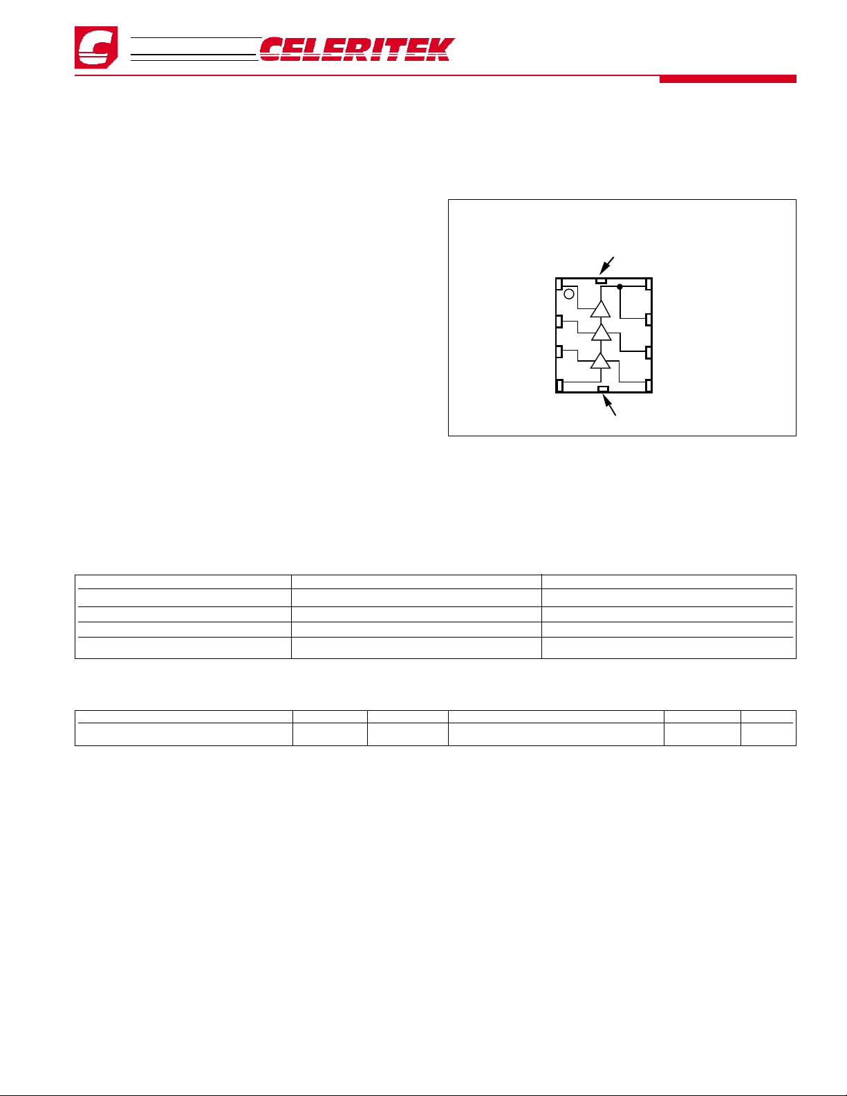
Ground Tab
Vg3 1
RF IN 4
Vg2 2
Vg1 3
7 RF OUT/+V
d3
8 RF OUT/+V
d3
5 Vd16 V
d2
Ground Tab
Functional Block Diagram
Absolute Maximum Ratings
Parameter Rating Parameter Rating Parameter Rating
Drain Voltage (+Vd) +8 V* Power Dissipation 5 W Operating Temperature -30°C to +90°C
Drain Current (Id) 1.0 A Thermal Resistance 20°C/W Channel Temperature 150°C
RF Input Power 0 dBm* Storage Temperature -65°C to +150°C Soldering Temperature 240°C for 5 Sec.
DC Gate Voltage (-Vg) -4.0 V* BV
GD
18 V
Recommended Operating Conditions
Parameter Typ Units Parameter Typ Units
Drain Voltage (+Vd) 7.0 Volts Operating Temperature (PC Board) -40 to +70 °C
* Max (+Vd) and (-Vg) under linear operation. Max potential difference across the device at 1dB gain compression point (2V
d
+ |-Vg|) not to exceed the minimum breakdown voltage (BVGD) of +18V.
Application Information
The CMM3566-LC is a three stage amplifier that requires a
positive and a negative supply voltages for proper operation. It is
essential when turning on the device that the negative supply be
applied before the positive supply. When turning the device off,
the positive supply should be removed before the negative supply
is removed.
The CMM3566-LC can be operated over a range of supply
voltages and bias currents. It is important that the maximum power
dissipation specification for the package be observed at all times
and that the maximum voltage across the device not be exceeded.
Circuit Design Considerations
Biasing Three negative voltages are needed to set the bias current
of the 3-stage GaAs FET power amplifier. The first stage bias is
controlled via Vg1. The second stage bias is controlled via Vg2.
The output stage is controlled via Vg3. The recommended divider
networks for each gate bias shown in the schematic. The positive
supply voltage is applied to pins 5, 6, 7 and 8. The negative voltage supplies control the quiescent current of the device. The quiescent current needs to be set at the level specified in order to get the
guaranteed RF performances.
Negative bias voltages can also be used to control the gain,
the output power and the operating current during operation of the
device.
Matching Circuits Output matching circuit is required to achieve
the output power and gain guaranteed. Celeritek’s recommendation for the topology of the matching circuit is shown in the
schematic diagram of the test circuit in this data sheet.
In providing both the negative and positive bias voltages, it is
important to provide adequate de-coupling between the RF signal
and the DC voltages. Inadequate de-coupling could result in low
output power, low gain or oscillation. Celeritek recommends the
bias circuits shown in the evaluation circuit .
– Continued on Page 2 –
3236 Scott Boulevard, Santa Clara, California 95054
Phone: (408) 986-5060 Fax: (408) 986-5095
CMM3566-LC
Preliminary Product Information - November
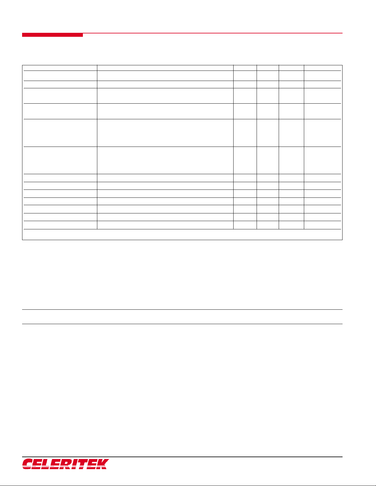
Parameter Condition Min Typ Max Units
Frequency Range 3.45 3.5 GHz
Gain @ Digital power output 26 28.5 31 dB
Gain Variation Over supply voltage 2 dB/V
Over temperature 0.03 dB/°C
Harmonics* 2nd (Pout = +22 to +26 dBm) -35 -30 dBc
3rd (Pout = +22 to +26 dBm) and above -40 -35 dBc
Linear Output Power ±2.7 MHz from carrier -43 -40 dBc/30 KHz
(Pout = +22 dBm, Data Rate = 4.096Mc/Sec
±5.25 MHz from carrier -50 -48 dBc/30 KHz
(Pout = +22 dBm, Data Rate = 4.096Mc/Sec
Linear Output Power ±2.7 MHz from carrier -38 -35 dBc/30 KHz
(Pout = +24 dBm, Data Rate = 4.096Mc/Sec
±5.25 MHz from carrier -47 -45 dBc/30 KHz
(Pout = +24 dBm, Data Rate = 4.096Mc/Sec
Wideband Noise 10 MHz Bandwidth -68 dBc
Noise Figure Vdd = 7.0 V 5 dB
Return Loss Input -10 -14 dB
Return Loss Output -10 -14 dB
Positive Supply Current (Id) Pout = +24 dBm 540 mA
Quiescent Current (Iq) No RF 520 mA
Negative Supply Current (-Ig) Includes external resistor divider 2.0 4.0 mA
Negative Supply Voltage (-Vg) Into external resistor divider -0.3 -1.5 -3.0 V
Electrical Characteristics
Unless otherwise specified, the following specifications are guaranteed at 3.45 GHz, room temperature with drain voltage (+Vd) = 7.0 V in Celeritek test fixture.
Modulation When biased as specified, the CMM3566-LC will
achieve the required adjacent channel response for the W-CDMA
linearity. Celeritek tests each product under digital modulation to
ensure compliance to system specifications.
Thermal
1. The copper pad on the backside of the CMM3566-LC must be
soldered to the ground plane.
– Continued from Page 1 –
Frequency S11 S21 S12 S22
(GHz) Mag ANG Mag ANG Mag ANG Mag ANG
0.6 0.646 136.623 2.393 20.992 0.002 -19.228 0.804 -23.817
0.8 0.659 54.979 1.283 17.015 0.003 -80.195 0.682 -89.402
1.0 0.732 -19.826 5.119 -67.405 0.004 -158.535 0.420 -138.407
1.2 0.778 -82.663 8.080 -171.314 0.005 132.866 0.382 -152.437
1.4 0.781 -140.684 10.458 93.318 0.005 67.738 0.533 150.599
1.6 0.751 155.653 12.110 -2.432 0.007 0.028 0.650 69.917
1.8 0.770 14.916 11.272 -176.757 0.006 -124.480 0.874 -61.986
2.0 0.770 11.996 11.158 -179.876 0.006 -126.766 0.880 -63.734
2.2 0.781 -40.876 11.715 106.441 0.007 173.071 0.911 -116.517
2.4 0.772 -81.765 15.438 32.091 0.008 128.121 0.877 -177.609
2.6 0.757 -121.242 21.302 -51.262 0.010 68.938 0.771 103.364
2.8 0.640 176.329 27.182 -150.627 0.011 -13.377 0.756 13.731
3.0 0.447 86.466 29.193 105.943 0.010 -79.627 0.690 -53.854
3.2 0.516 0.714 28.413 4.707 0.011 -137.593 0.471 -91.983
3.4 0.518 -69.213 25.542 -94.768 0.010 152.682 0.383 -99.415
3.6 0.131 -149.583 24.348 164.543 0.012 93.523 0.268 -121.022
3.8 0.423 -13.907 19.130 58.878 0.011 18.708 0.257 -98.953
4.0 0.578 -59.337 14.619 -37.638 0.008 -52.138 0.278 -134.978
S-Parameters
Vdd = 7V, ID 1 & 2 = 200, ID 3 = 300
* The integrity of the input signal at an offset of 5.25 MHz has an adjacent channel performance of not greater than -52 dBc.
 Loading...