

CELER CMM2308-AJ-000T, CMM2308-AJ Datasheet
3236 Scott Boulevard Santa Clara, California 95054 Phone: (408) 986-5060 Fax: (408) 986-5095
CMM2308
Features
❏ +17 dBm Output Power
❏ <2.2 dB Noise Figure
❏ Low Current: 70 mA, Typ.
❏ Single +3V to +6V Supply
❏ DC Blocked >2:1 VSWR
❏ Low-Cost SOIC-8 Plastic Package
Applications
❏ Power Amplifier Drivers
❏ PCS Medium Power Amplifiers
❏ Medium Power WLANs
❏ Base Station Receivers
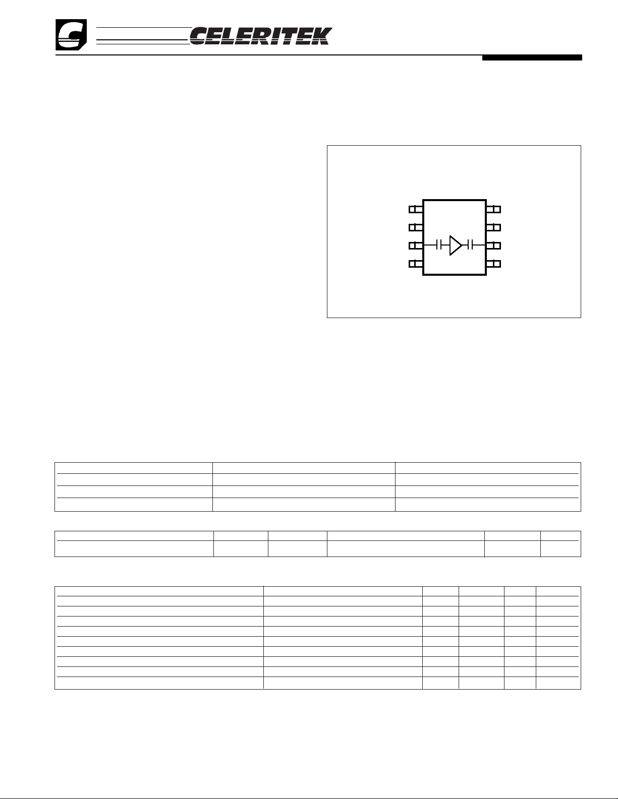
Description
The Celeritek CMM2308 is a high dynamic range,
pin-compatible, second source for the TriQuint®9132 and the
Mini-Circuits®VNA. Providing comparable gain and lower
noise figure than either of the existing standard amplifiers at
25% less drain current, the CMM2308 is an excellent choice
for power sensitive applications, while delivering more design
margin. Packaged in a low-cost surface mount SOIC-8 package, the CMM2308 will drop into existing designs and offers
improved features and performance.
Absolute Maximum Ratings
800 to 2700 MHz
High Dynamic Range Amplifier
Parameter Rating Parameter Rating Parameter Rating
Drain Voltage (+Vd) +7 V Power Dissipation 1.0 W Operating Temperature -40°C to +80°C
Drain Current (Id) 150 mA Thermal Resistance 55°C/W Channel Temperature 175°C
RF Input Power 15 dBm Storage Temperature -65°C to +150°C Soldering Temperature 260°C for 5 Sec
Recommended Operating Conditions
Parameter Typ Units Parameter Typ Units
Drain Voltage (+Vd) 3.0 to 6.0 Volts Operating Temperature (PC Board) -40 to +70 °C
Electrical Characteristics
The following specifications are guaranteed at room temperature with drain voltage (+Vd) = 5.0 V ±5% at 2.5 GHz.
Parameter Condition Min Typ Max Units
Frequency Range 800 2700 MHz
Small Signal Gain 17.5 19.0 dB
Noise Figure 1.8 to 2.5 GHz 2.2 dB
Power Output @ 1 dB Compression 15.5 17.0 dBm
Output 3rd Order Intercept 27 dBm
Input Return Loss 10 dB
Output Return Loss 10 dB
DC Supply Current 70 80 mA
Supply Voltage 35 6V
Preliminary Product Specifications
August 1996
(1 of 4)
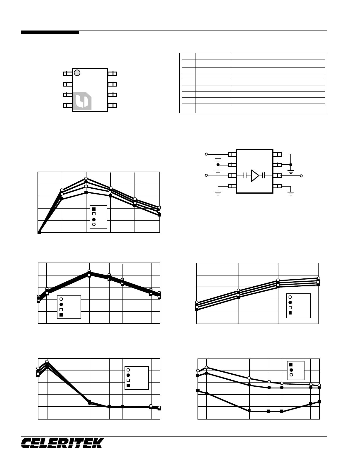
Vd 1
GND 2
RF IN 3
GND 4
8 GND
7 GND
6 RF OUT
5 GND
Functional Block Diagram
TriQuint and Mini-Circuits are trademarks of their respective corporations.
3236 Scott Boulevard, Santa Clara, California 95054
Phone: (408) 986-5060 Fax: (408) 986-5095
CMM2308
Preliminary Product Specifications - August 1996
(2 of 4)
Pin # Name Description
1 +V
d
Drain voltage. Connect to positive supply.
2 GND Ground.
3 RF IN RF input (Internally DC blocked).
4 GND Ground.
5 GND Ground.
6 RF OUT RF output (Internally DC blocked).
7 GND Ground.
8 GND Ground.
Vd 1
GND 2
RF IN 3
GND 4
8 GND
7 GND
6 RF OUT
5 GND
Connection Diagram and Pin Description
123 48765+5V
RF IN
0.01µF
RF OUT
Test Circuit Diagram
Typical Performance
The following typical performance parameters were tested in
the test circuit shown at room temperature and with a drain
voltage (+Vd) = 5 V, unless otherwise specified.
Frequency (MHz)
Gain vs Frequency vs V
d
Gain (dB)
91317212529500
1000
1500
2000
2500
3000
3V
4V
5V
6V
Frequency (MHz)
Gain vs Frequency vs Temperature @ 5V
Gain (dB)
913172125
29
-20°C
0°C
+25°C
+70°C
800
900
1500
1800
2000
2500
2400
Frequency (MHz)
Power Output (P-1) vs Frequency vs Temperature @ 5V
Power Output (P-1) (dBm)
1617181920
21
-20°C
0°C
+25°C
+70°C
800
900
1500
1800
2000
2500
2400
Frequency (MHz)
Power Output (P-1) vs Frequency vs Vd @ 25°C
Power Output (P-1) (dBm)
91215182124800
900
1500
1800
2000
2500
2400
3V
5V
6V
Supply Voltage (Vd)
Gain vs Vd vs Temperature @ 1.8 GHz
Gain (dB)
182022242628345
6
-20°C
0°C
+25°C
+70°C
 Loading...