

CELER CMM2032-BD Datasheet
3236 Scott Boulevard Santa Clara, California 95054 Phone: (408) 986-5060 Fax: (408) 986-5095
CMM2032-BD
Features
❏ Small Size
❏ High Gain: 12 dB Typical
❏ P1dB = +18 dBm, Typical
❏ 30 kHz to 32 GHz Bandwidth
❏ Low Gain Ripple: 1.0 dB pp Typical
❏ Sub 0.25 Micron PHEMT
❏ Low DC Power Consumption
Applications
❏ Input Stage Driver for LiNb03Modulator
Driver Amplifier @ OC-192/OC-768
❏ Medium Power Linear Gain Block for
Broadband Systems
❏ Receive Amplifier for OC-192 /OC-768
Description
The CMM2032-BD is a precision GaAs MMIC,
medium power amplifier and is part of Celeritek’s family of
WideFiber™ products for optical communications applications.
The CMM2032-BD optical driver amplifier gives
fiber optic system designers a unique combination of wideband frequency coverage, along with a flat response and very
low internal jitter. It is a precision PHEMT GaAs MMIC
medium power amplifier with +18 dBm @ P1dB. It operates
from 30 kHz to 32 GHz with 12 dB linear gain. Low internal
jitter makes it especially well suited for high speed digital
data applications.
It is an excellent choice as an input stage amplifier for
Lithium Niobate (Mach-Zehnder) external modulator driver
amplifiers for OC-192/STM64 metropolitan and long-haul
dense wave-division multiplexed optical networking applications and other high speed applications such as OC-768.
When used as an amplifier to drive Celeritek’s
CMM3030-BD as much as 7.5 V peak-to-peak can be
achieved.
CMM2032-BD amplifiers are shipped in Gel Pack
from Celeritek’s foundry.
30 kHz to 32 GHz GaAs MMIC
Optical Modulator Driver Amplifier
Advanced Product Information
February 2003
(1 of 4)
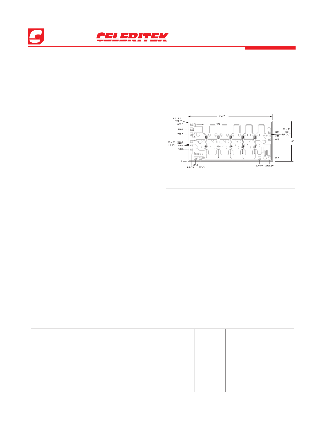
Chip Diagram
Specifications (TA= 25°C, V
DD
= 5V)
(On-Wafer Probe)
Parameters Units Min Typ Max
Frequency Range — 30 kHz 32.0 GHz
Small Signal Gain dB 11.0 12.0
Gain Flatness ±dB 0.5
Input VSWR — 1.8:1
Output VSWR — 1.7:1
Power Output (@1 dB Gain Compression) @ 9 GHz dBm +18.0
Current mA 100 150
Units in Microns
3236 Scott Boulevard, Santa Clara, California 95054
Phone: (408) 986-5060 Fax: (408) 986-5095
CMM2032-BD
Advanced Product Information - February 2003
(2 of 4)
Absolute Maximum Ratings
Parameter Rating
Drain Voltage 12 V
Gate Voltage -5 V
Drain Current 375 mA
Continuous Power Dissipation 3.0 W
Channel Temperature +175°C
Storage Temperature -65°C to +175°C
Mounting Temperature +320°C
Input Power +23 dBm
Die Attach and Bonding Procedures
Die Attach: Eutectic die attach is recommended. For eutectic die attach: Preform: AuSn (80% Au, 20% Sn); Stage
Temperature: 290°C, ±5°C; Handling Tool: Tweezers; Time: 1
min or less.
Wire Bonding: Wire Size: 0.7 to 1.0 mil in diameter (prestressed); Thermocompression bonding is preferred over
thermosonic bonding. For thermocompression bonding:
Stage Temperature: 250°C; Bond Tip Temperature: 150°C;
Bonding Tip Pressure: 18 to 40 gms depending on size of
wire.
Performance Optimization
Using the Gain-Ctl facility of the CMM2032-BD, output power may be increased by application of 1.2 to 1.8 Volts
to the Bias Control pad. If the Gain-Ctl facility is not used, a
fixed voltage at the Bias Control pad can be implemented by
connecting a off-chip parallel resistor to the pad which will
lower the output voltage accordingly.
If Bias Control voltage is decreased further than those
lowest values given in the tables, both gain and output power
will start to drop.
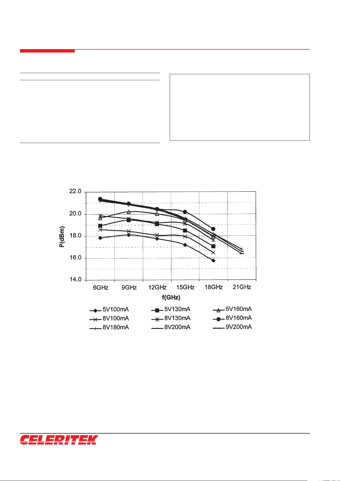
Typical Performance
P1dB vs Frequency
 Loading...