

CELER CMM1530-LC Datasheet
3236 Scott Boulevard Santa Clara, California 95054 Phone: (408) 986-5060 Fax: (408) 986-5095
CMM1530-LC
Features
❏ Operation as Low as 3.0V
❏ 38% Linear Power Added Efficiency
❏ +30 dBm Output Power (IS-136 TDMA Mode)
❏ +28.5 dBm Output Power (IS-98 CDMA Mode)
❏ 32 dB Gain at Operating Output
❏ Tested Under Digital Modulation
❏ New Low-Cost, Thermally Enhanced,
LCC-8 Package
❏ PHEMT Material Technology
Applications
❏ PCS Handsets
❏ PCS Base Stations
❏ Wireless Local Loop Subscriber Units
❏ CDMAone Handsets
Description
The CMM1530-LC is a linear power amplifier
intended for use in PCS handsets and wireless local loop subscriber units. The amplifier can be biased to meet the requirements of PCS-1900, IS-136 (TDMA), IS-98 (CDMA) or DCS1800 systems. It is a member of Celeritek’s new Triniti DX
Pro™ family of 3V power amplifier MMICs.
The CMM1530-LC is packaged in a low-cost, space
efficient, LCC-8 package that provides excellent electrical stability and low thermal resistance. The part requires minimal
external circuitry for bias and matching to reduce space and
cost.
This device is unconditionally stable under all source
and load impedances.
1.85 to 1.91 GHz
3.0V, 30 dBm, PCS/PCN
LCC-8 Power Amplifier
Advanced Product Information
November 2002
(1 of 4)
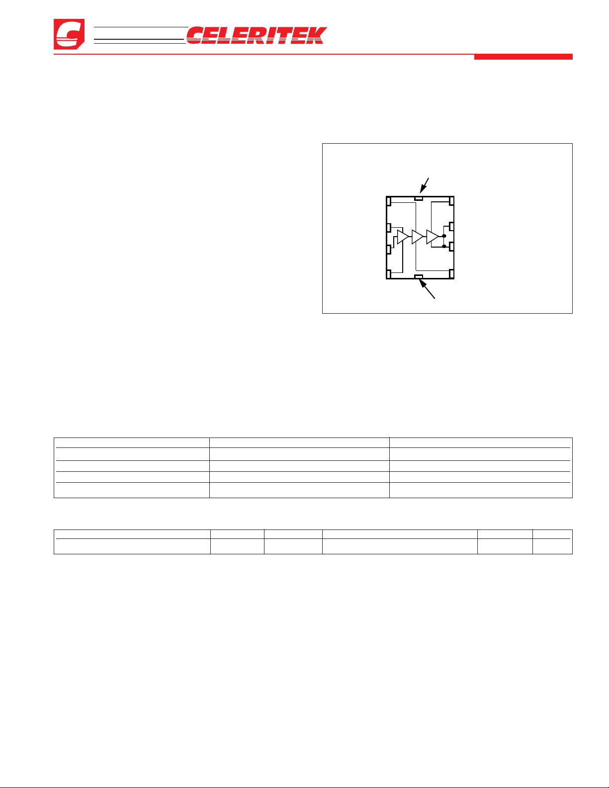
Ground Tab
Vg2 1
Vd1 4
Vg1 2
RF IN 3
7 RF OUT/V
d3
8 V
g3
5 V
d2
6 RF OUT/V
d3
Ground Tab
Functional Block Diagram
Absolute Maximum Ratings
Parameter Rating Parameter Rating Parameter Rating
Drain Voltage (+Vd) +5.5 V* Power Dissipation 5 W Operating Temperature -40°C to +90°C
Drain Current (Id) 1.8 A Thermal Resistance 20°C/W Channel Temperature 150°C
RF Input Power 3 dBm* Storage Temperature -65°C to +150°C Soldering Temperature 260°C for 5 Sec.
DC Gate Voltage (-Vg) -3.0 V*
Recommended Operating Conditions
Parameter Typ Units Parameter Typ Units
Drain Voltage (+Vd) 3.0 to 4.2 Volts Operating Temperature (PC Board) -30 to +80 °C
* Max (+Vd) and (-Vg) under linear operation. Max potential difference across the device at 1dB gain compression point (2V
d
+ |-Vg|) not to exceed the minimum breakdown voltage (Vbr) of +12V.
Application Information
The CMM1530-LC is a three stage amplifier that requires
a positive and a negative supply voltages for proper operation.
It is essential when turning on the device that the negative supply be applied before the positive supply. When turning the
device off, the positive supply should be removed before the
negative supply is removed.
The CMM1530-LC can be operated over a range of supply voltages and bias points. It is important that the maximum
power dissipation of the package be observed at all times and
that the maximum voltage across the device is not exceeded.
Circuit Design Considerations
Biasing Negative gate voltages are necessary to set the bias
currents of the three FET stages in the CMM1530-LC. The
first stage gate bias voltage is applied to Vg1 (Pin 2). The second stage gate bias voltage is applied to Vg2 (Pin 1), while the
third stage FET gate bias is applied to Vg3 (Pin 8). It is desirable to use one or more DACs (digital to analog converters)
along with appropriate divider networks, in order to adjust the
quiescent currents to within 10 mA of the target values. As an
example, for CDMA applications the target quiescent current
of the third FET is 85 mA, while those for the second and the
first FETs are 45 and 15 mA, respectively. The total quiescent
is 135 mA. It is also recommended that the quiescent currents
be set in the following sequence: the third stage FET is set
first, followed by the second stage FET, followed by the first
stage FET. The negative supply voltages control the quiescent
currents through each of the FETs and, therefore, control the
output power, adjacent channel power ratios, and the currents
at the full output power.
The positive supply voltages are applied to Pins 4, 5, 6
and 7.
– Continued on Page 2 –
3236 Scott Boulevard, Santa Clara, California 95054
Phone: (408) 986-5060 Fax: (408) 986-5095
CMM1530-LC
Advanced Product Information - November 2002
(2 of 4)
Parameter Condition Min Typ Max Units
Frequency Range 1.85 1.91 GHz
Gain @ Digital power output 28 31 dB
Gain Ripple* 1805-1880 MHz & 1850-1910 MHz 1.5 dB
Gain Variation Over supply voltage 2 dB/V
Over temperature 0.03 dB/°C
Power Output Control Range Vdd = 0 V to +3.5 V 50 dB
Power Output Meets IS-136 TDMA mask +30.0 dBm
Meets IS-98 CDMA mask +28.5 dBm
Harmonics 2nd @ Digital power output, no output trapping, Po=+28.5 dBm -30 dBc
3rd @ Digital power output, no output trapping, Po=+28.5 dBm -40 dBc
Noise Power in Receive Band 30 kHz bandwidth -94 dBm
Linearity CDMA modulation @ +28.5 dBm Pout, 1.25 MHz offset -45 dBc/30KHz
TDMA modulation @ +30 dBm Pout - Adjacent -26 dBc
TDMA modulation @ +30 dBm Pout - Alternate -45 dBc
Spurious Signal VSWR = 3:1 in-band, VSWR = 10:1 out-of-band -80 dBc
Noise Figure 3.0 dB
Input Return Loss 10 dB
Output Return Loss 8dB
Efficiency (Vdd = 3.0 V) Pout = +30.0 dBm - TDMA 36 38 %
Pout = +28.5 dBm - CDMA 32 35 %
Positive Supply Current (Id) Pout IS-136 TDMA 750 mA
Pout IS-98 CDMA 595 mA
Quiescent Current (Iq) No RF CDMA mode 130 mA
No RF TDMA mode 200 mA
Negative Supply Current (-Ig) Includes external resistor divider 1.1 2.0 mA
Negative Supply Voltage (-Vg) Into external resistor divider -0.5 -0.8 -1.4 V
Electrical Characteristics
Unless otherwise specified, the following specifications are guaranteed at room temperature with drain voltage (+Vd) = 3.5 V in Celeritek test fixture.
* Specifications guaranteed over the temperature range of -20°C to +80°C
It is very important to provide adequate de-coupling
between the RF and DC signals in designing the DC bias circuit. Inadequate by-pass capacitance and inductance around the
DC supply lines can compromise the adjacent channel power
ratio (ACPR), or reduce power gain and/or create oscillations.
The recommend DC by-pass capacitance and low-pass in-line
inductance are shown in the evaluation board on Page 4.
Matching Circuits Output matching and input matching circuits are required to achieve the RF specifications in this data
sheet. The recommend matching circuits are identical to the
matching circuits for the evaluation board shown on Page 4.
For output power matching, one shunt capacitor along the
transmission line connected to Pins 6 and 7 as well as the bond
wire inside the package from the output leads to the output
FET are used to transform 50Ω impedance to the load line
resistance of the output FET. The placement and the value of
the capacitor are important in achieving the performance
desired. Matching circuits for the frequencies other than the
one shown can be achieved by changing the capacitor value
and the placement position of the capacitor. The device can be
designed to work from UHF to around 3 GHz.
Supply Ramping To obtain power ramping, gate supply control is recommend. Drain supply voltage ramping can also be
used.
Modulation When biased as specified, the CMM1530-LC
will achieve the required adjacent channel response for the
digital PCS system specified. Celeritek tests each product
under digital modulation to ensure correlation to customer
applications.
Thermal
1. The copper pad on the backside of the CMM1530-LC must
be soldered to the ground plane.
2. All 8 leads of the package must be soldered to the appropriate electrical connection.
– Continued from Page 1 –
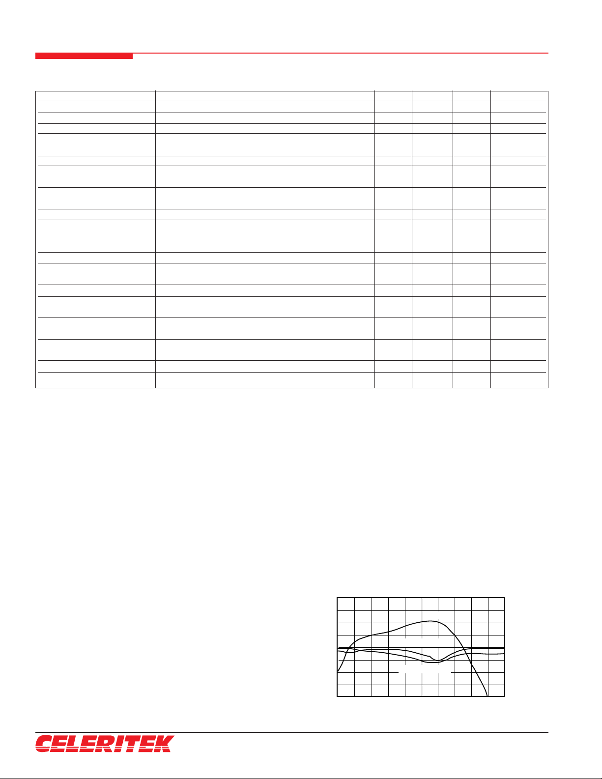
Wideband Gain & Return Loss
vs Frequency @ 3.5 V, +25°C
353025
20
Gain, dB
0.5
1.5
2.0
2.5
3.0
Frequency, GHz
-40
-30
-20
-10
0
Return Loss, dB
Gain
Input Return Loss
Output Return Loss
1.0
Typical Performance
 Loading...