

CELER CMM1331-SM Datasheet
3236 Scott Boulevard Santa Clara, California 95054 Phone: (408) 986-5060 Fax: (408) 986-5095
CMM1331-SM
Features
❏ 32.0 dBm (Typ.) Saturated Output Power
❏ 32.0 dB (Typ.) Linear Gain
❏ Fully Matched
❏ Unconditionally Stable
❏ Low-Cost Surface Mount Package
❏ Optimum Thermal Dissipation
Applications
❏ Ku-Band VSAT Transmit Subsystems
Description
The CMM1331-SM is a four-stage pHEMT GaAs
MMIC power amplifier that is ideally suited for transmit
subsystems designed for Ku-Band VSAT applications. The
CMM1331-SM provides 32.0 dB linear gain and delivers
1.5 watts of output power at saturation operating from
12.70 to 13.50 GHz frequency.
The unconditional stability and internal matching
provides for reduction of external components making this
product a simple and low-cost solution. The low-cost, 6mm x
6mm x 1.6mm surface mount package offers the same excellent RF and thermal properties as a typical flange package.
12.70 to 13.50 GHz
1.5 Watt Power Amplifier
Advanced Product Specifications
October 2003
(1 of 2)
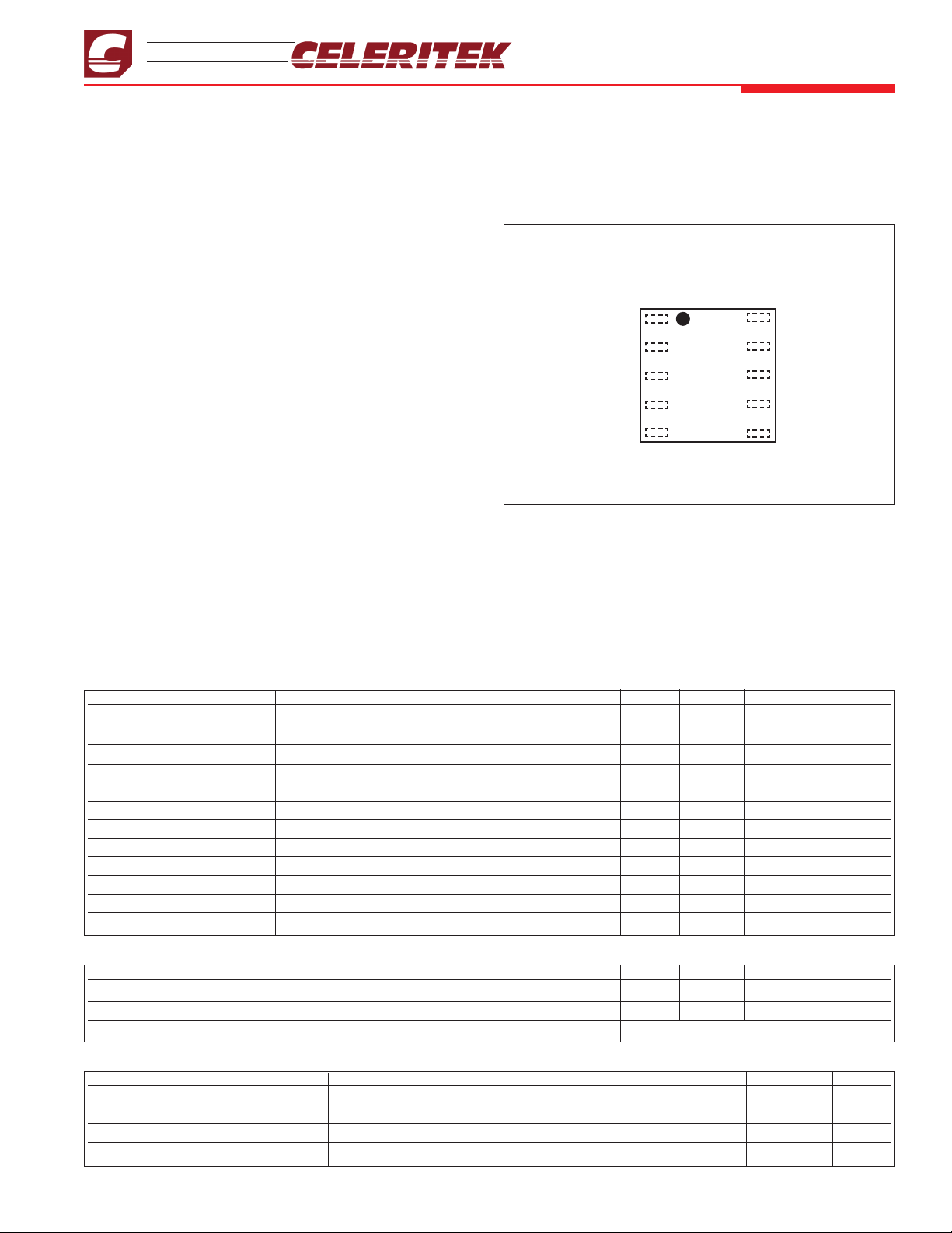
Pin Functional Diagram
Parameter Condition Min Typ Max Units
Frequency Range 12.70 13.50 GHz
Output Power @ 1dB compression 30.0 31.0 dBm
Saturated Output Power Pout at Pin = 5.0 dBm 31.0 32.0 dBm
Output Power Variation Over operating frequency 1.0 1.5 dBm
Linear Gain 29.0 32.0 35.0 dB
Linear Gain Variation Over operating frequency 2.0 dB
Third Order Intercept Point 36.0 dBm
Input Reflection Coefficient -10.0 dB
Output Reflection Coefficient -7.0 dB
Gate Supply Voltage Idq = 770 mA -1.1 -0.9 -0.7 Volt
Drain Current At Saturation 900 980 mA
Power Added Efficiency At Saturation 22 26 %
Electrical Characteristics
(T = +25°C, Vdd = 7V, Idq = 770mA)
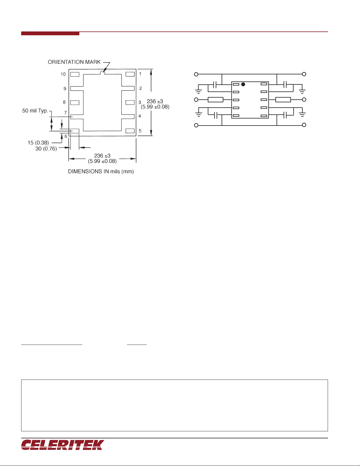
Vdd 1
GROUND 2
RF IN 3
GROUND 4
Vgg 5
10 Vdd
9 GROUND
8 RF OUT
7 GROUND
6 Vgg
CMM1331-SM
Maximum Ratings
(TA = -40°C to +75°C) Operation outside these limits can cause permanent damage.
Parameter Typ Units Parameter Typ Units
Drain Voltage (+Vdd) 8.5 Volts RF Input Power (Pin) 7.0 dBm
Gate Voltage (Vgg) -3.0 Volts Dissipated Power (P
diss
) 7.2 Watts
Quiescent Current (Idq) 1000 mA Storage Temperature -50 to +150 °C
Gate Current (Ig) 5 mA Operating Backside Temperature -40 to +75 °C
Parameter Condition Min Typ Max Units
Saturated Output Power Variation from Room Temperature -0.5 dBm
Linear Gain Variation from Room Temperature -2.5 3.5 dB
Stability Unconditionally stable
Electrical Specifications
(TA = -40°C to +75°C)
3236 Scott Boulevard, Santa Clara, California 95054
Phone: (408) 986-5060 Fax: (408) 986-5095
CMM1331-SM
Advanced Product Specifications - October 2003
(2 of 2)
Celeritek reserves the right to make changes without further notice to any products herein. Celeritek makes no warranty, representation or guarantee regarding the
suitability of its products for any particular purpose, nor does Celeritek assume any liability arising out of the application or use of any product or circuit, and specifically
disclaims any and all liability, including without limitation consequential or incidental damages. “Typical” parameters can and do vary in different applications. All operating
parameters, including “Typicals” must be validated for each customer application by customer’s technical experts. Celeritek does not convey any license under its patent
rights nor the rights of others. Celeritek products are not designed, intended, or authorized for use as components in systems intended for surgical implant into the body,
or other applications intended to support or sustain life, or for any other application in which the failure of the Celeritek product could create a situation where personal
injury or death may occur. Should Buyer purchase or use Celeritek products for any such unintended or unauthorized application, Buyer shall indemnify and hold Celeritek
and its officers, employees, subsidiaries, affiliates, and distributors harmless against all claims, costs, damages, and expenses, and reasonable attorney fees arising out
of, directly or indirectly, any claim of personal injury or death associated with such unintended or unauthorized use, even if such claim alleges that Celeritek was negligent
regarding the design or manufacture of the part. Celeritek is a registered trademark of Celeritek, Inc. Celeritek, Inc. is an Equal Opportunity/Affirmative Action Employer.
Ordering Information
The CMM1331-SM is available in available in tube or tape and reel.
Part Number for Ordering
Package
CMM1331-SM Surface mount package
Physical Dimensions (Bottom View)
Vgg
RF IN
CMM1331-SM
1
2
3
4
5
10
9
8
7
6
Vdd
RF OUT
0.1 µF
0.1 µF
0.1 µF 0.1 µF
Vgg
Vdd
50 Ω
50 Ω
Recommended Application Circuit
Note: This schematic represents the topology of the application circuit
recommended by Celeritek.
Note: Due to the high gain of this device it is highly recommended to maintain the
reverse isolation (S12) above 50 dB.
Biasing Notes
1. Dual bias is required
2. 0.1µF bypass capacitors are needed on PC board as close as possible to pins
1, 5, 6 and 10.
3. Positive (+) bias can be applied either at pin 1 or pin 6.
4. Negative (-) bias can be applied either at pin 5 or pin 6.
5. No DC block is required at RF IN/OUT.
6. Negative (-) bias must be applied before applying positive (+) bias.
 Loading...