

CELER CMM0530-LC-00TT, CMM0530-LC-00T0, CMM0530-LC-00ST, CMM0530-LC-00S0 Datasheet
3236 Scott Boulevard Santa Clara, California 95054 Phone: (408) 986-5060 Fax: (408) 986-5095
CMM0530-LC
Features
❏ Multi-Mode Operation as Low as 3.0V
❏ 42% Linear PowerAdded Efficiency
❏ 55% Analog PowerAdded Efficiency
❏ New Low-Cost, Plastic LCC-8 Package
❏ 29 dB Gain
❏ Tested Under Digital Modulation
❏ PHEMT Material Technology
Applications
❏ IS-98/AMPS Handsets
❏ IS-136/AMPS Cellular Handsets
❏ 900 MHz ISM Band Products
❏ Wireless Local Loop SubscriberTerminals
Description
The CMM0530-LC is a highly efficient multi-mode
power amplifier GaAs MMIC intended for use in portable telephone handsets and data communications products for wireless
communications. It meets the handset requirements for cellular
AMPS, and the CDMA and TDMA digital standards for the US
cellular wireless communications. CMM0530-LC is a member
of the new
Triniti DX Pro
™ amplifier family whose members
are pin-compatible and all operate under 3.5V bias voltage. The
CMM0530-LC is packaged in a low-cost, plastic, LCC-8 power
package. It has low thermal impedance and low RF loss. The
device requires minimum amount of external biasing and RF
matching circuits.
824 to 928 MHz
3.0V, 30.5 dBm Multi-Mode
Plastic LCC-8 PowerAmplifier
Advanced Product Information
May 1999
(1 of 4)
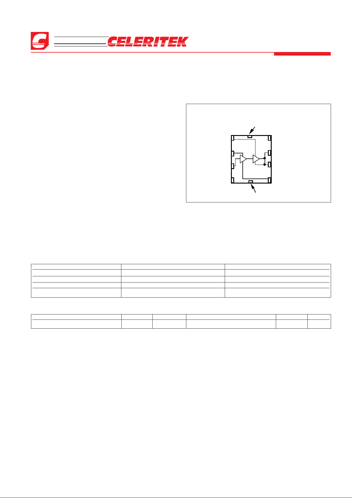
Ground Tab
Vg2 1
N/C 4
Vg1 2
RF IN 3
7 RF OUT/V
d2
8 N/C
5 Vd16 RF OUT/V
d2
Ground Tab
Functional Block Diagram
Recommended Operating Conditions
Parameter Typ Units Parameter Typ Units
Drain Voltage (+Vd) 3.0 to 4.2 Volts Operating Temperature (PC Board) -30 to +80 °C
Absolute Maximum Ratings
Parameter Rating Parameter Rating Parameter Rating
Drain Voltage (+Vd) +5.5 V* Power Dissipation 5 W Operating Temperature -40°C to +90°C
Drain Current (Id) 1.8 A Thermal Resistance 20°C/W Channel Temperature 150°C
RF Input Power +10 dBm* Storage Temperature -65°C to +150°C Soldering Temperature 260°C for 5 Sec.
DC Gate Voltage (-Vg) -3.0 V*
* Max (+Vd) and (-Vg) under linear operation. Max potential difference across the device at 1 dB gain compression point (2Vd+ |-Vg|) not to exceed the minimum breakdown voltage (Vbr) of +12V.
Application Information
The CMM0530-LC is a two-stage amplifier that requires
both positive and negative power supplies for proper operation.
It is essential that the negative supply be applied first during
turn-on and last during turn-off. Otherwise, the device may be
damaged.
The CMM0530-LC can be operated over a wide range of
positive and negative voltages to obtain various power, linearity
and efficiency performance. However, it is important to keep
the maximum DC power and the bias voltages within the specified absolute maximum rating to prevent over stressing the
device either electrically or thermally.
Design Considerations
Biasing Negative gate voltages are necessary to set the bias
currents of the two FET stages in the CMM0530-LC. The first
stage gate bias voltage is applied to Vg1 (Pin 2). The second
stage gate bias voltage is applied to Vg2 (Pin 1). It is desirable
to use one or more DACs (digital to analog converters) along
with appropriate resistor divider networks, when necessary, in
order to adjust the quiescent currents to within 10 mA of the
targeted values. As an example, for CDMA applications the target quiescent current of the second FET is 120 mA, while that
of the first is 50 mA. The total quiescent is 170 mA. It is also
recommend that the quiescent currents be set in the following
sequence: the second stage FET is set first, followed by the first
stage FET. The negative supply voltages control the quiescent
currents through each FET and, therefore, control the output
power, adjacent channel power ratio, and the currents at full
output power.
The positive supply voltages are applied to Pins 5, 6 and 7.
It is very important to provide adequate de-coupling
between the RF and the DC signals in designing the DC bias
circuit. Inadequate by-pass capacitance around the DC supply
lines and inductance can compromise the adjacent channel
power ratio (ACPR), or reduce power gain and/or create oscillations. The recommend DC by-pass capacitance and low-pass
– Continued on Page 2 –
3236 Scott Boulevard, Santa Clara, California 95054
Phone: (408) 986-5060 Fax: (408) 986-5095
Digital Bias Analog Bias
Parameter Condition Min Typ Max Min Typ Max Units
Frequency Range 824 928 824 928 MHz
Pout - TDMA Operation Meets IS-136 TDMA mask +30.0 dBm
Pout - CDMA Operation Meets IS-98 CDMAmask +28.5 dBm
Pout - Analog Operation AMPS (under dual mode operation) +31.5 dBm
Efficiency IS-136 TDMA @ +30 dBm 42 %
IS-95 CDMA @ +28 dBm 37 %
AMPS @ +31.5 dBm
(under dual mode operation) 55 57 %
Harmonics 2nd @ Pout = +31.5 dBm -30 dBc
3rd @ Pout = +31.5 dBm -35 dBc
Adjacent Channel Power Pout = +30 dBm TDMA ±30 KHz -26 dBc
Alternate Channel Power Pout = +30 dBm TDMA ±60 KHz -45 dBc
Adjacent Channel Power Pout = +28 dBm CDMA ±898 KHz -45 dBc/30 KHz
Alternate Channel Power Pout = +28 dBm CDMA ±1980 KHz -55 dBc/30 KHz
Noise Power in Receive Band 30 kHz BW -94 dBm
Gain @ Pout = +28.5 dBm, +30 dBm 26 29 dB
@ Pout = +31.5 dBm 24 27 dB
Gain Ripple 824-849 or 880-910 MHz 1.5 1.5 dB
Gain Variation Over supply voltage 2 2 dB/V
Gain Variation Over temperature 0.03 0.03 dB/°C
Power Output Control Range Vdd = 0 to 3.5 V 50 dB
Quiescent Current No RF, TDMA mode 200 mA
No RF, CDMA mode 170 mA
Noise Figure 3.5 3.5 dB
VSWR Input (In Celeritek test fixture) 2.0:1 2.0:1
Stability 8:1 VSWR in band -80 -80 dBc/30 KHz
10:1 VSWR out of band -80 -80 dBc/30 KHz
Electrical Characteristics
Unless otherwise specified, the following specifications are guaranteed at room temperature with drain voltage (+Vd) = 3.5 V, in Celeritek test fixture.
CMM0530-LC
Advanced Product Information - May 1999
(2 of 4)
in-line inductance are shown in the evaluation board on page 4.
Matching Circuits Output matching and input matching cir-
cuits are required to achieve the RF specifications in this data
sheet. The recommend matching circuits are identical to the
matching circuits for the evaluation board shown on Page 4.
For output power matching, shunt capacitors along the transmission line connected to Pins 6 and 7 as well as the bond
wire inside the package from the output leads to the output
FET are used to transform 50Ω impedance to the load line
resistance of the output FET. The placements and the values
of the capacitor are important in achieving the performance
desired. Matching circuits for frequencies other than the one
shown can be achieved by changing the capacitor value and
the placement position of the capacitor. The device can be
designed to work from UHF to around 3 GHz.
Supply Ramping To obtain power ramping, gate supply control is recommended. Drain supply voltage can also be used.
Modulation When biased as specified, the CMM0530-LC will
achieve the required adjacent channel response for the digital
system specified. Celeritek tests each product under digital
modulation to ensure correlation to customer applications.
Thermal
1. The copper pad on the backside of the CMM0530-LC must
be soldered to the ground plane.
2. All 8 leads of the package must be soldered to the appropriate electrical connection.
– Continued from Page 1 –
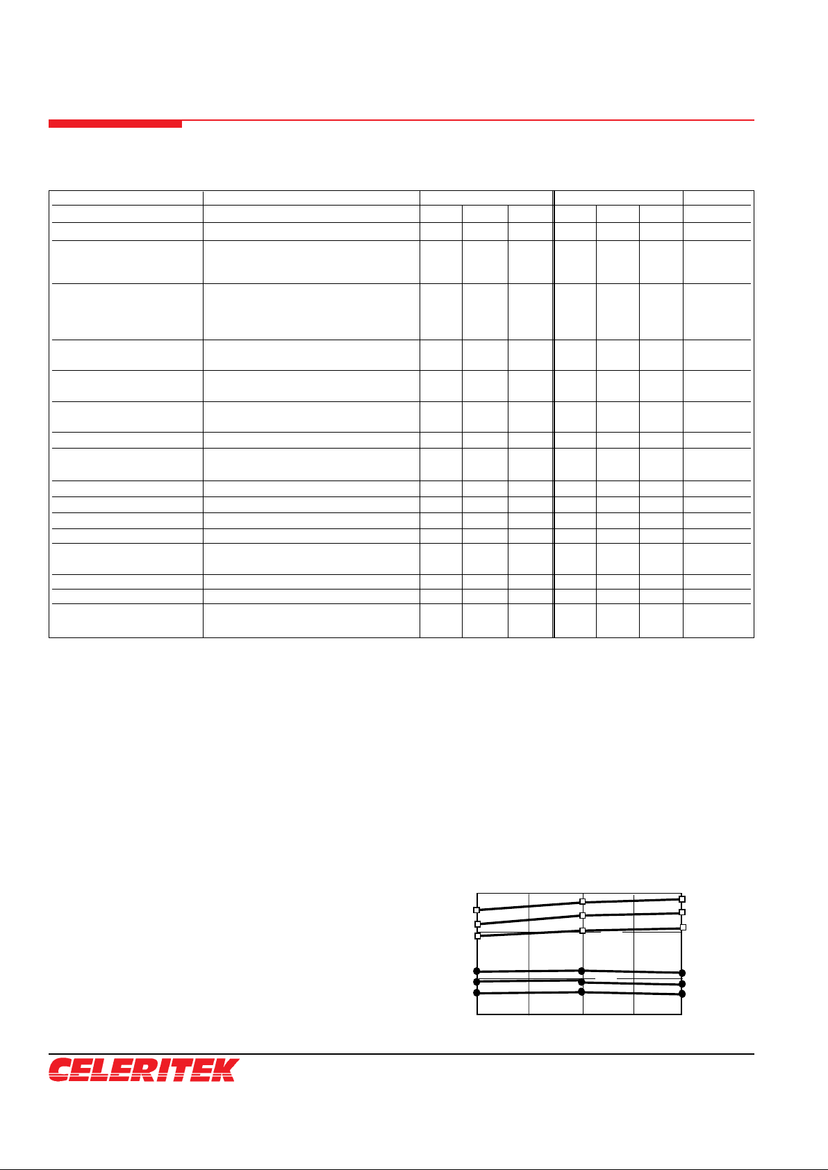
Typical Performance
Gain & IS-136 TDMA Output Power
vs Frequency Over Voltage @ +25°C
Frequency, MHz
824
849
27.5
29.5
29.5
31.5
Gain, dB
3.0 V
3.3 V
2.7 V
Power Out, dBm
3.0 V
3.3 V
2.7 V
 Loading...