

CELER CMM0333-AK-000T, CMM0333-AK Datasheet
3236 Scott Boulevard Santa Clara, California 95054 Phone: (408) 986-5060 Fax: (408) 986-5095
CMM0333
Features
❏ Multi-Mode Operation from 5V Supply
❏ 40% Linear Power Added Efficiency
❏ 32.5 dBm with 55% Power Added Efficiency
❏ 32 dBm Output Power (IS-136 TDMA)
❏ 42 dB Gain
❏ Tested Under Actual Digital Modulation
❏ Low Cost, SO-8 Surface Mount Package
Applications
❏ IS-136/AMPS Cellular Handsets
❏ 900 MHz ISM Band Products
❏ Wireless Local Loop SubscriberTerminals
Description
The CMM0333 is a highly efficient 5V, multi-mode
power amplifier intended for use in portable cellular handsets
and datacom products operating in the AMPS and 902-928 MHz
bands. As a pin-compatible member of the new
Triniti DX
™
amplifier family, the CMM0333 offers maximum performance
and flexibility. The CMM0333 is packaged in a low-cost,
space efficient SO-8 power package that gives excellent electrical stability and thermal handling performance with a R
Θ
of less than 18° C/W. The part is designed to require minimal
external circuitry for bias matching, simplifying design and
keeping board space and cost to a minimum.
824 to 849 MHz
5V, 32 dBm Multi-Mode
Power Amplifier
Preliminary Product Information
September 1996
(1 of 2)
Back plane is ground and
must be soldered to thermally
conductive ground plane.
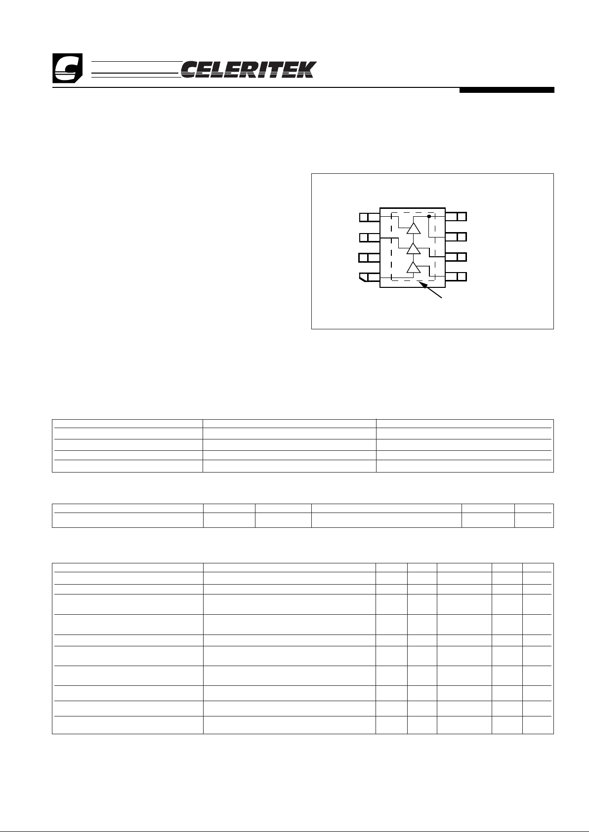
Vg2 4
RF IN 1
Vg1 3
GND 2
6 RF OUT/V
d3
5 RF OUT/V
d3
8 Vd17 V
d2
Functional Block Diagram
Absolute Maximum Ratings
Parameter Rating Parameter Rating Parameter Rating
Drain Voltage (+Vd) +9.0 V* Power Dissipation 5 W Operating Temperature -40°C to +85°C
Drain Current (Id) 1.8 A Thermal Resistance 18°C/W Channel Temperature 175°C
RF Input Power +15 dBm Storage Temperature -65°C to +150°C Soldering Temperature 260°C for 5 Sec.
DC Gate Voltage (Vg) -2.5 V
Recommended Operating Conditions
Parameter Typ Units Parameter Typ Units
Drain Voltage (+Vd) 4.5 to 5.1 Volts Operating Temperature (PC Board) -30 to +80 °C
* 9.0V max (+Vd) under linear operation. Max potential difference across the device (2Vd+ |Vg|) not to exceed the minimum breakdown voltage (Vbr) of 18V in RF compression.
Parameter Condition Min Typ Std Deviation Max Units
Frequency Range 824 849 MHz
Gain @ Digital power output 39 42 1.5 dB
Power Output Meets IS-136 TDMA mask 31 32 0.7 dBm
With Pin = 0 dBm AMPS mode 32.0 32.5 dBm
Harmonics 2nd @ Pout = +32 dBm -30 dBc
3rd @ Pout = +32 dBm -35 dBc
Return Loss 10 dB
Efficiency 32 dBm Pout IS-136 TDMA 35 40 2 %
32.5 dBm Pout / Pin = 0 dBm AMPS mode 50 55 %
Positive Supply Current (Id) 32 dBm Pout IS-54, IS-136 TDMA 675 mA
32.5 dBm Pout / Pin = 0 dBm AMPS mode 700 mA
Quiescent Current (Iq) No RF 350 mA
Negative Supply Current (-Ig) Includes external resistor divider 1.1 0.2 2.0 mA
Negative Supply Voltage (-Vg) Into external resistor divider -1.3 -1.7 0.16 -2.2 V
Electrical Characteristics
Unless otherwise specified, the following specifications are guaranteed at room temperature with drain voltage (+Vd) = 4.8 V in Celeritek test fixture
3236 Scott Boulevard, Santa Clara, California 95054
Phone: (408) 986-5060 Fax: (408) 986-5095
Celeritek reserves the right to make changes without further notice to any products herein. Celeritek makes no warranty, representation or guarantee regarding the
suitability of its products for any particular purpose, nor does Celeritek assume any liability arising out of the application or use of any product or circuit, and specifically
disclaims any and all liability, including without limitation consequential or incidental damages. “Typical” parameters can and do vary in different applications. All operating
parameters, including “Typicals” must be validated for each customer application by customer’s technical experts. Celeritek does not convey any license under its patent
rights nor the rights of others. Celeritek products are not designed, intended, or authorized for use as components in systems intended for surgical implant into the body, or
other applications intended to support or sustain life, or for any other application in which the failure of the Celeritek product could create a situation where personal injury
or death may occur. Should Buyer purchase or use Celeritek products for any such unintended or unauthorized application, Buyer shall indemnify and hold Celeritek and
its officers, employees, subsidiaries, affiliates, and distributors harmless against all claims, costs, damages, and expenses, and reasonable attorney fees arising out of,
directly or indirectly, any claim of personal injury or death associated with such unintended or unauthorized use, even if such claim alleges that Celeritek was negligent
regarding the design or manufacture of the part. Celeritek is a registered trademark of Celeritek, Inc. Celeritek, Inc. is an Equal Opportunity/Affirmative Action Employer.
Ordering Information
The CMM0333 is available in a surface mount SO-8 power package and devices are available in tape and reel.
Part Number for Ordering Package
CMM0333-AK SO-8 surface mount power package
CMM0333-AK-000T SO-8 surface mount power package in tape and reel
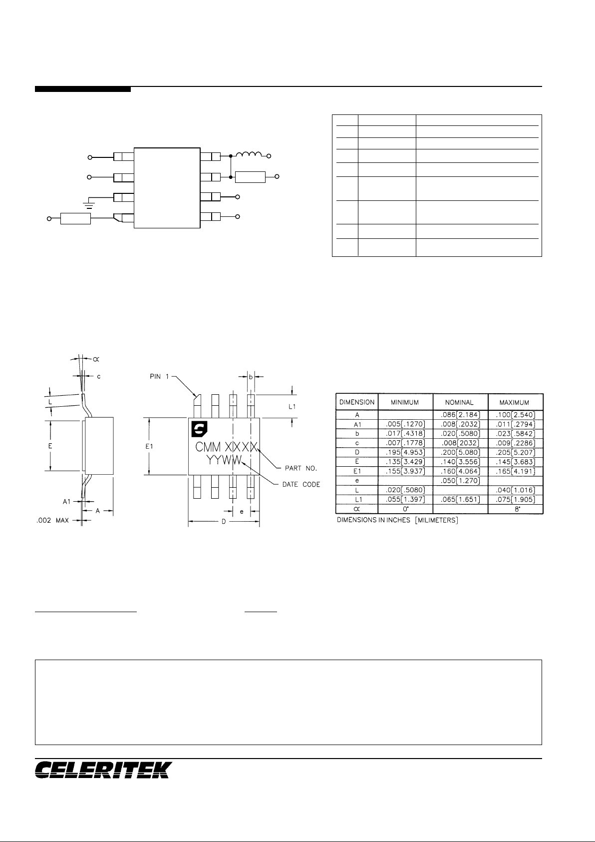
Physical Dimensions
CMM0333
Advanced Product Information - September 1996
(2 of 2)
Pin # Name Description
1 RF IN RF input
2 GND Ground
3 V
g1
Input stage gate bias
4 V
g2
Output stage gate bias
5 RF OUT/V
d3
RF output and Vd3. External
matching circuit required
6 RF OUT/V
d3
RF output and Vd3. External
matching circuit required
7 V
d2
Second stage drain bias
8 V
d1
Input stage drain bias
RF INVg2
GNDVg1Vd243215678
MATCH
V
d3
MATCH
RF OUT/V
d3
V
d1
Connection Diagram and Pin Descriptions
 Loading...