

CELER CMM0224-BD Datasheet
3236 Scott Boulevard Santa Clara, California 95054 Phone: (408) 986-5060 Fax: (408) 986-5095
2.0 to 24.0 GHz
GaAs MMIC
Power Amplifier
Advanced Product Information
April 2003 (1 of 2)
Features
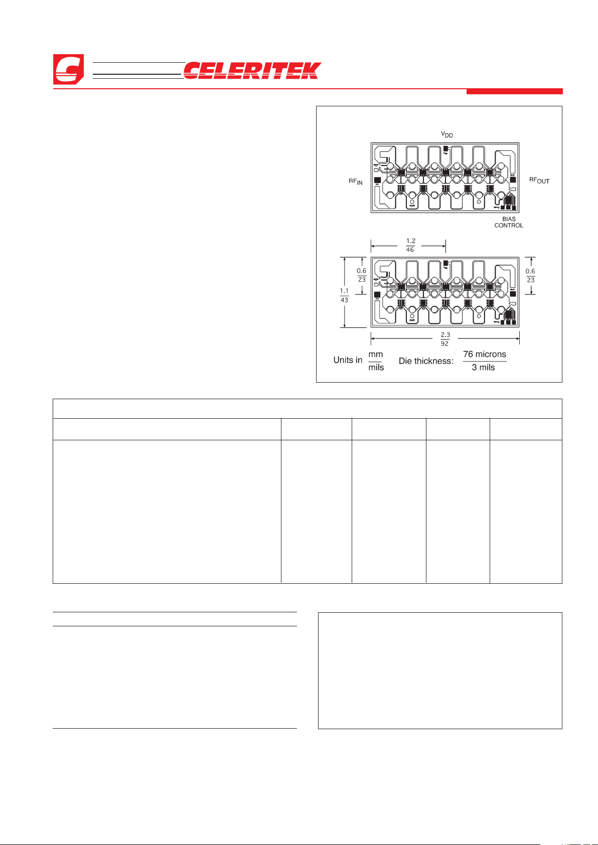
❏ Small Size: 43 x 92 mils
❏ High Gain
❏ Directly Cascadable
❏ Medium Power: +24 dBm
❏ Ion-Implanted Active Layers
❏ Silicon Nitride Passivation
Specifications (TA= 25°C, V
DD
= 8V)
Parameters Units Min Typ Max
Frequency Range GHz 2.0 24.0
Small Signal Gain dB 11.0 12.0
Gain Flatness ±dB 0.5 0.85
Input/Output VSWR — 1.8:1 2.0:1
Power Output (@1 dB Gain Compression) dBm 22.0 24.0
Second Order Intercept Point dBm 40.0
Third Order Intercept Point dBm 30.0
Current mA 300 330
Absolute Maximum Ratings
Parameter Rating
Drain Voltage 12V
Drain Current 360 mA
Continuous Power Dissipation 3.0 W
Channel Temperature +175°C
Storage Temperature -65°C to +175°C
Mounting Temperature +320°C
Input Power +23 dBm
Die Attach and Bonding Procedures
Die Attach: Eutectic die attach is recommended. For eutectic die attach: Preform: AuSn (80% Au, 20% Sn); Stage
Temperature: 290°C, ±5°C; Handling Tool: Tweezers; Time: 1
min or less.
Wire Bonding: Wire Size: 0.7 to 1.0 mil in diameter (prestressed); Thermocompression bonding is preferred over
thermosonic bonding. For thermocompression bonding:
Stage Temperature: 250°C; Bond Tip Temperature: 150°C;
Bonding Tip Pressure: 18 to 40 gms depending on size of
wire.
CMM0224-BD
Chip Diagram
3236 Scott Boulevard, Santa Clara, California 95054
Phone: (408) 986-5060 Fax: (408) 986-5095
CMM0224-BD
Advanced Product Information - April 2003
(2 of 2)
Celeritek reserves the right to make changes without further notice to any products herein. Celeritek makes no warranty, representation or guarantee regarding the
suitability of its products for any particular purpose, nor does Celeritek assume any liability arising out of the application or use of any product or circuit, and specifically
disclaims any and all liability, including without limitation consequential or incidental damages. “Typical” parameters can and do vary in different applications. All operating
parameters, including “Typicals” must be validated for each customer application by customer’s technical experts. Celeritek does not convey any license under its patent
rights nor the rights of others. Celeritek products are not designed, intended, or authorized for use as components in systems intended for surgical implant into the body, or
other applications intended to support or sustain life, or for any other application in which the failure of the Celeritek product could create a situation where personal injury
or death may occur. Should Buyer purchase or use Celeritek products for any such unintended or unauthorized application, Buyer shall indemnify and hold Celeritek and
its officers, employees, subsidiaries, affiliates, and distributors harmless against all claims, costs, damages, and expenses, and reasonable attorney fees arising out of,
directly or indirectly, any claim of personal injury or death associated with such unintended or unauthorized use, even if such claim alleges that Celeritek was negligent
regarding the design or manufacture of the part. Celeritek is a registered trademark of Celeritek, Inc. Celeritek, Inc. is an Equal Opportunity/Affirmative Action Employer.
Ordering Information
The CMM-0224-BD is available in bare die and is shipped in Gel Pak.
Part Number for Ordering
Package
CMM0224-BD Bare Die
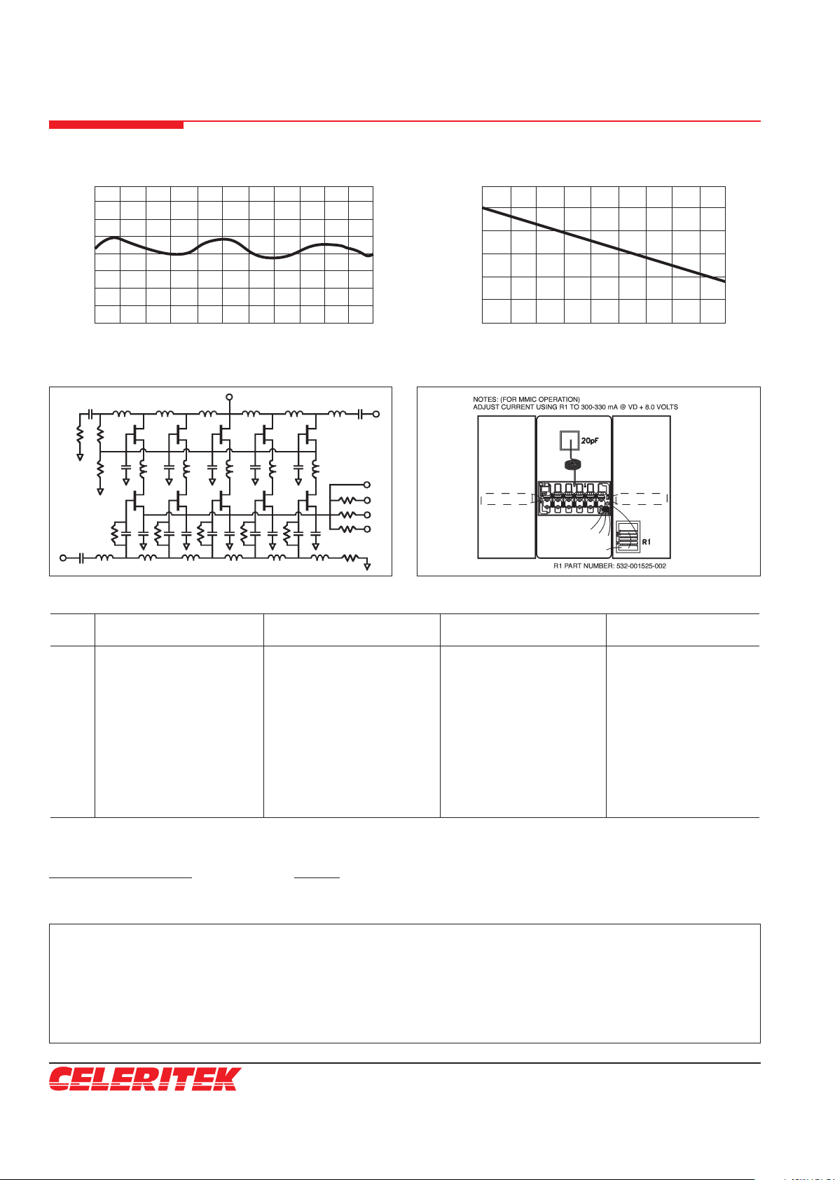
Optional Current Setting Resistor 532-001525-002
Typical Scattering Parameters, TA= 25°C (S-Parameters Include Bonding Wire Parasitics)
Freq S
11
S
21
S
12
S
22
(GHz) (dB) (Mag) (Ang) (dB) (Mag) (Ang) (dB) (Mag) (Ang) (dB) (Mag) (Ang)
2.0 -16.5 0.149623566 -121 12.2 4.073802778 139 -51.3 0.002722701 -6 -14.6 0.186208714 141
4.0 -16.4 0.151356125 -179 12.5 4.216965034 71 -42.6 0.007413102 1 -18.8 0.114815362 89
6.0 -19.7 0.103514217 108 12.2 4.073802778 9 -38.5 0.011885022 -59 -24.3 0.06095369 61
8.0 -25.8 0.051286138 -67 11.9 3.935500755 -50 -36.1 0.015667511 -114 -28.4 0.03801894 -112
10.0 -16.9 0.142889396 -152 12.2 4.073802778 -111 -33.0 0.022387211 -167 -21.5 0.084139514 -165
12.0 -15.8 0.16218101 151 12.2 4.073802778 -171 -32.3 0.024266101 145 -21.9 0.080352612 132
14.0 -22.6 0.074131024 106 11.9 3.935500755 129 -31.3 0.027227013 108 -21.9 0.080352612 -72
16.0 -19.7 0.103514217 -157 11.7 3.84591782 66 -32.3 0.024266101 49 -14.2 0.19498446 -130
18.0 -14.9 0.179887092 162 12.3 4.120975191 4 -32.1 0.024831331 -23 -12.1 0.248313311 -163
20.0 -19.2 0.10964782 162 12.2 4.073802778 -62 -30.0 0.031622777 -91 -11.2 0.27542287 -174
22.0 -15.1 0.175792361 175 12.0 3.981071706 -72 -28.8 0.036307805 -117 -10.6 0.295120923 179
24.0 -13.7 0.206538016 173 11.8 3.89045145 -71 -28.6 0.037153523 -126 -10.2 0.309029543 158
Schematic Diagram
Assembly Example
Typical Performance (TA=25°C, VDD = 8V)
27
26
25
24
23
22
21
2 4 6 8 10 12 14 16 18 20
FREQUENCY, GHz
OUTPUT POWER, +dBm
OUTPUT POWER VS FREQUENCY
2 4 6 8 10 12 14 16 18 20 22 42
FREQUENCY, GHz
14
13
12
11
10
GAIN, dB
GAIN VS FREQUENCY
 Loading...