

CELER CFK2162-P3-000T, CFK2162-P3 Datasheet
3236 Scott Boulevard Santa Clara, California 95054 Phone: (408) 986-5060 Fax: (408) 986-5095
CFK2162-P3
Features
❏ High Gain
❏ +34 dBm Power Output
❏ Proprietary Power FET Process
❏ >45% Linear Power Added Efficiency
❏ +29 dBm with 30 dBc Third Order Products
❏ Surface Mount SO-8 Power Package
Applications
❏ PCS/PCN Base Stations and Terminals
❏ Wireless Local Loop
Description
The CFK2162-P3 is a high-gain FET intended for driver amplifier applications in high-power systems, and output
stage usage in medium power applications at power levels up to
+34 dBm. The device is easily matched and provides excellent
linearity at 2 Watts. Manufactured in Celeritek’s proprietary
power FET process, this device is assembled in an industry
standard surface mount SO-8 power package that is compatible
with high volume, automated board assembly techniques.
1.8 to 2.0 GHz
+34 dBm Power GaAs FET
Product Specifications
July 1997
(1 of 4)
13478652GGD
D
Back Plane
is Source
GND
GND
GND
GND
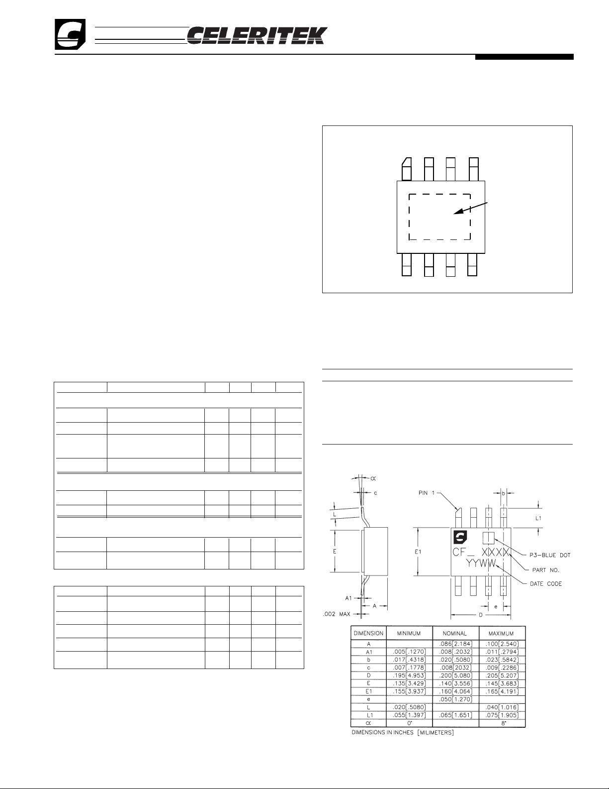
Package Diagram
Notes:
1. Sum to two tones with 1 MHz spacing = 29 dBm.
2. See thermal considerations information on page 4.
3.
Max (+Vd) and (-Vg) under linear operation. Max potential difference
across the device in RF compression (2Vd+ |-Vg|) not to exceed the minimum breakdown voltage (Vbr) of +18V.
Absolute Maximum Ratings
Parameter Symbol Rating
Drain-Source Voltage V
DS
12V
(3)
Gate-Source Voltage V
GS
-5V
Drain Current I
DS
Idss
Continuous Dissipation P
T
10W
Channel Temperature T
CH
175°C
Storage Temperature T
STG
-65°C to +175°C
Parameters Conditions Min Typ Max Units
Vd= 8V, Id= 800 mA (Quiescent)
P
-1dB
33.0 34.0 — dBm
SSG 13.0 14.0 — dB
3rd Order
Products
(1)
26 30 — dBc
Efficiency @ P1dB — 43 — %
Vd= 5V, Id= 350 mA (Quiescent)
P
-1dB
— 30.0 — dBm
SSG — 11.0 — dB
Vd= 5V, Id= 1200 mA (Quiescent)
P
-1dB
— 32.5 — dBm
SSG — 12.0 — dB
Specifications (TA= 25°C) The following specifications are
guaranteed at room temperature in Celeritek test fixture at 1.95 GHz.
Parameters Conditions Min Typ Max Units
g
m
Vds = 2.0V, Vgs = 0V — 1700 — mS
I
dss
Vds = 2.0V, Vgs = 0V — 2.8 — A
V
p
Vds = 3.0V, Ids = 65 mA — -1.8 Volts
BV
GD
(3) Igd = 6.5 mA 18 20 — Volts
ΘJL(2) @150°C TCH — 10 — °C/W
SO-8 Power Package Physical Dimensions
3236 Scott Boulevard, Santa Clara, California 95054
Phone: (408) 986-5060 Fax: (408) 986-5095
CFK2162-P3
Product Specifications - July 1997
(2 of 4)
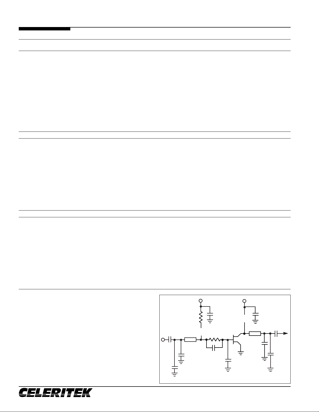
RF Match Data shown in the performance graphs was taken
in the test circuits shown at right and on page 3. Layout is
important for proper operation. Phase length of input and output 50Ω line varies as a function of exact desired frequency
of operation. Output shunt inductor effects output performance. Celeritek recommends the use of a high impedance
printed inductor Lambda/4 in length. Please contact the factory for an evaluation board and/or more detailed application
support.
Typical Scattering Parameters (TA= 25°C, Vds = 5 V, Ids = 350 mA)
Frequency S
11
S
21
S
12
S
22
(GHz) Mag Ang Mag Ang Mag Ang Mag Ang
0.6 0.946 -162.45 4.973 86.73 0.017 11.14 0.739 172.95
1.0 0.946 -176.06 2.885 73.75 0.018 9.37 0.748 169.73
1.1 0.946 -177.58 2.623 71.82 0.018 6.8 0.747 169.56
1.2 0.945 -178.58 2.424 69.66 0.019 6.59 0.746 169.16
1.3 0.944 -179.55 2.27 67.7 0.019 6.53 0.742 168.8
1.4 0.942 179.53 2.154 65.68 0.02 7.04 0.739 168.03
1.5 0.938 178.31 2.055 63.25 0.02 4.93 0.73 167.15
1.6 0.935 176.89 1.982 60.53 0.021 4.08 0.722 165.76
1.7 0.931 174.99 1.923 57.74 0.023 3.37 0.714 164.09
1.8 0.927 172.61 1.873 54.47 0.023 1.6 0.707 161.84
1.9 0.922 169.71 1.828 50.82 0.023 -0.79 0.70 158.98
2.0 0.918 166.09 1.777 46.63 0.025 -1.23 0.694 155.54
2.1 0.914 161.9 1.722 42.23 0.024 -4.64 0.69 151.93
2.2 0.912 157.79 1.664 37.59 0.026 -9.26 0.689 148.15
3.0 0.941 132.34 1.033 10.11 0.022 -27.73 0.76 128.69
3.5 0.957 134.66 0.803 6.12 0.02 -21.78 0.787 132.92
4.0 0.94 138.76 0.803 1.66 0.023 -20.57 0.74 136.51
(TA = 25°C, Vds = 5 V, Ids = 1200 mA)
0.6 0.95 -165 5.311 84.94 0.014 13.61 0.747 17.19
1.0 0.951 -177.94 3.044 72.23 0.014 14.39 0.749 168.92
1.3 0.951 178.92 2.391 66.48 0.015 13.62 0.741 167.98
1.4 0.949 177.92 2.272 64.41 0.015 14.21 0.734 167.24
1.5 0.946 176.83 2.169 61.99 0.016 14.13 0.728 166.28
1.6 0.943 175.5 2.09 59.58 0.017 12.30 0.72 165.01
1.7 0.939 173.67 2.029 56.57 0.017 12.06 0.712 163.24
1.8 0.935 171.39 1.98 53.44 0.018 10.27 0.703 161.07
1.9 0.931 168.6 1.93 49.72 0.019 5.75 0.696 158.27
2.0 0.929 165.15 1.88 45.76 0.02 7.43 0.69 154.9
2.1 0.925 161.29 1.822 41.44 0.02 4.37 0.686 151.32
2.2 0.924 157.02 1.757 36.86 0.021 2.36 0.687 147.44
3.0 0.947 131.72 1.09 9.25 0.018 -17.77 0.757 127.79
3.5 0.961 133.41 0.853 4.59 0.017 -13.03 0.779 131.26
4.0 0.945 137.83 0.85 0.36 0.021 -8.72 0.73 134.73
(TA = 25°C, Vds = 8 V, Ids = 800 mA)
0.6 0.941 -164.65 5.654 83.55 0.015 10.74 0.676 174.61
1.0 0.947 -177.32 3.25 70.11 0.015 8.2 0.688 171.96
1.3 0.945 179.49 2.535 63.48 0.015 7.84 0.684 171.67
1.4 0.944 178.52 2.397 61.32 0.016 8.5 0.68 171.06
1.5 0.941 177.34 2.85 58.65 0.016 9.62 0.674 170.41
1.6 0.939 175.87 2.192 55.97 0.017 5.99 0.666 169.31
1.7 0.934 174.02 2.123 52.85 0.017 6.55 0.658 167.71
1.8 0.93 171.59 2.058 49.6 0.018 6.89 0.652 165.68
1.9 0.927 168.63 2.006 45.54 0.019 3.81 0.644 163.07
2.0 0.923 165.04 1.990 41.52 0.019 -1.07 0.639 159.85
2.1 0.919 160.94 1.885 36.76 0.02 -1.68 0.635 156.23
2.2 0.917 156.65 1.714 32.35 0.02 -2.32 0.636 152.38
3.0 0.944 131.73 1.116 3.58 0.018 -21.43 0.722 132.33
3.5 0.96 134.09 0.857 -1.39 0.016 -16.54 0.762 136.36
4.0 0.942 137.96 0.841 -6.32 0.02 -10.57 0.723 140.71
15 pF
3.3 pF
RF
OUT
RF
IN
CFK2162-P3, 5V, 350 mA
50 Ω
uuuu
V
g
uuuu
100 pF
50 Ω
0.1 µF
7.5 Ω
0.1 µF
91 Ω
100
pF
V
d
1.5 pF
3.9 pF
1.8 pF
3.9 pF
47 nH
100 nH
 Loading...