

CELER CFK2062-P3-000T, CFK2062-P3 Datasheet
3236 Scott Boulevard Santa Clara, California 95054 Phone: (408) 986-5060 Fax: (408) 986-5095
CFK2062-P3
Features
❏ High Gain
❏ +30 dBm Power Output
❏ Proprietary Power FET Process
❏ >40% Linear Power Added Efficiency
❏ Surface Mount SO-8 Power Package
Applications
❏ PCS/PCN Base Stations and Terminals
❏ Wireless Local Loop
Description
The CFK2062-P3 is a high-gain FET intended for driver amplifier applications in high-power systems, and output
stage usage in medium power applications at power levels up to
+30 dBm. The device is easily matched and provides excellent
linearity at 1 Watt. Manufactured in Celeritek’s proprietary
power FET process, this device is assembled in an industry
standard surface mount SO-8 power package that is compatible
with high volume, automated board assembly techniques.
1.8 to 2.0 GHz
+30 dBm Power GaAs FET
Product Specifications
July 1997
(1 of 4)
13478652GGD
D
Back Plane
is Source
GND
GND
GND
GND
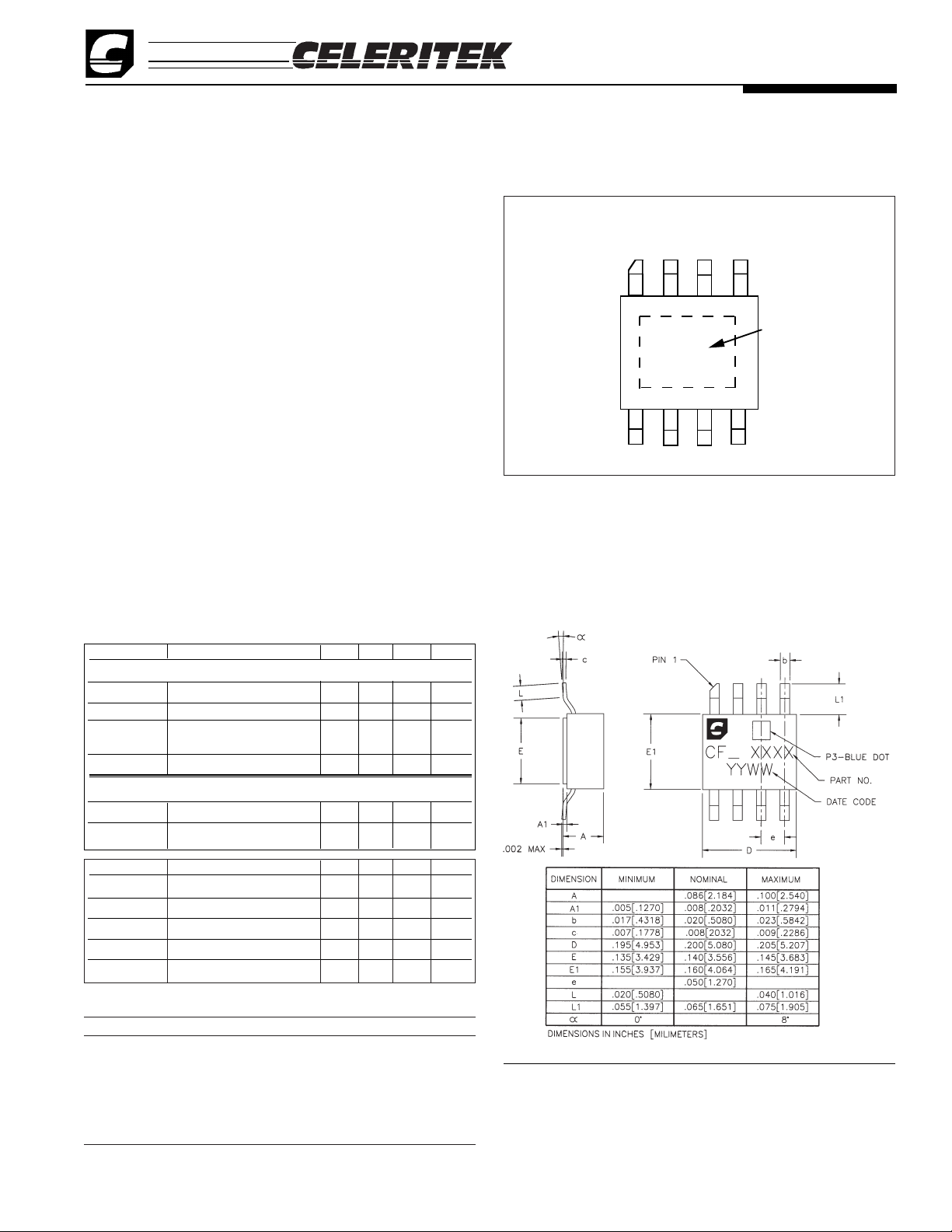
Package Diagram
Absolute Maximum Ratings
Parameter Symbol Rating
Drain-Source Voltage V
DS
10V
(3)
Gate-Source Voltage V
GS
-5V
Drain Current I
DS
Idss
Continuous Dissipation P
T
6W
Channel Temperature T
CH
175°C
Storage Temperature T
STG
-65°C to +175°C
SO-8 Power Package Physical Dimensions
Notes:
1. Sum to two tones with 1 MHz spacing = 25 dBm.
2. See thermal considerations information on page 4.
3. Maximum potential difference across the device (Vd + Vg) cannot
exceed 12V.
Parameters Conditions Min Typ Max Units
Vd= 8V, Id= 400 mA (Quiescent)
P
-1dB
30.0 31.0 — dBm
SSG 13.5 14.5 — dB
3rd Order
Products
(1)
— 30 — dBc
Efficiency @ P1dB — 40 — %
Vd= 5V, Id= 600 mA (Quiescent)
P
-1dB
— 30.5 — dBm
SSG — 13.5 — dB
Specifications (TA= 25°C) The following specifications are
guaranteed at room temperature in Celeritek test fixture at 1.95 GHz.
Parameters Conditions Min Typ Max Units
g
m
Vds = 2.0V, Vgs = 0V — 650 — mS
I
dss
Vds = 2.0V, Vgs = 0V — 1.4 — A
V
p
Vds = 3.0V, Ids = 25 mA — -1.8 Volts
BV
GD
Igd = 2.5 mA 15 17 — Volts
ΘJL(2) @150°C TCH — 12 — °C/W
3236 Scott Boulevard, Santa Clara, California 95054
Phone: (408) 986-5060 Fax: (408) 986-5095
CFK2062-P3
Product Specifications - July 1997
(2 of 4)
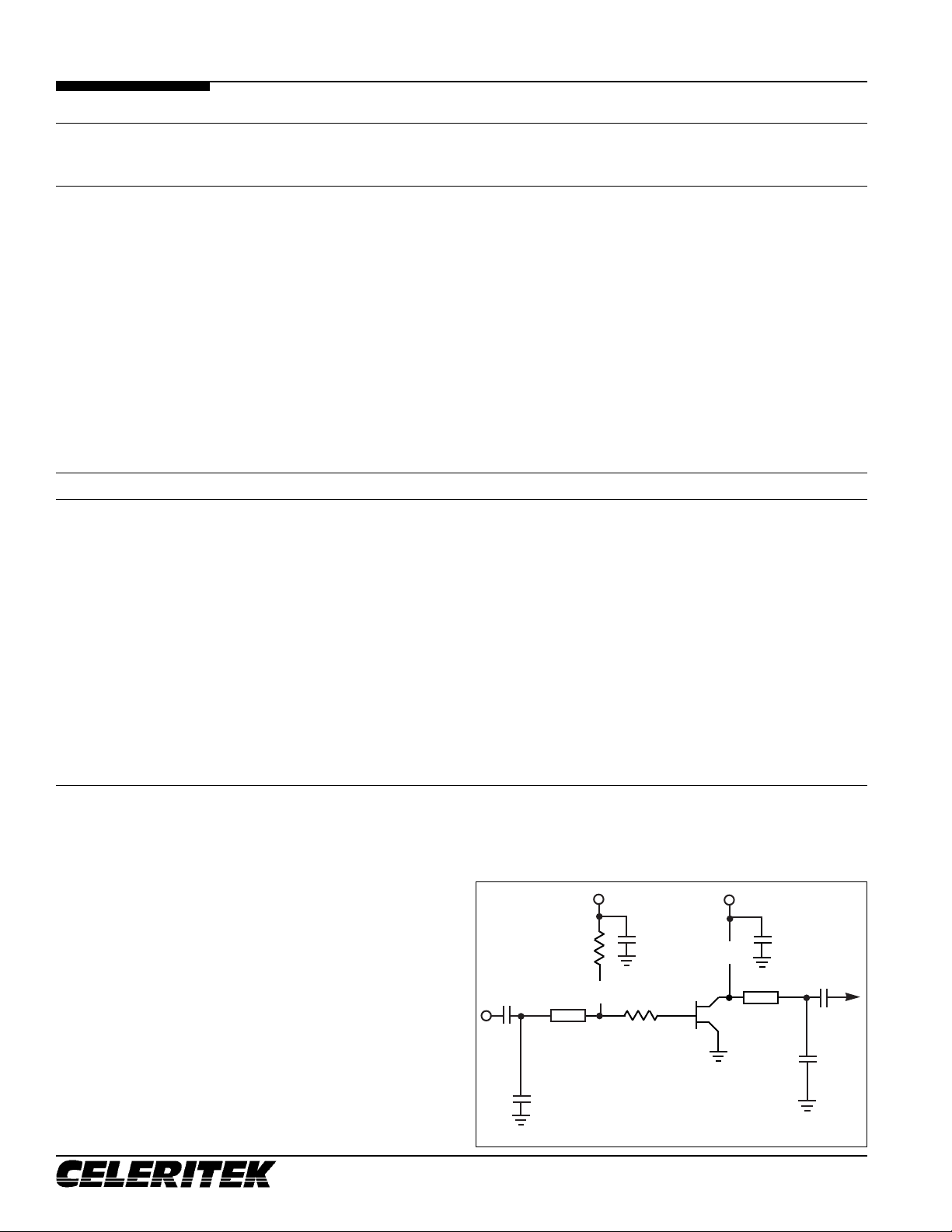
RF Match Data shown in the performance graphs was taken
in the test circuit shown at right. Layout is important for proper operation. Phase length of input and output 50Ω line varies
as a function of exact desired frequency of operation. Output
shunt inductor effects output performance. Celeritek recommends the use of a high impedance printed inductor
Lambda/4 in length. Please contact the factory for an evaluation board and/or more detailed application support.
Typical Scattering Parameters (TA= 25°C, Vds = 5 V, Ids = 600 mA)
Frequency S
11
S
21
S
12
S
22
(GHz) Mag Ang Mag Ang Mag Ang Mag Ang
0.6 0.927 -129.75 8.7 102.7 0.024 21.95 0.576 -178.45
1.0 0.914 -154.69 5.449 84.82 0.025 8.72 0.6 175.04
1.3 0.908 -162.37 4.423 76.85 0.027 4.79 0.588 172.66
1.4 0.904 -164.19 4.225 74.15 0.028 2.63 0.578 171.66
1.5 0.9 -166.3 4.066 71.35 0.029 2.62 0.567 170.4
1.6 0.897 -168.59 3.947 68.38 0.03 -0.23 0.555 168.55
1.7 0.893 -171.31 3.847 65.08 0.032 -1.99 0.542 166.26
1.8 0.889 -174.42 3.768 61.32 0.033 -5.24 0.53 163.11
1.9 0.866 -178.39 3.693 57.12 0.035 -8.52 0.52 159.17
2.0 0.883 177.09 3.605 52.62 0.05 -10.6 0.512 154.61
2.1 0.78 171.92 3.504 48.01 0.035 -14.75 0.508 149.35
2.2 0.879 166.48 3.386 42.82 0.036 -18.18 0.509 143.77
3.0 0.917 135.01 2.081 13.19 0.03 -41.27 0.623 118.42
3.5 0.932 137.14 1.635 8.18 0.028 -41.69 0.643 124.18
4.0 0.913 143.42 1.641 3.36 0.032 -41.15 0.557 131.38
(TA = 25°C, Vds = 8 V, Ids = 400 mA)
0.6 0.91 -131.25 9.129 100.5 0.026 17.07 0.521 -174.04
1.0 0.904 -155.33 5.68 82.61 0.027 6.34 0.548 178.8
1.3 0.899 -167.2 4.574 74.6 0.028 0.5 0.538 176.86
1.4 0.897 -164.68 4.366 71.76 0.029 1.6 0.53 176.13
1.5 0.892 -166.63 4.203 68.96 0.03 -0.36 0.519 174.97
1.6 0.891 -168.82 4.063 65.99 0.031 -3.35 0.507 173.4
1.7 0.886 -171.54 3.951 62.5 0.032 -4.87 0.496 171.26
1.8 0.883 -174.77 3.86 58.87 0.034 -7.72 0.483 168.5
1.9 0.88 -178.6 3.783 54.83 0.034 -9.68 0.472 164.9
2.0 0.877 176.74 3.696 50.36 0.035 -13.77 0.463 160.21
2.1 0.873 171.86 3.589 45.5 0.036 -16.17 0.458 154.9
2.2 0.874 166.29 3.46 40.56 0.037 -21.9 0.458 149.35
3.0 0.915 135.06 2.136 10.26 0.031 -46.6 0.579 121.99
3.5 0.93 137.37 1.662 4.59 0.027 -43.86 0.611 128.44
4.0 0.912 143.75 1.642 -0.35 0.031 -43.95 0.541 137.64
RF
OUT
RF
IN
CFK2062-P3, 8V, 400 mA
50 Ω
uuuu
V
g
uuuu
100 pF
50 Ω
0.1 µF
2.4 Ω
0.1 µF
91 Ω
100
pF
V
d
2.7 pF
3.9 pF
47 nH
100 nH
 Loading...