

CELER CFB0303 Datasheet
3236 Scott Boulevard Santa Clara, California 95054 Phone: (408) 986-5060 Fax: (408) 986-5095
CFB0303
Features
❏ Low-Noise Figure from 0.8 to 2.0 GHz
❏ High Gain
❏ High Intercept Point
❏ Highly Stable
❏ Easily Matched to 50Ω
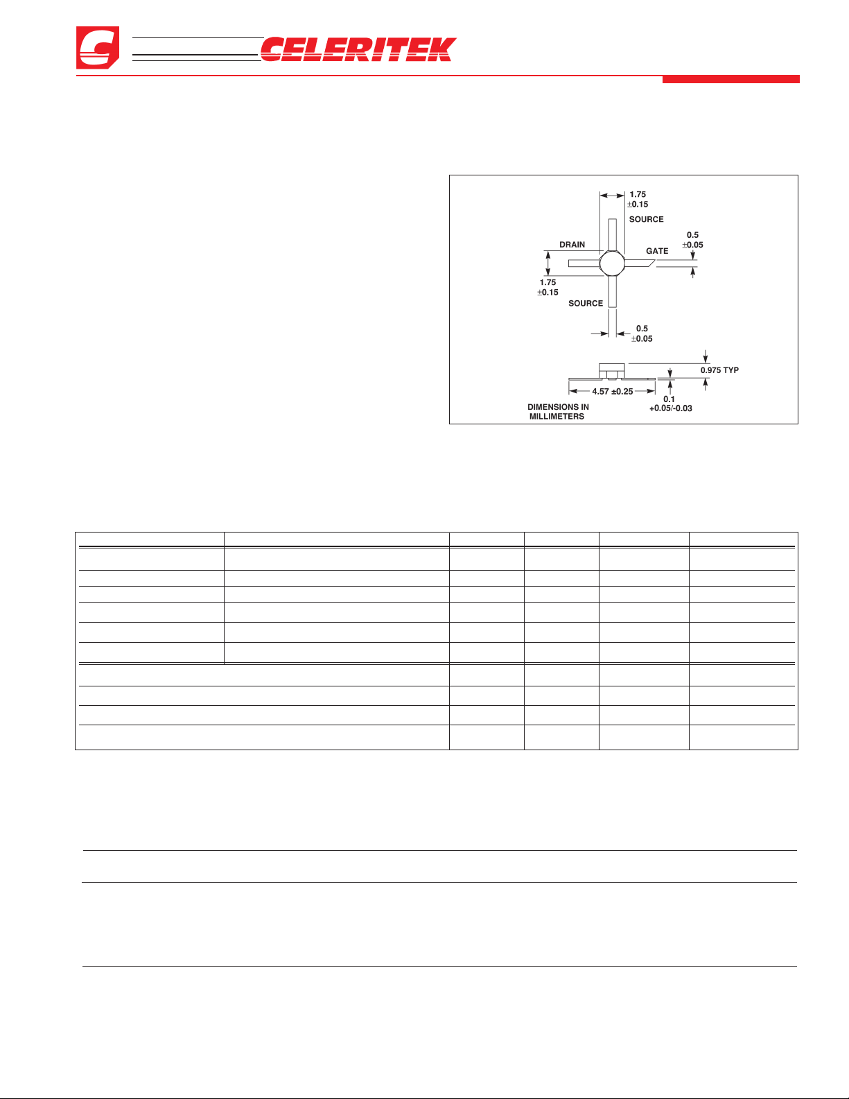
❏ 70 mil Package
❏ PHEMT Material
Applications
❏ Cellular Base Stations
❏ PCS Base Stations
❏ Industrial Data Networks
Description
Celeritek’s CFB0303 is a high performance GaAs
PHEMT with 600 µm gate width and 0.25 µ m gate length.
The low noise figure and high intercept point of this device
makes it well suited for use as the low-noise amplifier of the
High Dynamic Range
Low-Noise GaAs FET
Advanced Product Information
June 2002 (1 of 2)
base station receiver in PCS, Japanese PHS, AMPS, GSM and
other communications systems. The CFB0303 is in an industry-standard 70 mil package. It is surface mountable and
available in tape and reel.
Electrical Specifications (TA = 25°C, 2 GHz)
Parameters Conditions Min Typ Max Units
Vd= 4V, Id= 75 mA
Noise Figure
2
0.5 0.6 dB
Associated Gain
2
@ Noise Figure 19.0 20.0 22.7 dB
P
out
1, 3
P
-1
20.0 21.0 22.0 dBm
IP
3
3
+5 dBm P
OUT
/Tone 32 34 dBm
I
d
3
@ P
-1
83 mA
Transconductance Vds= 4 V, Vgs= 0 V 350 mho
Saturated Drain Current Vds= 4 V, Vgs= 0 V 80 140 240 mA
Pinchoff Voltages Vds= 4 V, Ids= 1 mA -0.3 V
Thermal Resistance @ T
case
= 150°C liquid crystal test 200 °C/W
Notes:
1. @ T
case
= 25°C. Derate 5 mW/°C for T
case
>25°C.
2. Input matched for low noise.
3. Matched for power transfer.
Typical Scattering Parameters (TA = 25°C, V
DS
= 4 V, IDS= 75 mA)
Frequency
S
11
S
21
S
12
S
22
(GHz) Mag Ang Mag (dB) Ang MAG (dB) ANG MAG ANG
0.5 0.98 -24 8.47 160 0.02 77 0.33 -9
1.0 0.94 -44 8.20 147 0.03 69 0.32 -15
2.0 0.85 -80 7.30 118 0.05 51 0.27 -36
3.0 0.76 -112 6.30 94 0.07 37 0.25 -50
4.0 0.70 -134 5.60 74 0.08 29 0.24 -55
5.0 0.64 -154 5.13 54 0.09 19 0.23 -61

3236 Scott Boulevard, Santa Clara, California 95054
Phone: (408) 986-5060 Fax: (408) 986-5095
Absolute Maximum Ratings
Parameter Symbol Rating
Drain-Source Voltage V
ds
+8V
Gate-Source Voltage V
gs
-5V
Drain Current I
ds
Idss
Continuous Dissipation
1
Pt 750 mW
Channel Temperature Tch 175°C
Storage Temperature Tstg -65°C to +150°C
CFB0303
Advanced Product Information - June 2002
(2 of 2)
Celeritek reserves the right to make changes without further notice to any products herein. Celeritek makes no warranty, representation or guarantee regarding the
suitability of its products for any particular purpose, nor does Celeritek assume any liability arising out of the application or use of any product or circuit, and specifically
disclaims any and all liability, including without limitation consequential or incidental damages. “Typical” parameters can and do vary in different applications. All operating
parameters, including “Typicals” must be validated for each customer application by customer’s technical experts. Celeritek does not convey any license under its patent
rights nor the rights of others. Celeritek products are not designed, intended, or authorized for use as components in systems intended for surgical implant into the body, or
other applications intended to support or sustain life, or for any other application in which the failure of the Celeritek product could create a situation where personal injury
or death may occur. Should Buyer purchase or use Celeritek products for any such unintended or unauthorized application, Buyer shall indemnify and hold Celeritek and
its officers, employees, subsidiaries, affiliates, and distributors harmless against all claims, costs, damages, and expenses, and reasonable attorney fees arising out of,
directly or indirectly, any claim of personal injury or death associated with such unintended or unauthorized use, even if such claim alleges that Celeritek was negligent
regarding the design or manufacture of the part. Celeritek is a registered trademark of Celeritek, Inc. Celeritek, Inc. is an Equal Opportunity/Affirmative Action Employer.
Typical Noise Parameters (V
ds
= 4 V, Ids= 75 mA)
Frequency F
min
1
Gamma Opt
(GHz) (dB) Mag Ang Rn/50
0.8 0.4 0.6 27 0.19
1.0 0.4 0.6 29 0.17
1.2 0.4 0.6 32 0.18
1.4 0.4 0.6 35 0.18
1.6 0.4 0.5 38 0.17
1.8 0.4 0.5 41 0.16
2.0 0.5 0.5 45 0.15
2.2 0.5 0.5 49 0.15
2.4 0.5 0.5 54 0.14
2.6 0.5 0.5 60 0.13
Note: 1. Fmin values reflect the circuit losses in the test fixture when
matched to optimum noise figure.
Notes
 Loading...