

CELER CFB0301 Datasheet
3236 Scott Boulevard Santa Clara, California 95054 Phone: (408) 986-5060 Fax: (408) 986-5095
CFB0301
Features
❏ Low-Noise Figure from 0.8 to 2.0 GHz
❏ High Gain
❏ High Intercept Point
❏ Highly Stable
❏ Easily Matched to 50Ω
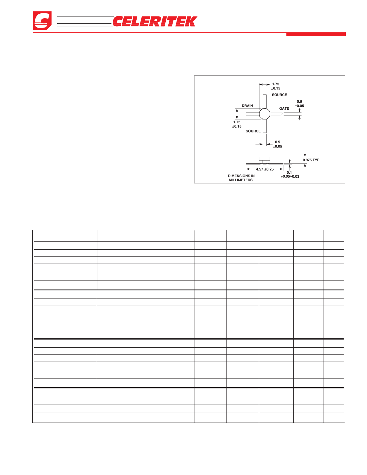
❏ 70 mil Package
Applications
❏ Cellular Base Stations
❏ PCS Base Stations
❏ Industrial Data Networks
Description
Celeritek’s CFB0301 is a high performance GaAs
MESFET with 600 µm gate width and 0.25 µ m gate length.
The low noise figure and high intercept point of this device
makes it well suited for use as the low-noise amplifier of the
High Dynamic Range
Low-Noise GaAs FET
Product Specifications
June 2002 (1 of 3)
base station receiver in PCS, Japanese PHS, AMPS, GSM and
other communications systems. The CFB0301 is in an industry-standard 70 mil package. It is surface mountable and
available in tape and reel.
Electrical Specifications (TA = 25°C, 2 GHz)
Standard
Parameters Conditions Min Typ Deviation
4
Max Units
Vd= 2V, Id= 25 mA
Noise Figure
2
0.6 dB
Associated Gain
2
@ Noise Figure 16 dB
P
out
1, 3
P
-1
15.0 dBm
IP
3
3
+5 dBm P
OUT
/Tone 24 dBm
I
d
3
@ P
-1
35 mA
Vd= 4V, Id= 30 mA
Noise Figure
2
0.7 dB
Associated Gain
2
@ Noise Figure 17 dB
P
out
1, 3
P
-1
20.5 dBm
IP
3
3
+5 dBm P
OUT
/Tone 30 dBm
I
d
3
@ P
-1
56 mA
Vd= 4V, Id= 70 mA
Noise Figure
2
0.8 0.08 0.9 dB
Associated Gain
2
@ Noise Figure 16 17 0.4 dB
P
out
1, 3
P
-1
20 21 0.4 dBm
IP
3
3
+5 dBm P
OUT
/Tone 32 34 0.9 dBm
I
d
3
@ P
-1
77 mA
Transconductance Vds= 2 V, Vgs= 0 V 70 140 mho
Saturated Drain Current Vds= 2 V, Vgs= 0 V 120 150 180 mA
Pinchoff Voltages Vds= 2 V, Ids= 1 mA -2.5 -1.3 -0.5 V
Thermal Resistance @ T
case
= 150°C liquid crystal test 200 °C/W
Notes:
1. @ T
case
= 25°C. Derate 5 mW/°C for T
case
>25°C.
2. Input matched for low noise.
3. Matched for power transfer.
4. Standard deviation based on 10 wafers randomly selected
and is provided as an estimate of the distribution only.
Trademarks are the property of their respected owners.
3236 Scott Boulevard, Santa Clara, California 95054
Phone: (408) 986-5060 Fax: (408) 986-5095
Typical Noise Parameters (V
ds
= 4 V, Ids= 30 mA)
Frequency F
min
1
Gamma Opt
(GHz) (dB) Mag Ang Rn/50
0.8 0.4 0.6 27 0.19
1.0 0.4 0.6 29 0.17
1.2 0.4 0.6 32 0.18
1.4 0.4 0.6 35 0.18
1.6 0.4 0.5 38 0.17
1.8 0.4 0.5 41 0.16
2.0 0.5 0.5 45 0.15
2.2 0.5 0.5 49 0.15
2.4 0.5 0.5 54 0.14
2.6 0.5 0.5 60 0.13
Absolute Maximum Ratings
Parameter Symbol Rating
Drain-Source Voltage V
ds
+8V
Gate-Source Voltage V
gs
-5V
Drain Current I
ds
Idss
Continuous Dissipation
1
Pt 750 mW
Channel Temperature Tch 175°C
Storage Temperature Tstg -65°C to +150°C
CFB0301
Product Specifications - June 2002
(2 of 3)
Typical Scattering Parameters (TA = 25°C, V
DS
= 2 V, IDS= 25 mA)
Frequency
S
11
S
21
S
12
S
22
(GHz) Mag Ang Mag (dB) Ang MAG (dB) ANG MAG ANG
0.5 0.98 -20 7.17 161 0.02 78 0.42 -11
1.0 0.94 -40 6.90 148 0.03 70 0.41 -24
2.0 0.85 -76 6.00 119 0.05 52 0.36 -46
3.0 0.76 -108 5.00 95 0.07 38 0.32 -65
4.0 0.70 -130 4.30 75 0.08 30 0.30 -75
5.0 0.64 -150 3.83 55 0.09 20 0.27 -85
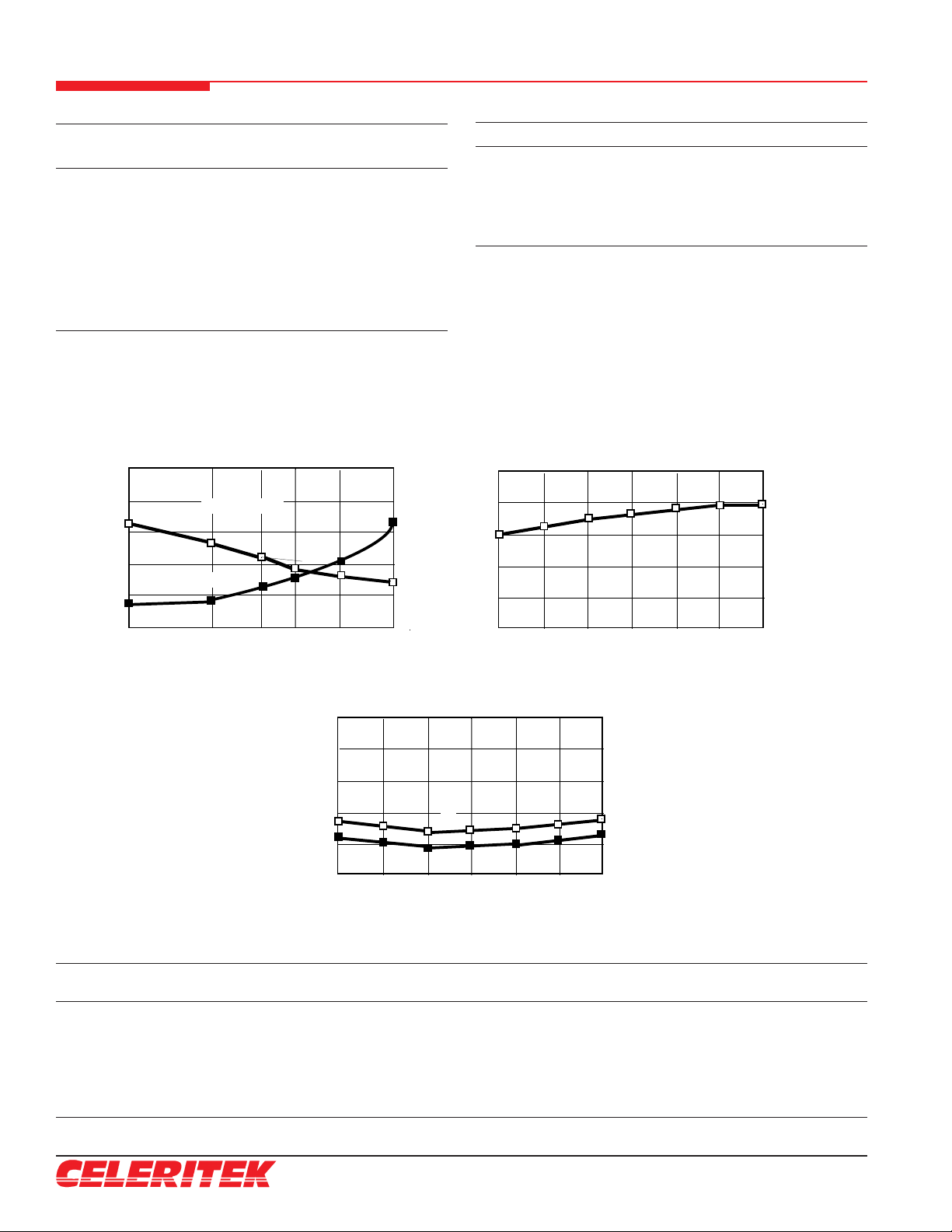
Optimum Noise Figure and Associated Gain
vs Frequency Vds = 2V, Ids = 25 mA
Frequency (GHz)
Noise Figure (dB)
246810
12
Associated Gain (dB)
Noise Figure
Associated Gain
0.5
1.0
1.5
2.0
2.50510152025
0
Optimum Noise Figure vs Ids & V
ds
Frequency = 2 GHz
Ids (mA)
Noise Figure (dB)
102030405060704V2V
0.0
0.5
1.0
1.5
2.0
2.5
Ids (mA)
Associated Gain vs I
ds
Vds = 2V, Frequency = 2 GHz
Gain (dB)
102030405060701520251050
Typical Performance
Note: 1. Fmin values reflect the circuit losses in the test fixture when
matched to optimum noise figure.
 Loading...