

Page 1
ZIC2410 Series
MeshConnect
ZICM2410-EVB3 Evaluation Board
Hardware Reference Guide
0007-05-08-03-001
(Rev C)
Page 2

ZICM2410-EVB3 Hardware Reference Guide
TableofContents
1
INTRODUCTION .............................................................................. 3
1.1 PART DEFINITIONS .................................................................................... 3
2 ZICM2410-EVB3 EVALUATION BOARD ......................................... 4
2.1 BOARD COMPONENTS ............................................................................. 4
3 MESHCONNECT ZICM2410P0 MODULE ....................................... 6
3.1 DESCRIPTION ............................................................................................ 6
3.2 ZICM2410P0 MODULE CONNECTION ....................................................... 7
3.3 ZICM2410P2 MODULE CONNECTION ..................................................... 10
4 ON BOARD RESOURCES ............................................................. 13
4.1 POWER SUPPLY ....................................................................................... 13
4.2 RESET ....................................................................................................... 13
4.3 ISP SWITCH .............................................................................................. 13
4.4 POWER HEADER (J4) .............................................................................. 14
4.5 LEDS .......................................................................................................... 14
4.6 PUSHBUTTON SWITCHES ...................................................................... 15
4.7 EXTERNAL MEMORY ............................................................................... 15
4.8 VOICE CODEC .......................................................................................... 15
4.9 HEADPHONE / MICROPHONE JACKS .................................................... 15
4.10 ADDITIONAL JUMPER FUNCTIONS/CONNECTIONS ............................ 16
5 REVISION HISTORY ...................................................................... 17
APPENDIX-1: SCHEMATIC OF ZICM2410-EVB3 ............................... 18
APPENDIX-2: BILL OF MATERIALS (ZICM2410-EVB3) .................... 19
Rev C Document No. 0007-05-08-03-001 Page 2 of 19
Page 3

ZICM2410-EVB3 Hardware Reference Guide
1 INTRODUCTION
This document describes the hardware, features and functions of the CEL ZICM2410-EVB3
Evaluation Board, one of the major hardware components in the CEL ZICM2410P0-KIT2
evaluation kit. At the heart of the evaluation board is the ZICM2410P0 (or ZICM2410P2), CEL’s
transceiver module solution for IEEE 802.15.4 wireless applications.
1.1 PART DEFINITIONS
ZIC2410QN48: CEL MeshConnect single-chip IEEE 802.15.4 transceiver.
ZICM2410P0: CEL MeshConnect IEEE 802.15.4 module.
ZICM2410P2: CEL MeshConnect Extended Range IEEE 802.15.4 module with an
external power amplifier.
ZICM2410-EVB3: An evaluation board containing a ZICM2410P0-1 for development
and evaluation purposes. Using the CEL supplied software tools makes it possible to
download user-created programs to the ZIC2410.
ZICM2410P0-KIT2: CEL MeshConnect IEEE 802.15.4 evaluation kit.
ZIC2410: Same as the ‘ZIC2410QN48’.
Rev C Document No. 0007-05-08-03-001 Page 3 of 19
Page 4
ZICM2410-EVB3 Hardware Reference Guide
2 ZICM2410-EVB3 EVALUATION BOARD
CAUTION
The ZICM2410-EVB3 is a PC interface board to which the ZICM2410P0 / ZICM2410P2 module
has been mounted. A ZICM2410-EVB3 can be used to interface PC applications with the
module, in order to program user applications to the ZICM2410.
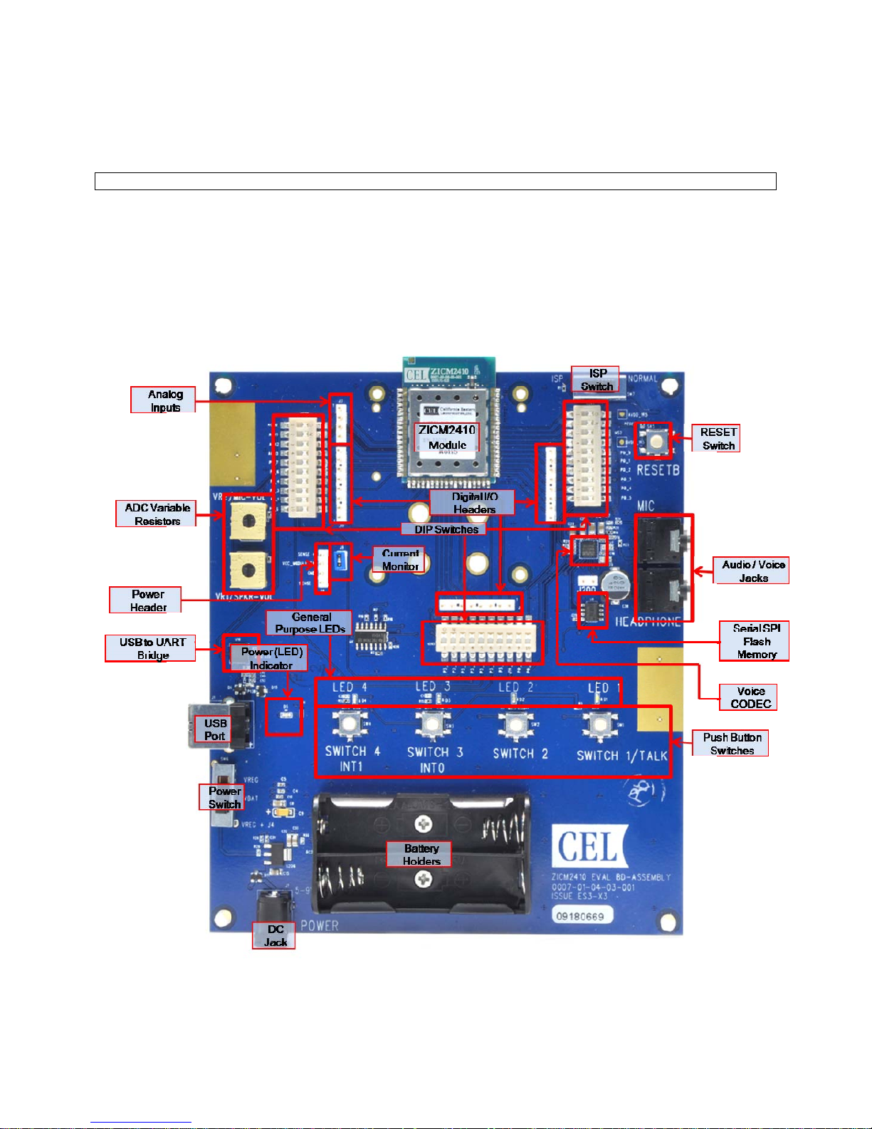
Figure 1 shows the ZICM2410-EVB3 evaluation board, the major components of which are
described in Table 1.
: Contains parts and assemblies susceptible to damage by Electrostatic Discharge (ESD)
2.1 BOARD COMPONENTS
Figure 1 – Photo, ZICM2410-EVB3 Evaluation Board
Rev C Document No. 0007-05-08-03-001 Page 4 of 19
Page 5

ZICM2410-EVB3 Hardware Reference Guide
Table 1 – ZICM2410-EVB3 Descriptions / Functions of the Major Components
Components Description / Function
Audio / Voice Jacks
ZICM2410
Module
DIP Switches
Microphone input and Headphone output for connection when using the evaluation
board’s voice / audio features.
ZICM2410
module. The DUT of the evaluation board
3 ea 10-pin DIP Switches used for disconnecting the evaluation boards connections
to the various on board features (i.e. LEDs, switches, etc.).
ISP Mode Switch: 2-position slide switch to control ISP mode
ISP Switch
‘ISP’ position is used for downloading application firmware to the ZICM2410.
For normal operation, the switch should be set to the ‘NORMAL’ position.
RESET Switch Button switch to reset the device MPU (Active Low)
General Purpose LEDs Four indicator LEDs for GPIO output tests
Push Button Switches connected to General Purpose I/O (GPIO) Ports:
Test Tact Switches
When a button is pressed, the signal ‘0’ is applied to the corresponding port pin;
otherwise, a value of ‘1’ is applied. Switches #3 and #4 can be configured as
external interrupts to the 8051 microcontroller.
Battery Holders Holder for 2 ea. 1.5 Volt Type AA Batteries
DC JACK Input for a 5.0 – 9.0 Volt DC Power Supply
This three position slide switch is used to select the power source for the evaluation
POWER Switch
board. In the position ‘VREG’, power is supplied either through the USB port or from
a power supply inserted in the DC Jack. In the ‘VBAT’ position, batteries provide the
power.
Power Indicator LED LED indicates when DC power is turned on.
USB Port Port to connect the evaluation board through a USB cable to a PC.
ADC Variable Resistors Variable Resistors for testing ADC functions in the
ZICM2410
module
Current Monitor For measuring operating current of the module under various conditions
USB to UART Bridge Silicon Labs CP2102 USB to UART Bridge IC: Converts I/O from USB to UART.
Analog Inputs
Digital I/O Headers
1 ea. 4-pin header to provide a convenient method to monitor or connect to an
Analog input.
3 ea. 8-pin header to provide a convenient method for to monitor or connect to a
selected Digital GPIO port.
SPI Flash Memory Onboard ROM for storing additional information.
Voice CODEC Onboard Voice CODEC used for A/D and D/A conversions of Voice / Audio.
Power Header 4-pin header for direct powering of the EVB, bypassing the internal regulator
Rev C Document No. 0007-05-08-03-001 Page 5 of 19
Page 6
ZICM2410-EVB3 Hardware Reference Guide
3 MeshConnect ZICM2410P0 MODULE
CAUTION
The ZICM2410P0 / ZICM2410P2 module is the primary active component/device under test of
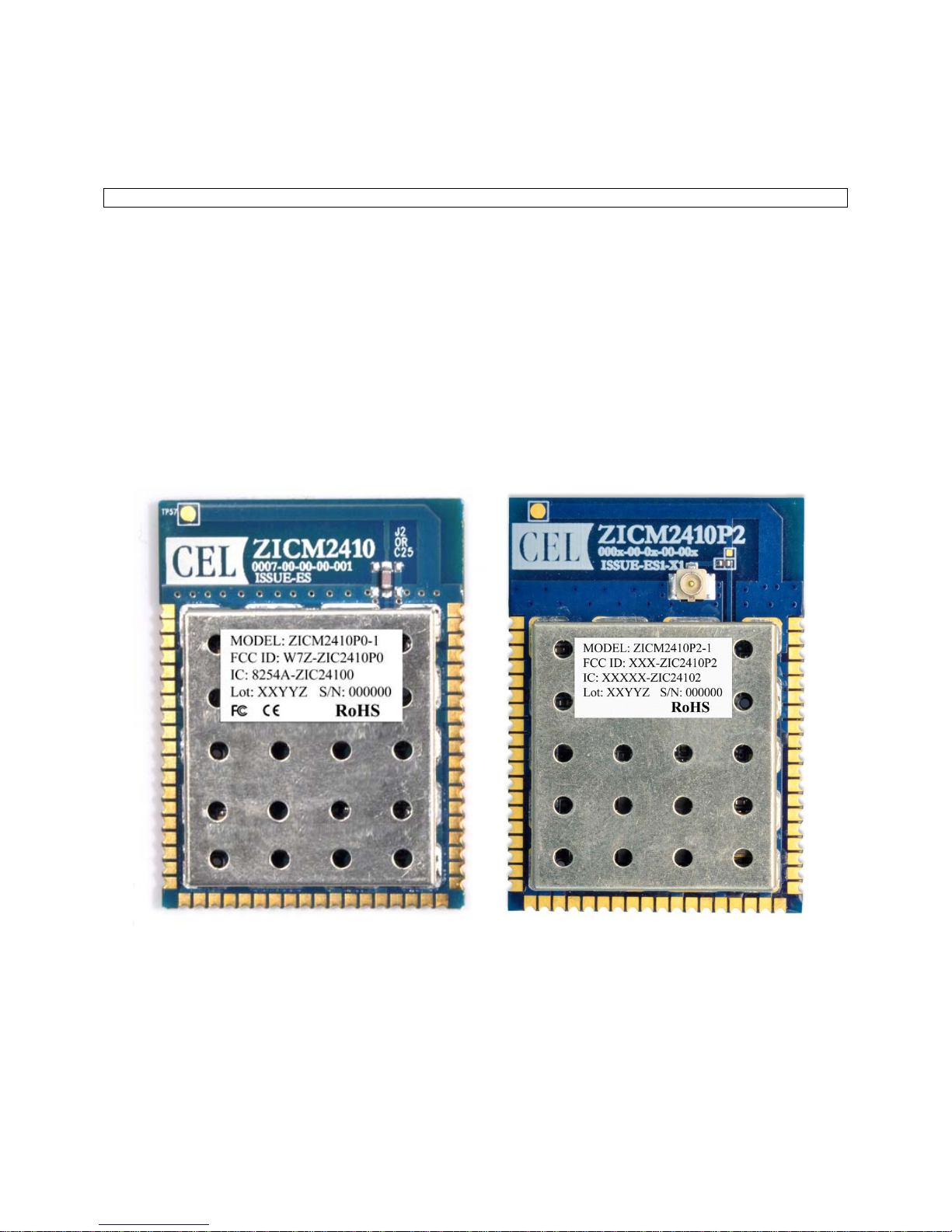
the ZICM2410-EVB3 evaluation board. Figure 2 shows the ZICM2410P0 / ZICM2410P2
modules, whose major components are as follows:
ZIC2410QN48
Power Amplifier and Low Noise Amplifier (only found on the ZICM2410P2)
16MHz Crystal
Integrated PCB Trace antenna (or optional U.FL connector for an external antenna)
Additional components for RF matching and termination
: Contains parts and assemblies susceptible to damage by Electrostatic Discharge (ESD)
3.1 DESCRIPTION
Figure 2 – Photo, ZICM2410P0 / ZICM2410P2 Modules
Rev C Document No. 0007-05-08-03-001 Page 6 of 19
Page 7
ZICM2410-EVB3 Hardware Reference Guide
3.2 ZICM2410P0 MODULE CONNECTION
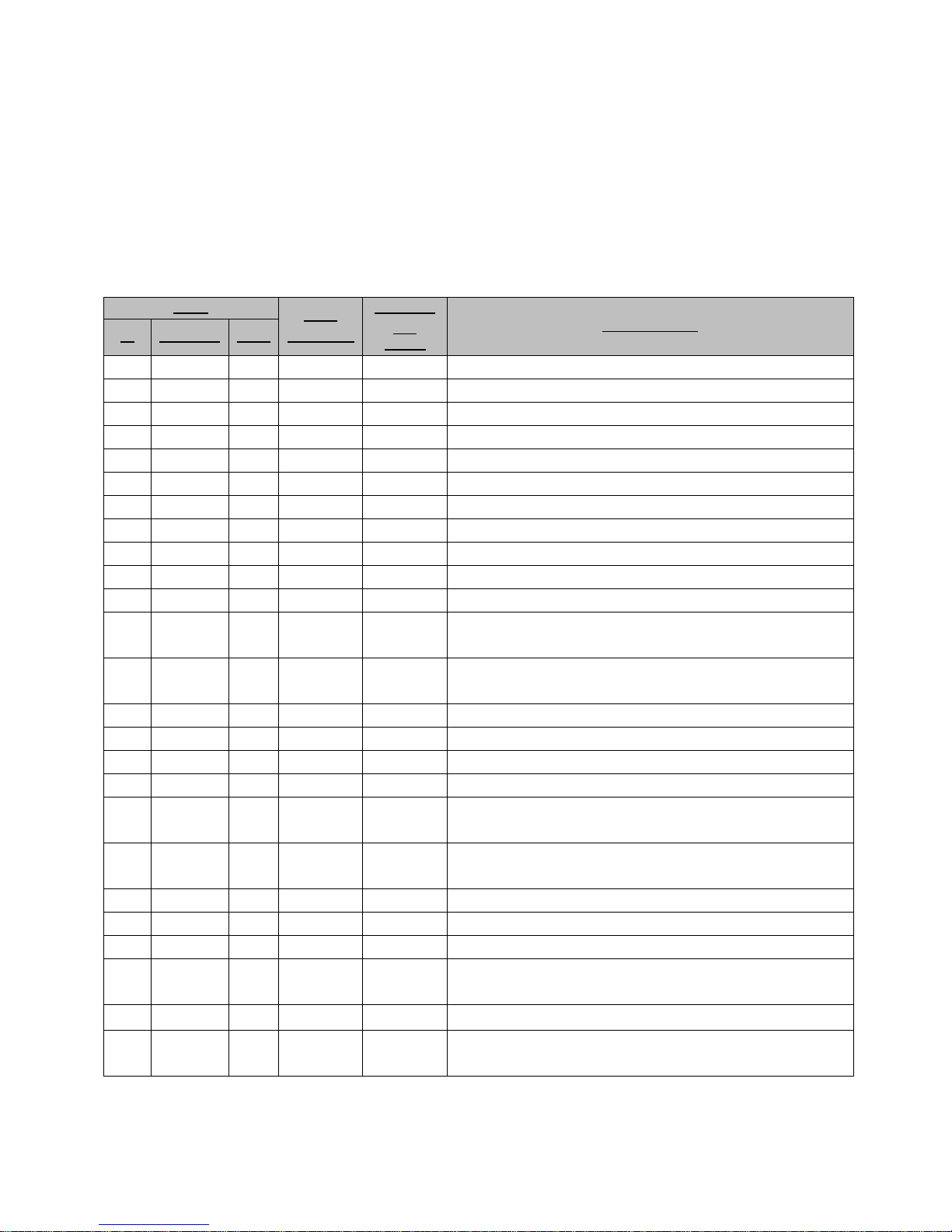
Table 2, Table 3 and Table 4 describe the ZICM2410P0 module pins and their connection to the
DIP switches, which can be used for isolation (to disconnect the evaluation board from the
ZICM2410P0). Also listed is the ZIC2410 (discrete IC) pin number. The tables also indicate the
default settings of the isolation DIP switches (U203, U204 and U205) for operation with the preprogrammed application. All module GND pins are physically hardwired to ground.
Table 2 – ZICM2410 / EVB3 Connections, U204
PIN #
IC MODULE U204
U204
POSITION
PAD 1 GND4 Connected to Ground.
PAD 2 GND3 Connected to Ground.
14 3 MS1 Connected to Ground.
PAD 4 GND0 Connected to Ground.
13 5 MS0 Connected to Ground.
6 NC2 No Connection.
PAD 7 GND20 Connected to Ground.
PAD 8 GND12 Connected to Ground.
PAD 9 GND13 Connected to Ground.
PAD 10 GND17 Connected to Ground.
PAD 11 GND5 Connected to Ground.
8 12 1 ON ACH0
9 13 2 ON ACH1
10 14 3 ON ACH2 ADC Input, Channel #2.
11 15 4 ON ACH3 ADC Input, Channel #3.
20 16 5 ON P1_7 GPIO P1.7
21 17 6 ON P1_6 GPIO P1.6
22 18 7 ON P1_4
23 19 8 ON P1_3
PAD 20 GND9 Connected to Ground.
PAD 21 GND8 Connected to Ground.
PAD 22 GND7 Connected to Ground.
24 23 9 ON P1_1
7 24 VCC_3V
26 25 10 ON P1_0
MODULE
PIN
NAME
DESCRIPTION
ADC Input, Channel #0.
When U204:1 “ON” - Connected to VR1 on EVB3
ADC Input, Channel #1.
When U204:2 “ON” - Connected to VR2 on EVB3
GPIO P1.4
When U204:7 “ON” - Connected to SW2 on EVB3
GPIO P1.3
When U204:8 “ON” - Connected to SW1 on EVB3
GPIO P1.1
When U204:9 “ON” - Connected to USB_RX on EVB3
Power Supply Input, See Section
4.1.
GPIO P1.0
When U204:10 “ON” - Connected to USB_TX on EVB3
Rev C Document No. 0007-05-08-03-001 Page 7 of 19
Page 8

ZICM2410-EVB3 Hardware Reference Guide
Table 3 - ZICM2410 / EVB3 Connections, U205
PIN #
IC MODULE
27 26 1 ON P3_7
28 27 2 ON P3_6
29 28 3 ON P3_5
30 29 4 ON P3_4
30 GND10 Connected to Ground.
31 31 5 ON P3_3
32 32 6 ON P3_2
33 GND11 Connected to Ground.
33 34 7 ON P3_1
35 35 8 ON P3_0
36 GND6 Connected to Ground.
36 37 9 ON P0_7
37 38 10 ON P_06
U205
U205
POSITION
MODULE
PIN
NAME
GPIO P3.7
When U205:1 “ON” - Connected to SPI Bus on EVB3
GPIO P3.6
When U205:2 “ON” - Connected to SPI Bus on EVB3
GPIO P3.5
When U205:3 “ON” - Connected to SPI Bus on EVB3
GPIO P3.4
When U205:4 “ON” - Connected to SPI Bus on EVB3
GPIO P3.3
When U205:5 “ON” - Connected to SW4 on EVB3
GPIO P3.2
When U205:6 “ON” - Connected to SW3 on EVB3
GPIO P3.1
When U205:7 “ON” - Connected to SPI Bus on EVB3
GPIO P3.0
When U205:8 “ON” - Connected to LED4 on EVB3
GPIO P0.7
When U205:9 “ON” - Connected to I2S Bus on EVB3
GPIO P0.6
When U205:10 “ON” - Connected to I2S Bus on EVB3
DESCRIPTION
Rev C Document No. 0007-05-08-03-001 Page 8 of 19
Page 9

ZICM2410-EVB3 Hardware Reference Guide
Table 4 - ZICM2410 / EVB3 Connections, U203
PIN #
IC MODULE
U203
38 39 10 ON P0_5
39 40 9 ON P0_4
40 41 8 ON P0_3
41 42 7 ON P0_2
42 43 6 ON P0_1
43 44 5 ON P0_0
U203
POSITION
MODULE
PIN NAME
DESCRIPTION
GPIO P0.5
When U203:10 “ON” - Connected to I2S Bus on EVB3
GPIO P0.4
When U203:9 “ON” - Connected to I2S Bus on EVB3
GPIO P0.3
When U203:8 “ON” - Connected to LED1 on EVB3
GPIO P0.2
When U203:7 “ON” - Connected to LED2 on EVB3
GPIO P0.1
When U203:6 “ON” - Connected to LED3 on EVB3
GPIO P0.0
When U203:5 “ON” - Connected to I2S Bus on EVB3
19 45 4 ON DVDD_1_5 1.5 Volt Regulated Output, Digital Plane.
15 46 3 ON ISP
ISP Mode Select
When U203:3 “ON” - Connected to SW7 on EVB3
17 47 2 ON RESET# When U203:2 “ON” - Connected to SW5 on EVB3
6 48 1 ON AVDD_1_5 1.5 Volt Regulated Output, Analog Plane.
49 GND14 Connected to Ground.
50 GND15 Connected to Ground.
51 GND16 Connected to Ground.
52 GND18 Connected to Ground.
53 GND19 Connected to Ground.
54 NC1 No Connection.
55 GND1 Connected to Ground.
56 GND2 Connected to Ground.
Rev C Document No. 0007-05-08-03-001 Page 9 of 19
Page 10
ZICM2410-EVB3 Hardware Reference Guide
3.3 ZICM2410P2 MODULE CONNECTION
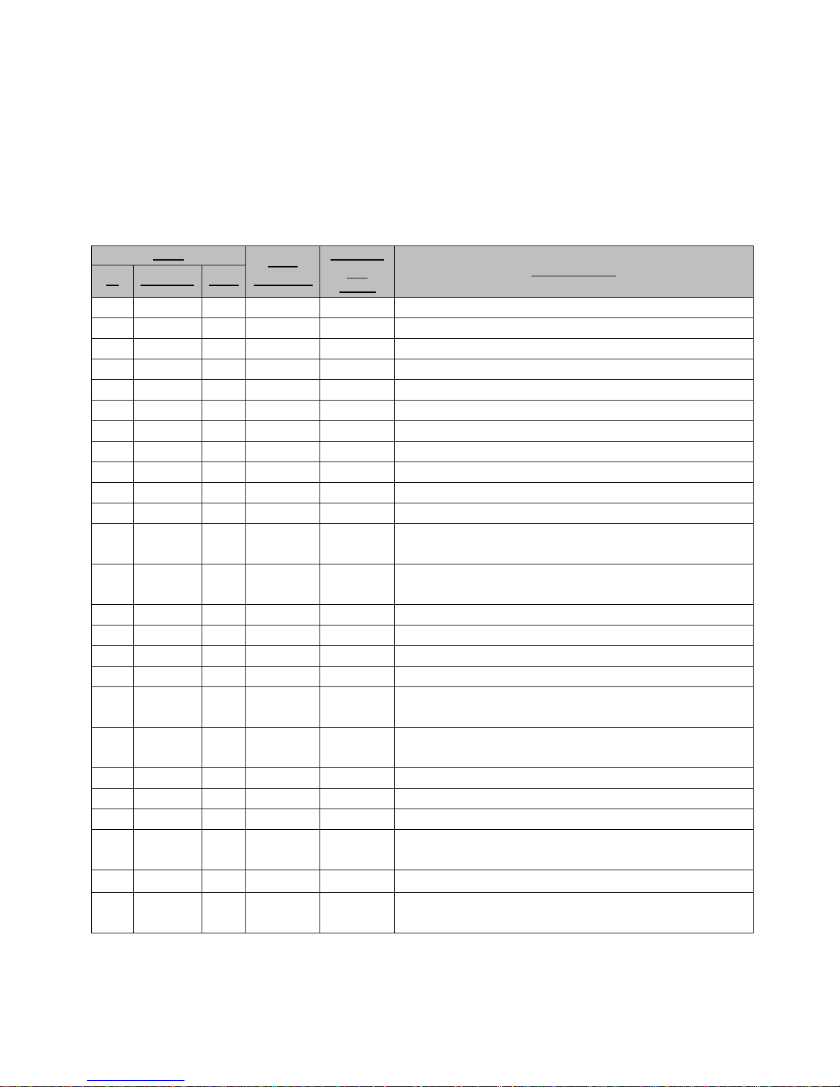
Table 5, Table 6 and Table 7 describe the ZICM2410P2 module pins and their connection to the
DIP switches, which can be used for isolation (to disconnect the evaluation board from the
ZICM2410P2). Also listed is the ZIC2410 (discrete IC) pin number. The tables also indicate the
default settings of the isolation DIP switches (U203, U204 and U205) for operation with the preprogrammed application. All module GND pins are physically hardwired to ground.
Table 5 – ZICM2410 / EVB3 Connections, U204
PIN #
IC MODULE U204
U204
POSITION
PAD 1 GND4 Connected to Ground.
PAD 2 GND3 Connected to Ground.
14 3 MS1 Connected to Ground.
PAD 4 GND0 Connected to Ground.
13 5 MS0 Connected to Ground.
6 NC2 No Connection.
PAD 7 GND20 Connected to Ground.
PAD 8 GND12 Connected to Ground.
PAD 9 GND13 Connected to Ground.
PAD 10 GND17 Connected to Ground.
PAD 11 GND5 Connected to Ground.
8 12 1 ON ACH0
9 13 2 ON ACH1
10 14 3 ON ACH2 ADC Input, Channel #2.
11 15 4 ON ACH3 ADC Input, Channel #3.
20 NC3 No Connection.
21 NC4 No Connection.
22 18 7 ON P1_4
23 19 8 ON P1_3
PAD 20 GND9 Connected to Ground.
PAD 21 GND8 Connected to Ground.
PAD 22 GND7 Connected to Ground.
24 23 9 ON P1_1
7 24 VCC_3V
26 25 10 ON P1_0
MODULE
PIN
NAME
DESCRIPTION
ADC Input, Channel #0.
When U204:1 “ON” - Connected to VR1 on EVB3
ADC Input, Channel #1.
When U204:2 “ON” - Connected to VR2 on EVB3
GPIO P1.4
When U204:7 “ON” - Connected to SW2 on EVB3
GPIO P1.3
When U204:8 “ON” - Connected to SW1 on EVB3
GPIO P1.1
When U204:9 “ON” - Connected to USB_RX on EVB3
Power Supply Input, See Section
4.1.
GPIO P1.0
When U204:10 “ON” - Connected to USB_TX on EVB3
Rev C Document No. 0007-05-08-03-001 Page 10 of 19
Page 11

ZICM2410-EVB3 Hardware Reference Guide
Table 6 - ZICM2410 / EVB3 Connections, U205
PIN #
IC MODULE
27 26 1 ON P3_7
28 27 2 ON P3_6
29 28 3 ON P3_5
30 29 4 ON P3_4
30 GND10 Connected to Ground.
31 31 5 ON P3_3
32 32 6 ON P3_2
33 GND11 Connected to Ground.
33 34 7 ON P3_1
35 35 8 ON P3_0
36 GND6 Connected to Ground.
36 37 9 ON P0_7
37 38 10 ON P_06
U205
U205
POSITION
MODULE
PIN
NAME
GPIO P3.7
When U205:1 “ON” - Connected to SPI Bus on EVB3
GPIO P3.6
When U205:2 “ON” - Connected to SPI Bus on EVB3
GPIO P3.5
When U205:3 “ON” - Connected to SPI Bus on EVB3
GPIO P3.4
When U205:4 “ON” - Connected to SPI Bus on EVB3
GPIO P3.3
When U205:5 “ON” - Connected to SW4 on EVB3
GPIO P3.2
When U205:6 “ON” - Connected to SW3 on EVB3
GPIO P3.1
When U205:7 “ON” - Connected to SPI Bus on EVB3
GPIO P3.0
When U205:8 “ON” - Connected to LED4 on EVB3
GPIO P0.7
When U205:9 “ON” - Connected to I2S Bus on EVB3
GPIO P0.6
When U205:10 “ON” - Connected to I2S Bus on EVB3
DESCRIPTION
Rev C Document No. 0007-05-08-03-001 Page 11 of 19
Page 12

ZICM2410-EVB3 Hardware Reference Guide
Table 7 - ZICM2410 / EVB3 Connections, U203
PIN #
IC MODULE
U203
38 39 10 ON P0_5
39 40 9 ON P0_4
40 41 8 ON P0_3
41 42 7 ON P0_2
42 43 6 ON P0_1
43 44 5 ON P0_0
U203
POSITION
MODULE
PIN NAME
DESCRIPTION
GPIO P0.5
When U203:10 “ON” - Connected to I2S Bus on EVB3
GPIO P0.4
When U203:9 “ON” - Connected to I2S Bus on EVB3
GPIO P0.3
When U203:8 “ON” - Connected to LED1 on EVB3
GPIO P0.2
When U203:7 “ON” - Connected to LED2 on EVB3
GPIO P0.1
When U203:6 “ON” - Connected to LED3 on EVB3
GPIO P0.0
When U203:5 “ON” - Connected to I2S Bus on EVB3
19 45 4 ON DVDD_1_5 1.5 Volt Regulated Output, Digital Plane.
15 46 3 ON ISP
ISP Mode Select
When U203:3 “ON” - Connected to SW7 on EVB3
17 47 2 ON RESET# When U203:2 “ON” - Connected to SW5 on EVB3
6 48 1 ON AVDD_1_5 1.5 Volt Regulated Output, Analog Plane.
49 GND14 Connected to Ground.
50 GND15 Connected to Ground.
51 GND16 Connected to Ground.
52 GND18 Connected to Ground.
53 GND19 Connected to Ground.
54 NC1 No Connection.
55 GND1 Connected to Ground.
56 GND2 Connected to Ground.
Rev C Document No. 0007-05-08-03-001 Page 12 of 19
Page 13
ZICM2410-EVB3 Hardware Reference Guide
4 ON BOARD RESOURCES
4.1 POWER SUPPLY
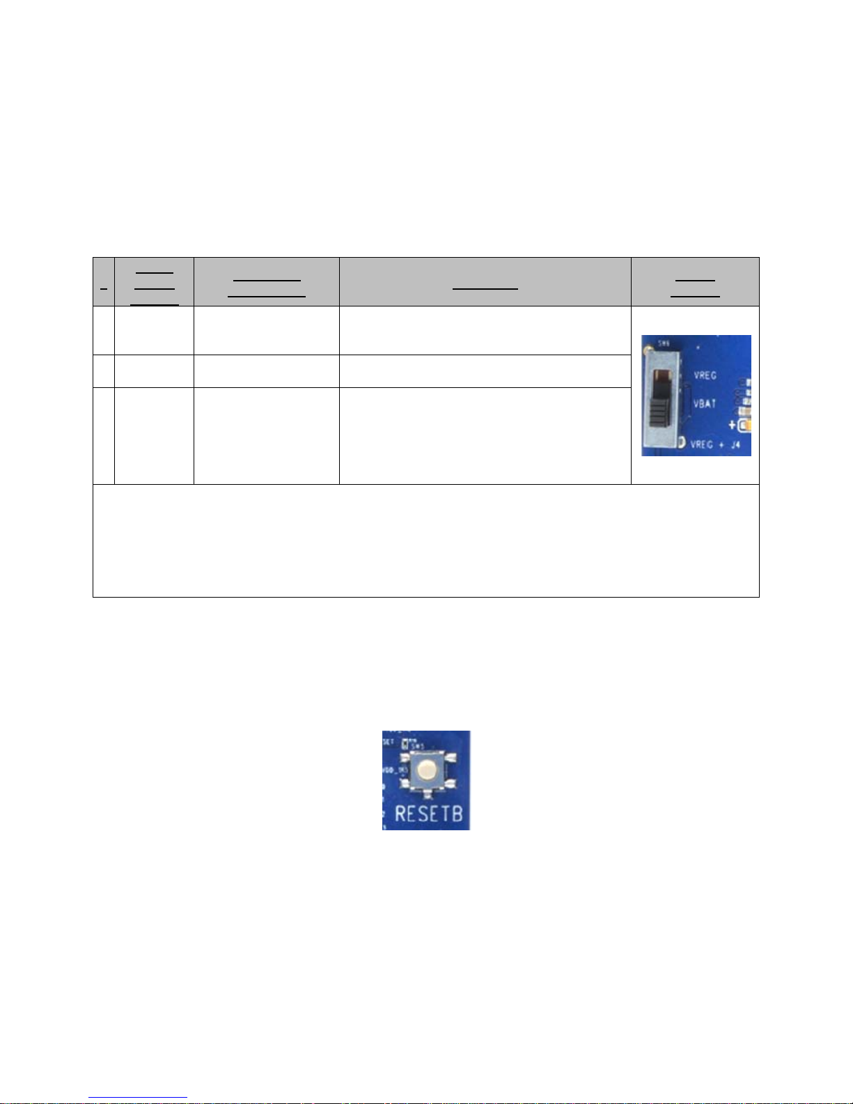
The three position slide switch (SW6) operates in accordance with the settings given in Table 8.
The Power Indicator LED (red) illuminates when power is applied to the evaluation board
through any of the methods.
Table 8 – EVB3 Power Switch Settings
Power
#
Switch
Position
1 VREG
2 VBAT 3.0 V
3 VREG + J4
NOTE #1:
all the LEDs (LED1 through LED4) are illuminated. Once the initialization routine has completed the LEDs are turned
off.
NOTE #2:
Power Switch is toggled between the VBAT and either of the VREG postions the device may get stuck in the
initialization routine. If this occurs, simply press the RESETB button.
At power-on, the evaluation board preforms an initialization routine (approximately 1 second) during which
If batteries are loaded into the holder and the board also has power applied via the USB or DC Jack, and the
VCC Power
Supply Value
VUSB: 5.0 V
DC Jack: 5.0 – 9.0 V
ZIC2410-EVB3: 5 V
ZICM2410: 2.1 – 3.0V
Comments
In this position the evaluation board and module
are either powered from the USB interface or
through the DC Jack from an external supply.
In this position the evaluation board and module
are powered from the two 1.5 V Type AA batteries.
In this position the evaluation board is powered via
either the USB interface or through the DC Jack.
The ZICM2410 module is powered externally via
the J4 header. See the
Evaluation Board Hardware Reference Guide”
for further details.
“ZICM2410-EVB3
Switch
Position
4.2 RESET
The ZICM2410-EVB3, by default, has the switch labeled ‘RESETB’ (SW5) connected to the
‘RESET#’ pin of the ZICM2410 module. When pressed, the ZIC2410 will be reset. Using the
isolation DIP switches (U203:2), SW5 can be disconnected and external circuitry added.
Figure 3 – Photo, RESETB Push Button (SW5)
4.3 ISP SWITCH
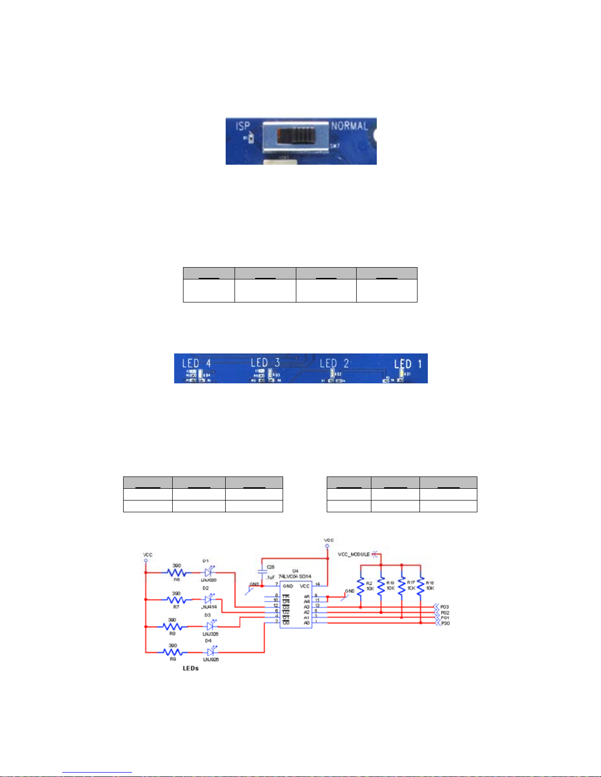
The 2-position slide switch (SW7) controls the mode of operation, as shown in Figure 4. The
ZIC2410 can be placed into either ‘ISP’ or ‘NORMAL’ mode. When placed into ISP mode, the
ZIC2410 is configured for the programming of the internal Flash memory (i.e. a firmware
upgrade). In order to enter ISP mode, the slider switch must be set to ‘ISP’ and then power
applied to the device (alternatively, if power has already been applied the ‘RESETB’ pushbutton
Rev C Document No. 0007-05-08-03-001 Page 13 of 19
Page 14
ZICM2410-EVB3 Hardware Reference Guide
may be pressed and released after the slider switch has been set). In order to return to
‘NORMAL’ mode after programming has completed, simply slide the slider switch to ‘NORMAL’
and press and release the ‘RESETB’ pushbutton.
Figure 4 – Photo, ISP Switch
4.4 POWER HEADER (J4)
This header allows the powering of the ZICM2410 module directly (bypassing the regulator)
through Pin #3 and allows the monitoring of the module’s supply line through Pin #4 (SENSE+).
Table 9 – Power Header (J4) Pin Out
Pin 1 Pin 2 Pin 3 Pin 4
GND
(SENSE–)
GND Module
(Supply)
VCC Module
(Supply)
VCC Module
(SENSE+)
4.5 LEDs
Figure 5 - Photo, LEDs
The ZICM2410-EVB3 includes four colored LEDs. They are connected to various GPIOs of the
ZICM2410 module through an inverter as shown in Figure 6. To turn on a LED, the
corresponding GPIO pin must be set high. To turn off a LED, the GPIO pin must be cleared (set
low).
Table 10 – LED Colors and Connections
LED # Color GPIO LED # Color GPIO
LED 1 White Port 0[3] LED 3 Green Port 0[1]
LED 2 Amber Port 0[2] LED 4 Blue Port 3[0]
Rev C Document No. 0007-05-08-03-001 Page 14 of 19
Figure 6 – Drawing, LEDs Schematic
Page 15
ZICM2410-EVB3 Hardware Reference Guide
4.6 PUSHBUTTON SWITCHES
Figure 7 – Photo, Pushbutton Switches
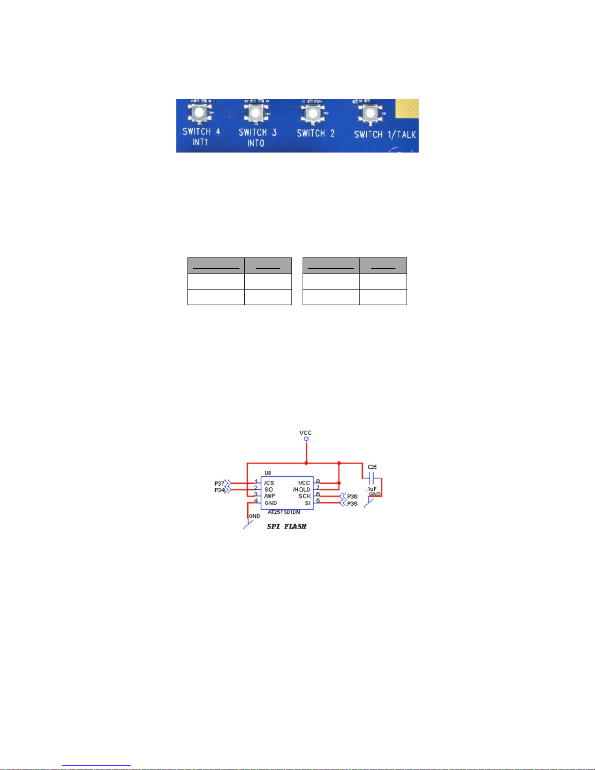
When a pushbutton switch is pressed, the corresponding GPIO is pulled low. When released
(or not pressed), the GPIO is pulled high. The pushbutton switches correspond to the GPIOs as
listed in Table 11. Switch #3 and #4 are dual purpose, as they can also be used as the External
Interrupts (INT0 and INT1) inputs for the embedded processor.
Table 11 – Pushbutton S witch Connections
SWITCH # GPIO SWITCH # GPIO
1 Port 1[3] 3 Port 3[2]
2 Port 1[4] 4 Port 3[3]
4.7 EXTERNAL MEMORY
To store non-volatile data, the ZICM2410-EVB3 provides an on-board external SPI Flash
memory connected to the Serial Peripheral Interface (SPI) of the ZIC2410. The external
memory is required when performing Over-the-Air programming. Using the isolation DIP
switches, the memory can be easily disconnected from the ZIC2410. Figure 8 details the
connection details below.
Figure 8 – Drawing, External Memory Circuit
4.8 VOICE CODEC
The ZICM2410-EVB3 has an on-board mono CODEC with speaker driver to support wireless
audio and voice. The primary purpose of the external chip is to perform the analog-to-digital
and digital-to-analog conversions. The CODEC is configured using the SPI interface while the
audio / voice data uses the ZIC2410’s I2S interface.
4.9 HEADPHONE / MICROPHONE JACKS
The ZICM2410-EVB3 is equipped with two 3.5 mm jacks, one for headphones and one for a
microphone input. The evaluation board has been optimized for headphones with 32 Ω
Rev C Document No. 0007-05-08-03-001 Page 15 of 19
Page 16

ZICM2410-EVB3 Hardware Reference Guide
impedance and single-ended microphones with 2.2 kΩ impedance.
4.10 ADDITIONAL JUMPER FUNCTIONS/CONNECTIONS
Table 12 –Functions/Connections of Other Jumpers/Connectors
Jumper Pin Function Description
4-pin connector
The four ADC input channels are available on this connector. ACH0
and ACH1 are connected to VR1 and VR2 respectively.
8-pin connector
2-pin connector
When this jumper is removed a DC current meter can be inserted to monitor
the current of the evaluation board
8-pin connector
8-pin connector
2-pin connector
J3
J5
J9
J11
J14
J200
Analog Input Pins
1 ACH0
2 ACH1
3 ACH2
4 ACH3
GPIO Port Pins
1 P0_0 GPIO Port 0, Bit #0
2 P0_1 GPIO Port 0, Bit #1
3 P0_2 GPIO Port 0, Bit #2
4 P0_3 GPIO Port 0, Bit #3
5 P0_4 GPIO Port 0, Bit #4
6 P0_5 GPIO Port 0, Bit #5
7 P0_6 GPIO Port 0, Bit #6
8 P0_7 GPIO Port 0, Bit #7
Current Monitor
1 VCC_MODULE
2 VCC
GPIO Port Pins
1 P1_0 GPIO Port 1, Bit #0
2 P1_1 GPIO Port 1, Bit #1
3 N / C No Connection
4 P1_3 GPIO Port 1, Bit #3
5 P1_4 GPIO Port 1, Bit #4
6 N / C No Connection
7 P1_6 or N / C GPIO Port 1, Bit #6 – No Connection on ZICM2410P2 Evaluation Boards
8 P1_7 or N / C GPIO Port 1, Bit #7 – No Connection on ZICM2410P2 Evaluation Boards
GPIO Port Pins
1 P3_0 GPIO Port 3, Bit #0
2 P3_1 GPIO Port 3, Bit #1
3 P3_2 GPIO Port 3, Bit #2
4 P3_3 GPIO Port 3, Bit #3
5 P3_4 GPIO Port 3, Bit #4
6 P3_5 GPIO Port 3, Bit #5
7 P3_6 GPIO Port 3, Bit #6
8 P3_7 GPIO Port 3, Bit #7
Speaker Driver Output
1 SPKOUTP Speaker Output Positive
2 SPKOUTN Speaker Output Negative
Rev C Document No. 0007-05-08-03-001 Page 16 of 19
Page 17

ZICM2410-EVB3 Hardware Reference Guide
5 REVISION HISTORY
Revision Date Description
A 11Jun09 Released
B 18Sep09
C 24Sep10 Removed references to ZigBee.
Updated to support the use of a ZICM2410P2 module on the EVB3
evaluation board.
Rev C Document No. 0007-05-08-03-001 Page 17 of 19
Page 18
ZICM2410-EVB3 Hardware Reference Guide
Rev C Document No. 0007-05-08-03-001 Page 18 of 19
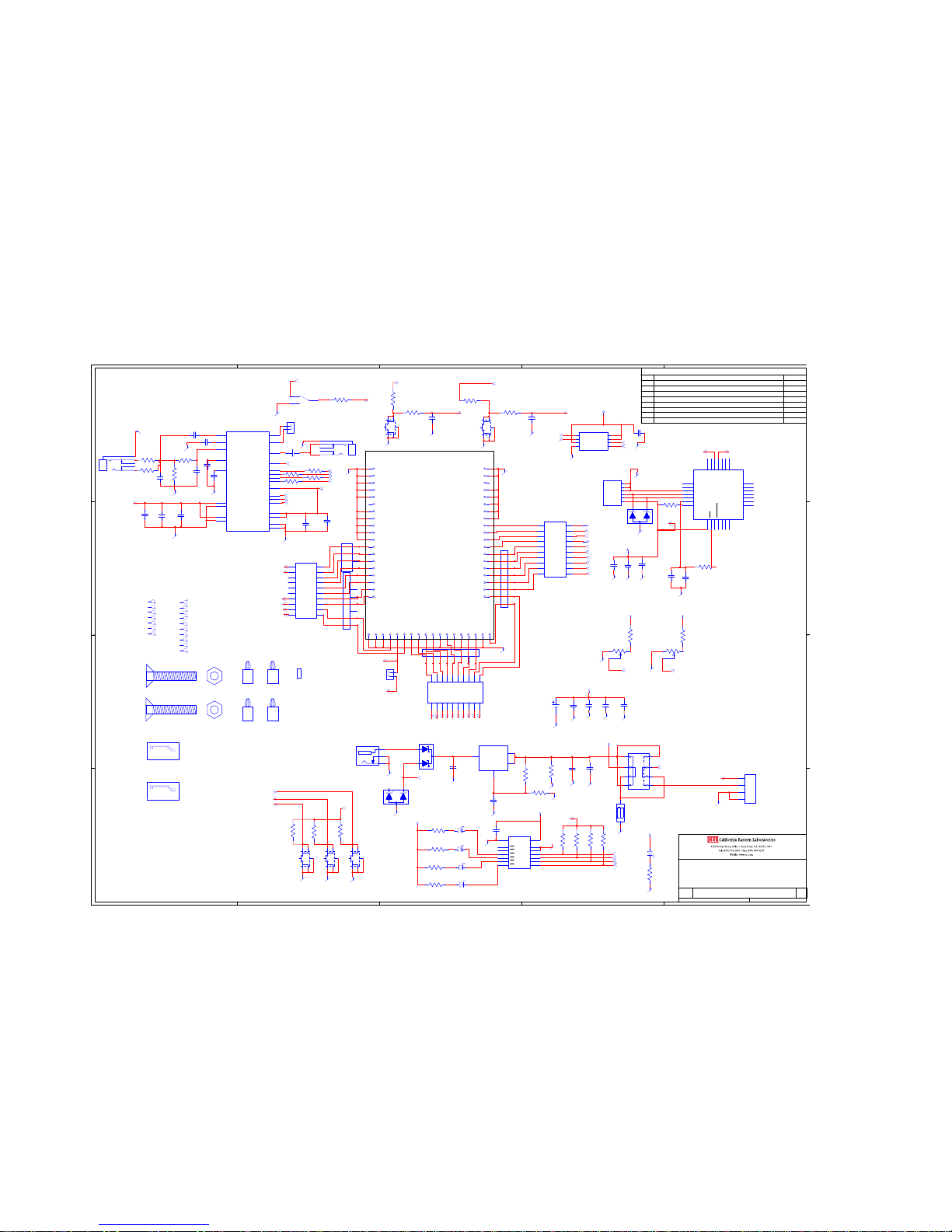
APPENDIX-1: SCHEMATIC OF ZICM2410-EVB3
(CEL Doc # 0007-01-01-03-001 Issue ES3-X2)
Figure 9 – Diagram, ZICM2410-EVB3 Schematic
ES3-X2
ZICM2410 EVAL BD ASSEMBLY SCHEMATIC
C
Sept 6, 2008
ISSUE
Drawing Title:
Size Document Number
Date: Sheet of11
Push
Buttons
LEDs
Reset
Button
Power ON
ZIC 2410 Module Land
SENSE+
SENSE-
B
C
D
5 4 3 2 1
D
C
B
A
2345
0007-01-01-03-001
SPI FLASH
09/06/08
REVISION RECORD
DESCRIPTION: DATE:
ISSUE
PRELIMINARY
ES
ES1
REVISED PER ECR#000022 11/12/08
TX ENABLE
RX ENABLE
Audio Codec
Headphone Jack
Microphone Jack
INT0 / Switch 3
INT1 / Switch 4
ACH_2
ACH_3
P17
P16
V = 3.0V nominal
1: VCC, VCC_MODULE = VREG
2: VCC, VCC_MODULE = VBAT
3: VCC = VREG, VCC_MODULE = J4
ES2
ES3-X0
ES3-X1
REVISED PER SPREADSHEET
03/23/09
REVISED PER ECR#000027 12/10/08
01/14/09
ES3-X2
04/03/09
REVISED PER SPREADSHEET
REVISED PER ECR#000036
1
MH2
R6
390
D1
LNJ026
PCB1
0007-01-04-03-001
PCB
1
MH3
1
MH1
D5
POWER
LNJ214
TP138
C52
10nF
GND_4
GND_3
GND_13
GND_17
GND_5
P3_7
GND_MS1
P3_5
P3_4
ACH0
ACH1
ACH2
ACH3
GND_0
GND_MS0
NC2
GND_20
GND_12
P1_7
P1_6
P1_4
P1_3
GND_9
GND_8
GND_7
P1_1
VCC_3V
P1_0
P3_6
GND_10
P3_3
P3_2
GND_11
P3_1
P3_0
GND_6
P0_7
P0_6
P0_5
P0_4
P0_3
P0_2
P0_1
P0_0
DVDD_1_5
ISP
RESET
AVDD_1_5
GND_14
GND_15
GND_16
GND_18
GND_19
NC1
GND_1
CW
1
2
3
VR1/SPKR-VOL
D2
LNJ414
D3
LNJ326
D4
LNJ926
R7
390
R8
390
R9
390
1
MH4
GND_2
D11
D13
1
2
3
J7
+
-
BC2
2462
C9
47uF
6.3WVDC
C12
10nF
1
2
J9
HDR_2X1
C8
4.7uF
SW1
B3S-1100P
SW2
B3S-1100P
SW5
B3S-1100P
1
2
3
4
J3
1
2
3
4
J4
1
2
3
4
5
6
7
8
J5
22-10-2081
1
MH5
1
MH6
1
2
3
4
5
6
7
8
J11
22-10-2081
1234567
8
J14
22-10-2081
1
2
3
SW7
SW/SPDT
APEM
SLB12814
R1
33
C1
NP
C2
NP
1
MH7
1
MH8
1
MH9
1
MH10
1
MH11
1
MH12
1
MH13
1
MH14
1
MH15
1
MH16
1
MH17
SW3
B3S-1100P
SW4
B3S-1100P
DVDD_1R5
AVDD_1R5
R5
33
R15
33
CW
1
2
3
VR2/MIC-VOL
1
DCD
2
RI
3
GND
4
D+
5
D-
6
VDD
7
REGIN
8
VBUS9RST
10NC11
SUSPEND12SUSPEND13NC14NC
15
NC
16
NC
17
NC
18
NC
19
NC
20
NC
21
NC
22NC23
CTS24RTS
25
RXD
26
TXD
27
DSR
28
DTR
U10
CP2102
C25
.1uF
1
/CS
2
SO
3
/WP
4
GND5SI
6
SCK
7
/HOLD
8
VCC
U8
AT25FS010N
JMP1
929955-06
JMP
SCREW1
4-40 X 5/16"
SCREW2
4-40 X 5/16"
NUT1
4-40 NUT
NUT2
4-40 NUT
STANDOFF1
27FSTP00500
STANDOFF2
27FSTP00500
STANDOFF3
27FSTP00500
STANDOFF4
27FSTP00500
1
MICBIAS
2
AVDD
3
AGND
4
DCVDD
5
DBVDD
6
DGND
7
ADCDAT
8
DACDAT
9
FRAME
10
BCLK
11
MCLK
12
CSB/GPIO
13
SCLK
14
SDIN
15
MODE
16
MONOOUT
17
SPKOUTP
18
SPKGND
19
SPKOUTN
20
SPKVDD
21
AUX
22
VMID
23
MICN
24
MICP
25
GND_BOTTOM
U200
WM8974/QFN24
1
2
J200
HDR_2X1
C6
1uF
C11
1uF
C16
1uF
R14
2.2K
R20
NP
C17
NP
SW9
1
3
11
10
2
SW11
R23
0 OHM
R24
0 OHM
ON
ON
ON
ON
ON
ON
ON
ON
ON
OFF
OFF
OFF
OFF
OFF
OFF
OFF
OFF
OFF
ONOFF
1
2
3
4
5
6
7
8
9
10
11
12
13
14
15
16
17
18
19
20
U203
ON
ON
ON
ON
ON
ON
ON
ON
ON
OFF
OFF
OFF
OFF
OFF
OFF
OFF
OFF
OFF
ONOFF
1
2
3
4
5
6
7
8
9
10 11
12
13
14
15
16
17
18
19
20
U204
ONONONONONONONONON
OFF
OFF
OFF
OFF
OFF
OFF
OFF
OFF
OFF
ONOFF
123456789
10 11
121314151617181920
U205
7
GND14VCC
1
A0
3
A1
5
A2
13
A3
11
A4
9
A5
2
O0
4
O1
6
O2
12
O3
10
O4
8
O5
U4
74LVC04-SO14
R2
10K
R10
10K
R17
10K
R18
10K
C27
4.7uF
C18
4.7uF
C19
4.7uF
C20
4.7uF
C23
4.7uF
C28
4.7uF
+
C30
220µF
C24
.1uF
1
ADJ
2
VOUT1
3
VIN
4
VOUT2
U206
R28
165
R29
121
C33
4.7uF
C32
4.7uF
C29
220pF
1
VUSB
2
DATA-
3
DATA+
4
GND
5
SHIELD1
6
SHIELD2
J1
USB-B
C5
.1uF
C26
.1uF
C40
.1uF
C15
4.7uF
C4
1uF
C22
1uF
C31
1uF
C53
1uF
R19 33
R21
33
R25
33
R26
33
R11
390
R12
10K
R13
10K
R22
10K
R3
10K
R4
10K
R16
10K
R30
680
NP
1
2
3
4
C
1A
2A
4A
CA
3A
SW6
D6
TVS_DUAL_SOT23_300W_5V_ONS
R27
12
DUT1
0007-00-00-00-001
DUT
R31
10K
R32
10K
VCC
RESET
GND
GND
GND
RESET
MS2
ACH_0 ACH_1
GND
VUSB
GND
GND
GND
GND
GND
GND
GND
GND
GND
GND
VCC_MODULE_SENSE
GND
MS2
P33P32
P10
GND
P11
VCC
P34
P37
P36
P35
GND
GND
GND
GND
VCC
VCC
P31
P36
P35
P07
GND
GND
VCC
P00
P01
P02
P03
P04
P05
P10
P11
P13
P14
ACH_1
ACH_0
P36
P37
P35
P34
P33
P32
P31
P30
P07
P06
P13
P14
GND
GND
VCC
P03
P02
P01
P30
GND
GND
GND
GND
GND
P05
P00
P06
P04
GND
GND
GND
VCC_MODULE
VCC_MODULE
VCC_MODULE
VCC_MODULE
GND
VCC_MODULE
VCC_MODULE_SENSE
VCC_MODULE
VUSB
GND
GND
GND
GND
VCC
VCC
VCC_MODULE
GND
VCC
VCC
Page 19
ZICM2410-EVB3 Hardware Reference Guide
Rev C Document No. 0007-05-08-03-001 Page 19 of 19
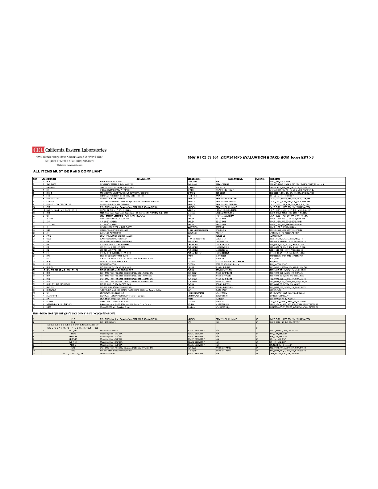
APPENDIX-2: BILL OF MATERIALS (ZICM2410-EVB3)
(CEL Doc # 0007-01-02-03-001 Issue ES-X3) This documen t is subject to revision without notification.
Table 13 – BOM, ZICM2410-EVB3
 Loading...