

CEL UPG2118K User Manual
California Eastern Laboratories
查询UPG2118K供应商
NEC's 1.5W
UPG2118K
GaAs MMIC POWER AMPLIFIER
FEATURES
• E-MODE HJ-FET TECHNOLOGY
• SINGLE +3.2V POWER SUPPLY
• HIGH EFFICIENCY: PAE = 42% MIN
• HIGH SATURATED POWER: Pout = +31.5 dBm MIN
• FLEXIBLE FREQUENCY RANGE
• 20-PIN QFN PACKAGE:
(4.15 X 4.15 X 0.9 mm)
DESCRIPTION
NEC's UPG2118K is a 1.5W, 3 stage power amplifier
developed primarily for DCS/PCS1800 applications.
With modified external matching the UPG2118K can
be tuned from 800 to 2500 MHz.
Use of E-mode FET technology delivers high efficiency
and high linearity with a single positive low voltage
supply.
APPLICATIONS
• 1800 MHz DCS/PCS
• 915 AND 2450 ISM BAND USAGE
• AUTOMATIC METER READERS
• WIRELESS SECURITY
• SATELLITE UPLINK
ORDERING INFORMATION
PART NUMBER MARKING PACKAGE SUPPLYING FORM
UPG2118K-E3 2118 20-pin QFN
• Embossed tape 12mm wide
• 4.5 K pcs/reel
ABSOLUTE MAXIMUM RATINGS (TA = 25°C, unless otherwise specified)
PARAMETERS SYMBOL RATINGS UNIT
Storage Temperature Tstg −45 to +85 °C
Operating Temperature Topt
Supply Voltage1,2,3 VD1,2,3 8.0 V
Active Bias Circuit Voltage V
Reference Voltage V
Junction Temperature Tj 150 °C
Input Power P
Total Power Dissipation P
Caution This device is ESD sensitive. Please take ESD precautions.
The information contained in this document is being issued in advance of the production cycle for the device.
The parameters for the device may change before final production or NEC Corporation, at its own discretion,
may withdraw the device prior to its production.
ABC
ref
in
tot
−45 to +85
8.0 V
5.0 V
15 dBm
4.0 W
°C
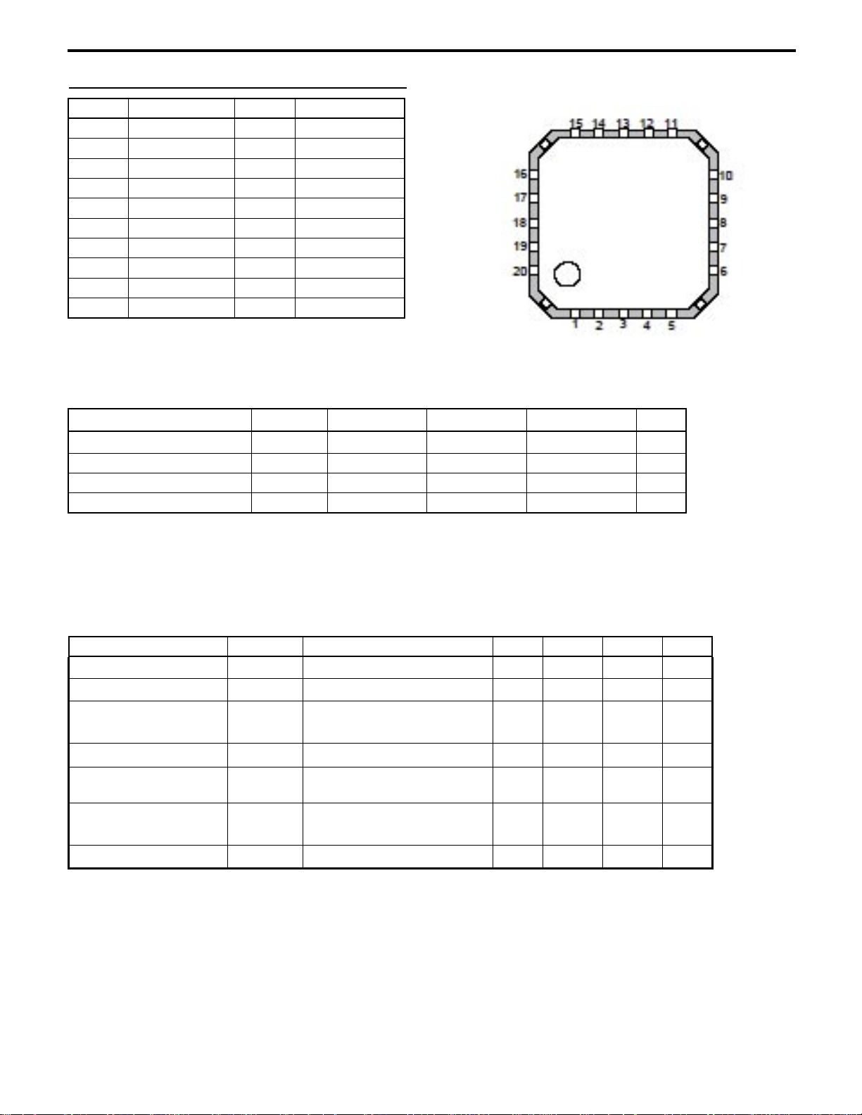
PIN CONNECTIONS
(Top View)
PIN NO. CONNECTION PIN NO. CONNECTION
1 VG1,2 11 GND
2 V
3 V
4 V
5 VG3 15 VD2
6 GND
7 VD3/RF OUT 17 GND
8 VD3/RF OUT 18 GND
9 VD3/RF OUT 19 V
10 VD3/RF OUT 20 RF IN
1,2 12 NC
ref
ABC
3 14 GND
ref
13 NC
16 VD1
attn
RECOMMENDED OPERATING CONDITIONS (TA = 25°C)
PARAMETERS SYMBOL MIN TYP MAX UNIT
Supply Voltage VD1,2,3 +2.8 +3.2 +5.5 V
Reference Voltage V
Active Bias Circuit Voltage V
Input Power P
ref
ABC
in
+0.04 - +1.8 V
0 2.6 5.5 V
5 - 10 dBm
UPG2118K
ELECTRICAL CHARACTERISTICS
(Unless otherwise specified, TA=+25°C,f=1880MHz,VD=+3.2V,V
CHARACTERISTICS SYMBOL TEST CONDITIONS MIN TYP MAX UNIT
Active Bias Circuit Current I
Reference Current I
RF Leakage Current I
Output Power P
ABC
ref
leak
out
Power Added Efficiency PAE 42.0 - - %
Power Control Slope P
Minimum Output Power M
slope
Pout
P
=+31.5dBm,V
out
V
V
V
V
ΔV
V
=0.04 to 1.8V - - 10 mA
ref=Vattn
=0.04 V
ref=Vattn
=10K ohm+Load
ABC
=0.04 V to 1.8V
ref=Vattn
=0.01V
ref
=0.04 V - - -20 dBc
ref=Vattn
ABC
=+2.6V,V
ABC
=1.8V, Pin=+5dBm)
ref=Vattn
=Arbitrary - - 30 mA
- - 50 mA
+31.5 - - dBm
- - 50:1
Vrms/
Vref
 Loading...