

y
查询PS710E-1A供应商
Solid State Rela
PS710E-1A,PS710EL-1A
6-PIN DIP, 0.08 Ω LOW ON-STATE RESISTANCE
2.0 A CONTINUOUS LOAD CURRENT
1-ch Optical Coupled MOS FET
DESCRIPTION
The PS710E-1A and PS710EL-1A are solid state relays containing a GaAs LED on the input side and MOS FETs
on the output side.
It is suitable for PLC, etc. because of its large continuous load current and low on-state resistance.
The PS710EL-1A has a surface mount type lead.
FEATURES
• Low on-state resistance (Ron = 0.08 Ω TYP.)
• Large continuous load current (I
• 1 channel type (1 a output)
• Low LED operating current (I
• Designed for AC/DC switching line changer
• Small package (6-pin DIP)
• Low offset voltage
• PS710EL-1A: Surface mount type
APPLICATIONS
• Measurement equipment
• FA equipment
L = 2.0 A)
F = 2 mA)
−NEPOC Series−
OCMOS FET
Document No. PN10127EJ01V0DS (1st edition)
Date Published April 2002 CP(K)
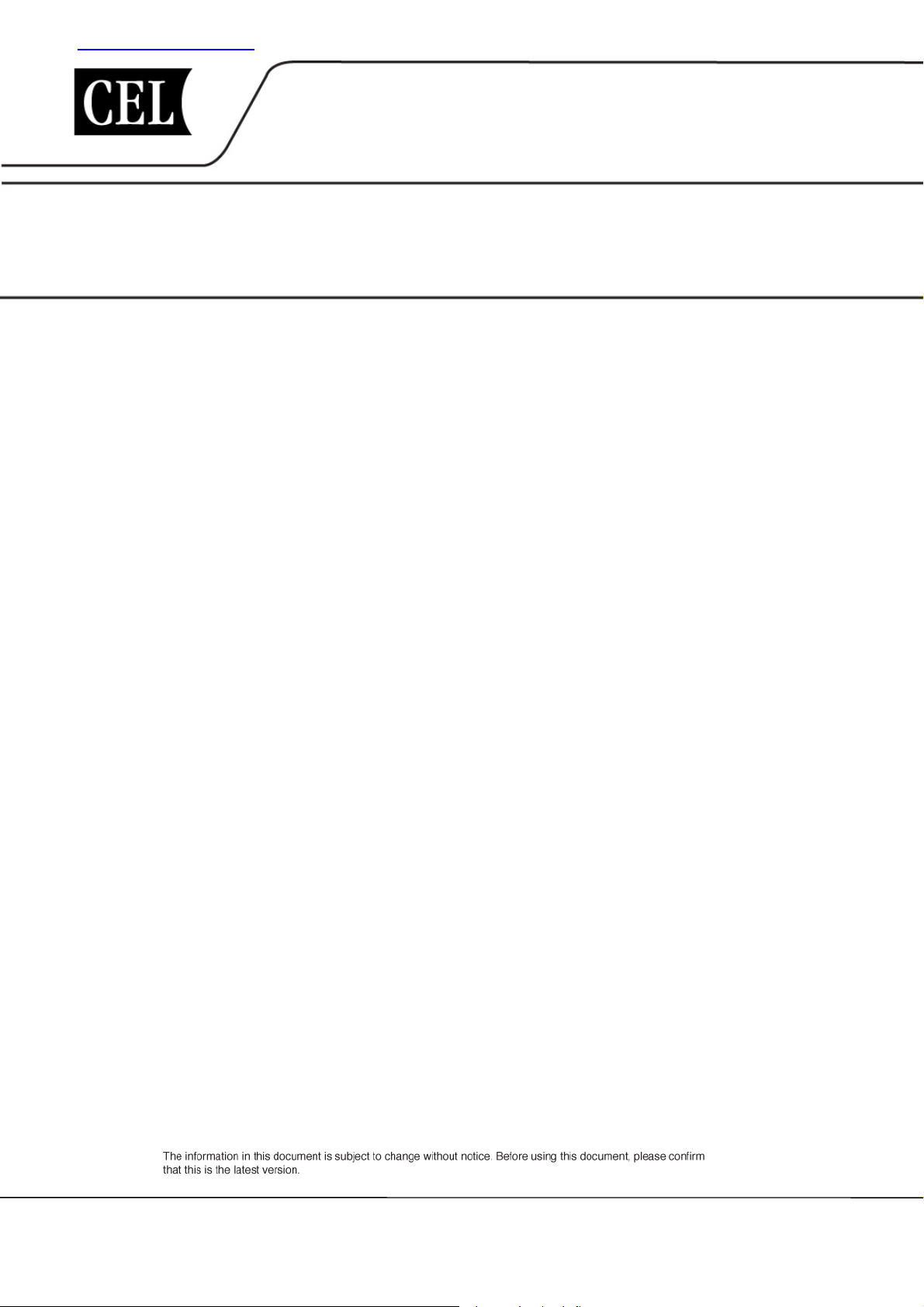
PACKAGE DIMENSIONS (UNIT: mm)
PS710E-1A,PS710EL-1A
PS710E-1A
4.15±0.3
3.3±0.3
0.5±0.1
1.34±0.1
0.25 M
±0.3
3.5
9.25±0.5
2.54
PS710EL-1A
TOP VIEW
654
123
7.62
6.5±0.5
0 to 15˚
1. LED Anode
2. LED Cathode
3. NC
4. MOS FET Drain
5. MOS FET Source
6. MOS FET Drain
±0.3
3.5
1.34±0.1
0.25 M
9.25±0.5
654
123
2.54
TOP VIEW
6.5±0.5
0.9±0.25
9.60±0.4
1. LED Anode
2. LED Cathode
3. NC
4. MOS FET Drain
5. MOS FET Source
6. MOS FET Drain
+0.10
–0.05
0.10
2
Data Sheet PN10127EJ01V0DS
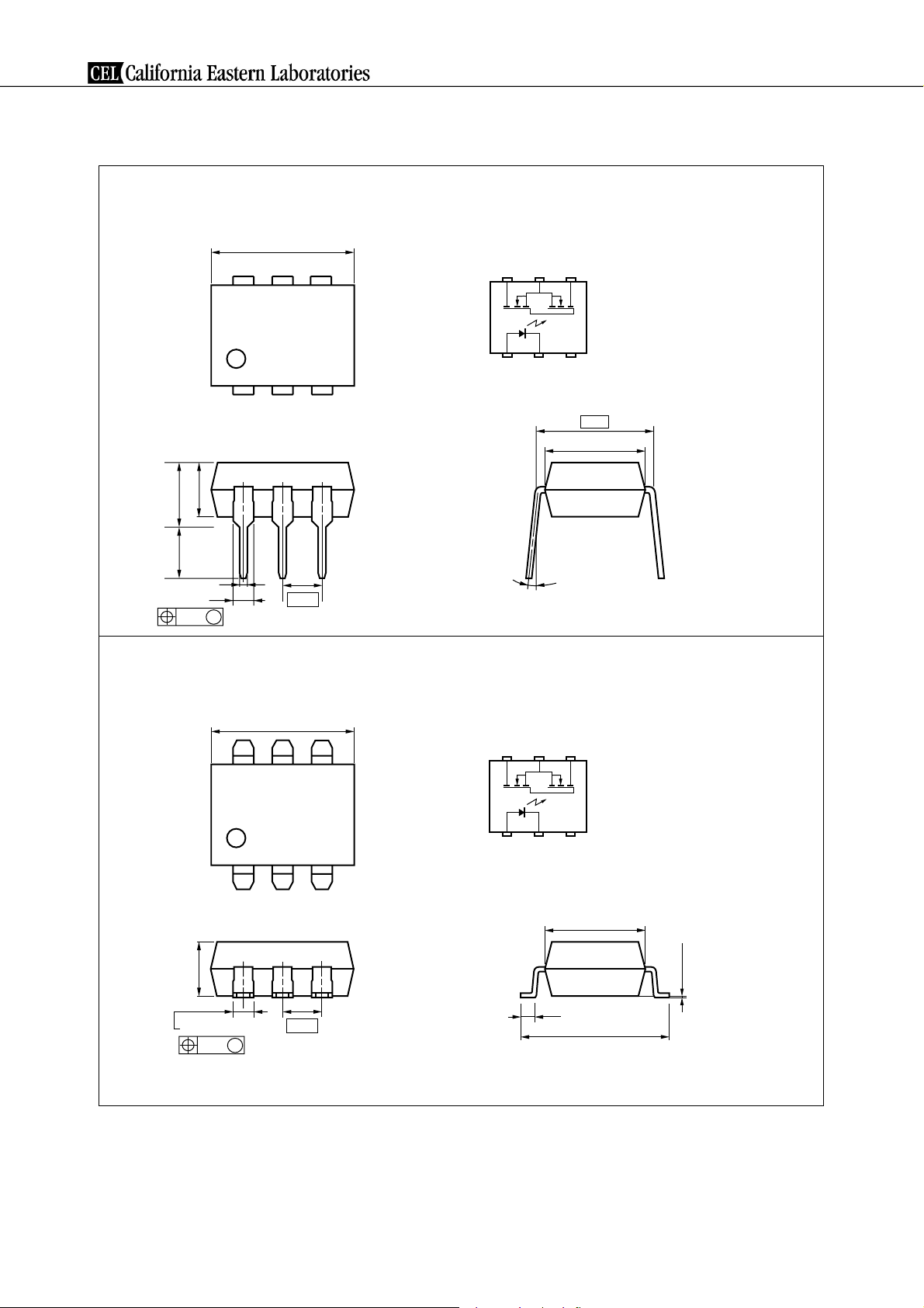
MARKING EXAMPLE
PS710E-1A,PS710EL-1A
No. 1 pin
Mark
PS710E-1A
NE000
0
N
Rank Code
Nothing
00
Year Assembled
(Last 1 Digit)
In-house Code
Solder dipping
Solder plating
E
Country Assembled
Type Number
Assembly Lot
Week Assembled
Data Sheet PN10127EJ01V0DS
3
PS710E-1A,PS710EL-1A
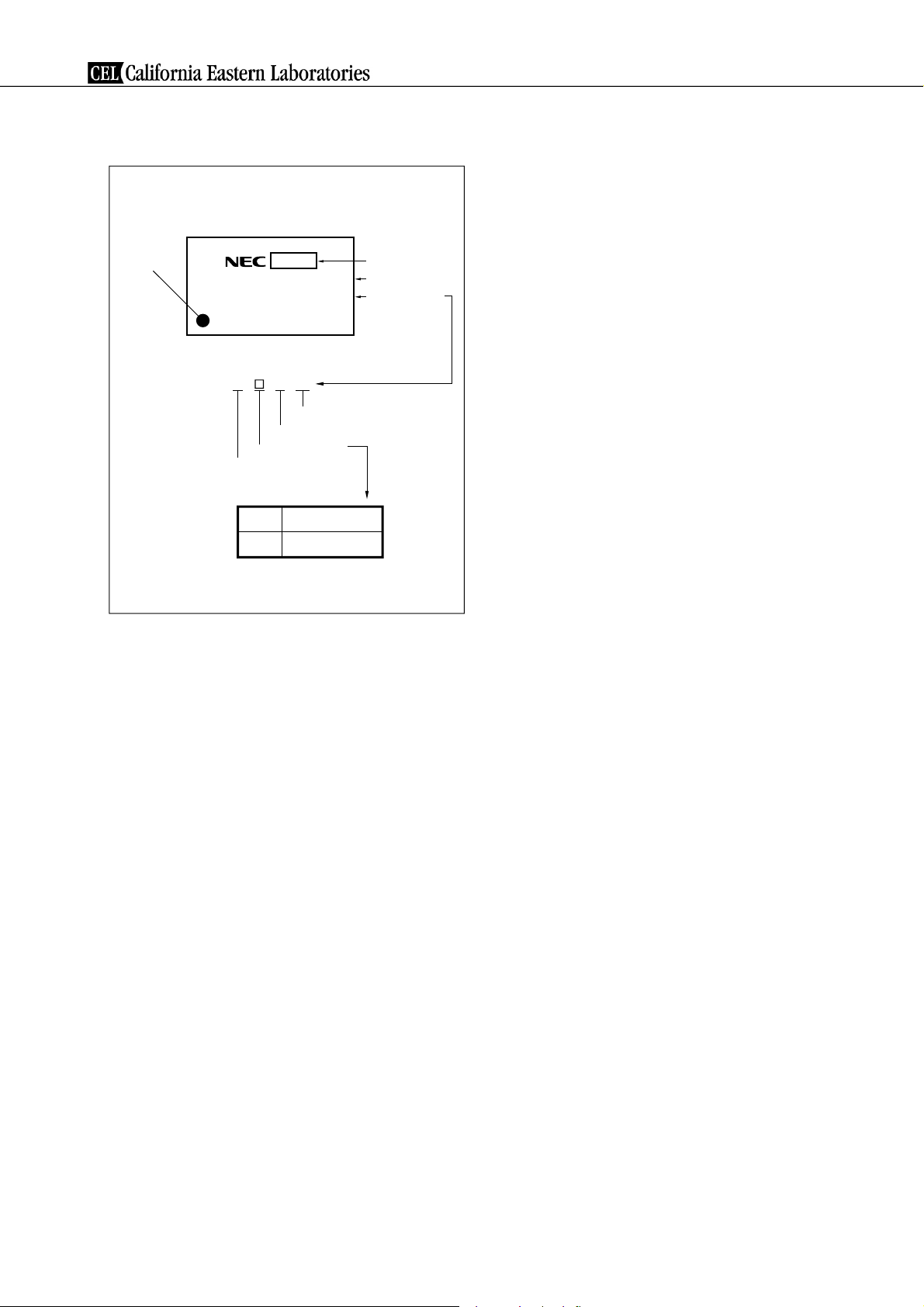
ORDERING INFORMATION (Solder Contains Lead)
Part Number Package Packing Style Application Part Number
PS710E-1A 6-pin DIP Magazine case 50 pcs PS710E-1A
PS710EL-1A PS710EL-1A
PS710EL-1A-E3 Embossed tape 1 000 pcs/reel
PS710EL-1A-E4
*1 For the application of the Safety Standard, following part number should be used.
ORDERING INFORMATION (Pb-Free)
Part Number Package Packing Style Application Part Number
PS710E-1A-A 6-pin DIP Magazine case 50 pcs PS710E-1A
PS710EL-1A-A PS710EL-1A
PS710EL-1A-E3-A Embossed tape 1 000 pcs/reel
PS710EL-1A-E4-A
*1 For the application of the Safety Standard, following part number should be used.
*1
*1
4
Data Sheet PN10127EJ01V0DS

PS710E-1A,PS710EL-1A
ABSOLUTE MAXIMUM RATINGS (TA = 25°C, unless otherwise specified)
Parameter Symbol Ratings Unit
Diode Forward Current (DC) IF 50 mA
Reverse Voltage VR 5.0 V
Power Dissipation PD 50 mW
Peak Forward Current
MOS FET Load Voltage VL 80 V
Continuous Connection A IL 2.0 A
Load Current
*2
Connection C 4.0
Pulse Load Current*3
(AC/DC Connection)
Power Dissipation PD 600 mW
Isolation Voltage
*4
Total Power Dissipation PT 650 mW
Operating Ambient Temperature TA −40 to +85 °C
Storage Temperature Tstg −40 to +100 °C
µ
*1 PW = 100
*2 Conditions: I
s, Duty Cycle = 1%
F ≥ 2 mA. The following types of load connections are available.
*3 PW = 100 ms, 1 shot
*4 AC voltage for 1 minute at T
*1
IFP 1 A
Connection B 3.0
ILP 4.0 A
BV 1 500 Vr.m.s.
Connection A VL (AC/DC)
25
3
1
2
1
Connection B
1
2
3
1
Connection C
2
3
A = 25°C, RH = 60% between input and output
6
I
L
4
6
5
L
L
I
L
+
V
L
(DC)
–
43
6
5
I
L
4
6
5
4
L
I
L
L
IL + I
I
L
L
–
V
L
(DC)
+
+
V
L
(DC)
–
Data Sheet PN10127EJ01V0DS
5

PS710E-1A,PS710EL-1A
RECOMMENDED OPERATING CONDITIONS (TA = 25°C)
Parameter Symbol MIN. TYP. MAX. Unit
LED Operating Current IF 2 10 20 mA
LED Off Voltage VF 0 0.5 V
ELECTRICAL CHARACTERISTICS (TA = 25°C)
Parameter Symbol Conditions MIN. TYP. MAX. Unit
Diode Forward Voltage VF IF = 10 mA 1.2 1.4 V
Reverse Current IR VR = 5 V 5.0
MOS FET Off-state Leakage
Current
Output Capacitance Cout VD = 0 V, f = 1 MHz 480 pF
Coupled LED On-state Current IFon IL = 2.0 A 2.0 mA
On-state Resistance Ron IF = 10 mA, IL = 2.0 A, t ≤ 10 ms 0.083 0.15
Turn-on Time
Turn-off Time
*1, 2
*1, 2
Isolation Resistance RI-O VI-O = 1.0 kVDC 10
Isolation Capacitance CI-O V = 0 V, f = 1 MHz 0.5 pF
*1 Test Circuit for Switching Time
I
F
Pulse Input
ILoff VD = 80 V 50 nA
ton IF = 10 mA, VO = 5 V, RL = 500 Ω, 1.0 2.0 ms
toff PW ≥ 10 ms 0.02 0.2
9
V
L
Input
50%
µ
A
Ω
Ω
0
Input monitor monitorV
O
VO = 5 V
90%
Output
R
in
R
L
t
on
t
off
10%
*2 The turn-on time and turn-off time are specified as input-pulse width ≥ 10 ms.
Be aware that when the device operates with an input-pulse width of under 10 ms, the turn-on time and turn-off
time will increase.
6
Data Sheet PN10127EJ01V0DS

PS710E-1A,PS710EL-1A
TYPICAL CHARACTERISTICS (TA = 25°C, unless otherwise specified)
MAXIMUM FORWARD CURRENT vs.
AMBIENT TEMPERATURE
100
MAXIMUM LOAD CURRENT vs.
AMBIENT TEMPERATURE
3.0
80
60
40
20
Maximum Forward Current IF (mA)
1.6
1.4
1.2
1.0
Forward Voltage VF (V)
2.5
2.0
50
1.5
1.0
0.5
Maximum Load Current IL (A)
0
Ambient Temperature TA (˚C)
FORWARD VOLTAGE vs.
AMBIENT TEMPERATURE
85
7550250–25
100
0.0
7550250–25
Ambient Temperature TA (˚C)
OUTPUT CAPACITANCE vs.
APPLIED VOLTAGE
85
100
600
IF = 50 mA
30 mA
500
f = 1 MHz
20 mA
10 mA
5 mA
400
1 mA
300
200
100
Output Capacitance Cout (pF)
0.8
Ambient Temperature TA (˚C)
OFF-STATE LEAKAGE CURRENT vs.
AMBIENT TEMPERATURE
–6
10
VD = 80 V
–7
10
–8
10
–9
10
–10
10
Off-state Leakage Current ILoff (A)
–11
10
0 20 40 60 80 100
Ambient Temperature TA (˚C)
7550250–25
100
Data Sheet PN10127EJ01V0DS
0
2010
30 40
Applied Voltage VD (V)
LOAD CURRENT vs. LOAD VOLTAGE
3.0
2.0
1.0
–0.2 –0.1 0.1 0.2
–0.3 0 0.3
–1.0
Load Current IL (A)
–2.0
–3.0
Load Voltage VL (V)
IF = 10 mA
7
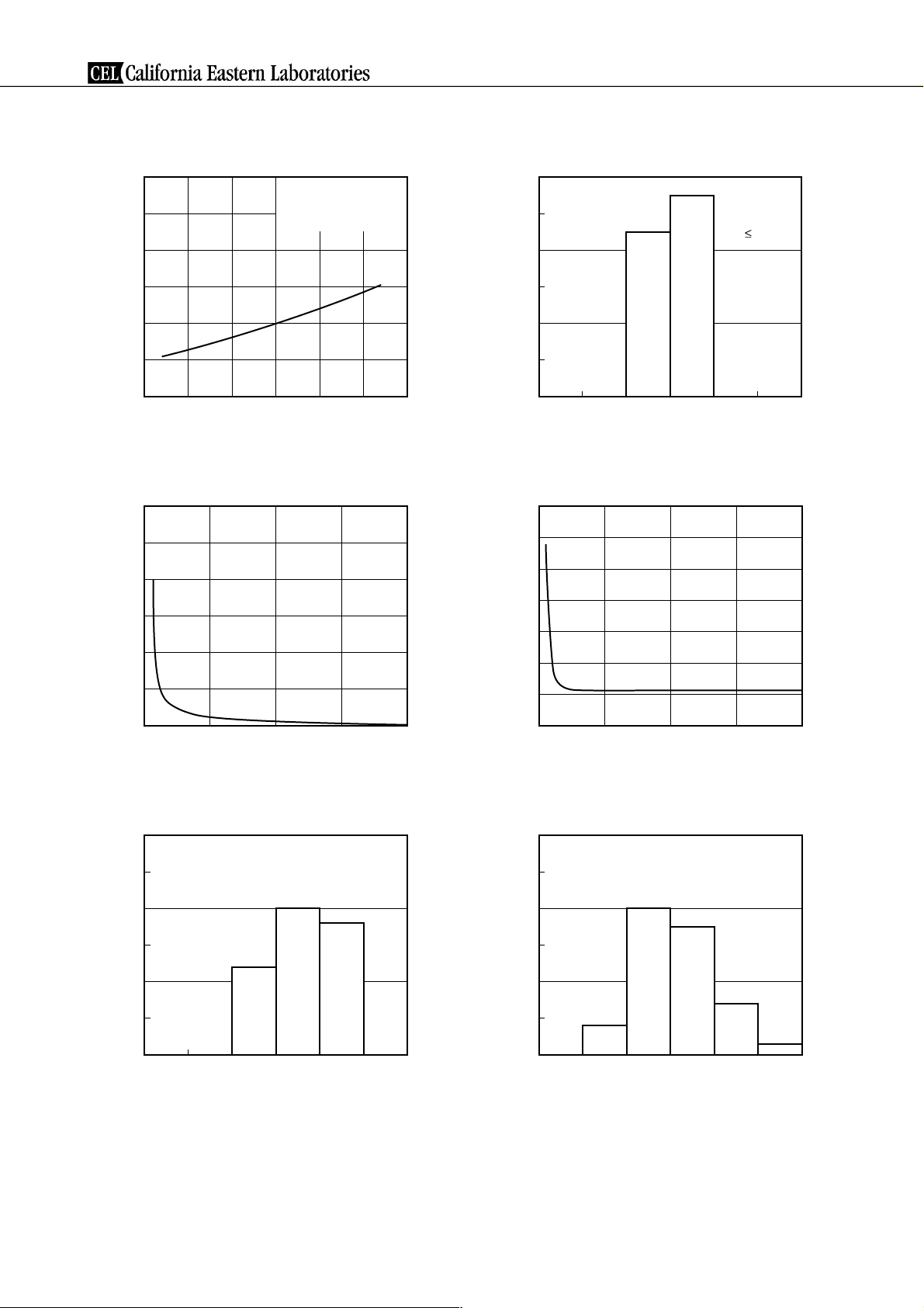
NORMALIZED ON-STATE RESISTANCE vs.
AMBIENT TEMPERATURE
3.0
on
2.5
2.0
Normalized to 1.0
at TA = 25˚C,
F
= 10 mA, IL = 2.0 A
I
PS710E-1A,PS710EL-1A
ON-STATE RESISTANCE DISTRIBUTION
30
25
20
n = 50 pcs,
I
F
= 10 mA,
L
= 2.0 A,
I
t 10 ms
1.5
1.0
0.5
Normalized On-state Resistance R
0.0
–25
25
0–50
Ambient Temperature T
A
(˚C)
7550
TURN-ON TIME vs. FORWARD CURRENT
15
(ms)
10
on
5
Turn-on Time t
0
2010
Forward Current IF (mA)
VO = 5 V,
L
= 500 Ω
R
30
100
40
15
Number (pcs)
10
5
0
7876
82 8480
On-state Resistance Ron (mΩ)
TURN-OFF TIME vs. FORWARD CURRENT
0.14
0.12
0.10
(ms)
off
0.08
0.06
0.04
Turn-off Time t
0.02
0
10
20
Forward Current IF (mA)
VO = 5 V,
L
= 500 Ω
R
30
40
30
25
20
15
Number (pcs)
10
5
0
8
TURN-ON TIME DISTRIBUTION
n = 50 pcs,
I
F
= 10 mA,
O
= 5 V,
V
L
= 500 Ω
R
0.6 0.70.5
Turn-on Time t
0.8 0.9
on
(ms)
30
25
20
15
Number (pcs)
10
5
0
Data Sheet PN10127EJ01V0DS
TURN-OFF TIME DISTRIBUTION
n = 50 pcs,
I
F
= 10 mA,
O
= 5 V,
V
L
= 500 Ω
R
0.0180.0160.014 0.0200.012
Turn-off Time t
off
(ms)

PS710E-1A,PS710EL-1A
NORMALIZED TURN-ON TIME vs.
AMBIENT TEMPERATURE
3.0
Normalized to 1.0
on
2.5
2.0
1.5
1.0
0.5
Normalized Turn-on Time t
0.0
–25
0–50
Ambient Temperature TA (˚C)
Remark The graphs indicate nominal characteristics.
at TA = 25˚C,
I
F
= 10 mA, VO = 5 V,
RL = 500 Ω
25
100
7550
NORMALIZED TURN-OFF TIME vs.
AMBIENT TEMPERATURE
3.0
off
2.5
2.0
1.5
1.0
0.5
Normalized Turn-off Time t
0.0
–25
0–50
Ambient Temperature TA (˚C)
Normalized to 1.0
at T
A
I
F
= 10 mA, VO = 5 V,
L
= 500 Ω
R
25
= 25˚C,
100
7550
Data Sheet PN10127EJ01V0DS
9
TAPING SPECIFICATIONS (UNIT: mm)
Outline and Dimensions (Tape)
PS710E-1A,PS710EL-1A
2.0±0.1
4.0±0.1
1.55±0.1
Tape Direction
PS710EL-1A-E3 PS710EL-1A-E4
12.0±0.1
1.5
+0.1
–0
10.4±0.1
1.75±0.1
7.5±0.1
16.0±0.3
4.5 MAX.
10.3±0.1
4.0±0.1
0.3
Outline and Dimensions (Reel)
R 1.0
Packing: 1 000 pcs/reel
2.0±0.5
13.0±0.2
φ
21.0±0.8
φ
330±2.0
100±1.0
φ
φ
2.0±0.5
17.5±1.0
21.5±1.0
15.9 to 19.4
Outer edge of
flange
10
Data Sheet PN10127EJ01V0DS

PS710E-1A,PS710EL-1A
RECOMMENDED SOLDERING CONDITIONS
(1) Infrared reflow soldering
• Peak reflow temperature 260°C or below (package surface temperature)
• Time of peak reflow temperature 10 seconds or less
• Time of temperature higher than 220°C 60 seconds or less
• Time to preheat temperature from 120 to 180°C 120±30 s
• Number of reflows Three
• Flux Rosin flux containing small amount of chlorine (The flux with a
maximum chlorine content of 0.2 Wt% is recommended.)
Recommended Temperature Profile of Infrared Reflow
(heating)
to 10 s
260˚C MAX.
220˚C
to 60 s
180˚C
120˚C
Package Surface Temperature T (˚C)
120±30 s
(preheating)
Time (s)
(2) Wave soldering
• Temperature 260°C or below (molten solder temperature)
• Time 10 seconds or less
• Preheating conditions 120°C or below (package surface temperature)
• Number of times One
• Flux Rosin flux containing small amount of chlorine (The flux with a maximum chlorine
content of 0.2 Wt% is recommended.)
(3) Cautions
• Fluxes
Avoid removing the residual flux with freon-based and chlorine-based cleaning solvent.
Data Sheet PN10127EJ01V0DS
11
4590 Patrick Henry Drive
Santa Clara, CA 95054-1817
Telephone: (408) 919-2500
Facsimile:
(
408) 988-0279
Subject: Compliance with EU Directives
CEL certifies, to its knowledge, that semiconductor and laser products detailed below are compliant
with the requirements of European Union (EU) Directive 2002/95/EC Restriction on Use of Hazardous
Substances in electrical and electronic equipment (RoHS) and the requirements of EU Directive
2003/11/EC Restriction on Penta and Octa BDE.
CEL Pb-free products have the same base part number with a suffix added. The suffix –A indicates
that the device is Pb-free. The –AZ suffix is used to designate devices containing Pb which are
exempted from the requirement of RoHS directive (*). In all cases the devices have Pb-free terminals.
All devices with these suffixes meet the requirements of the RoHS directive.
This status is based on CEL’s understanding of the EU Directives and knowledge of the materials that
go into its products as of the date of disclosure of this information.
Restricted Substance
per RoHS
Concentration Limit per RoHS
(values are not yet fixed)
Concentration contained
in CEL devices
-A -AZ
Lead (Pb) < 1000 PPM
Not Detected (*)
Mercury < 1000 PPM Not Detected
Cadmium < 100 PPM Not Detected
Hexavalent Chromium < 1000 PPM Not Detected
PBB < 1000 PPM Not Detected
PBDE < 1000 PPM Not Detected
If you should have any additional questions regarding our devices and compliance to environmental
standards, please do not hesitate to contact your local representative.
Important Information and Disclaimer: Information provided by CEL on its website or in other communications concerting the substance
content of its products represents knowledge and belief as of the date that it is provided. CEL bases its knowledge and belief on information
provided by third parties and makes no representation or warranty as to the accuracy of such information. Efforts are underway to better
integrate information from third parties. CEL has taken and continues to take reasonable steps to provide representative and accurate
information but may not have conducted destructive testing or chemical analysis on incoming materials and chemicals. CEL and CEL
suppliers consider certain information to be proprietary, and thus CAS numbers and other limited information may not be available for
release.
In no event shall CEL’s liability arising out of such information exceed the total purchase price of the CEL part(s) at issue sold by CEL to
customer on an annual basis.
See CEL Terms and Conditions for additional clarification of warranties and liability.
 Loading...