

查询NE677M04供应商
NEC's MEDIUM POWER
NPN SILICON HIGH FREQUENCY
FEATURES
• HIGH GAIN BANDWIDTH:
T = 15 GHz
f
• HIGH OUTPUT POWER:
P-1dB = 15 dBm at 1.8 GHz
• HIGH LINEAR GAIN:
G
L
= 15.5 dB at 1.8 GHz
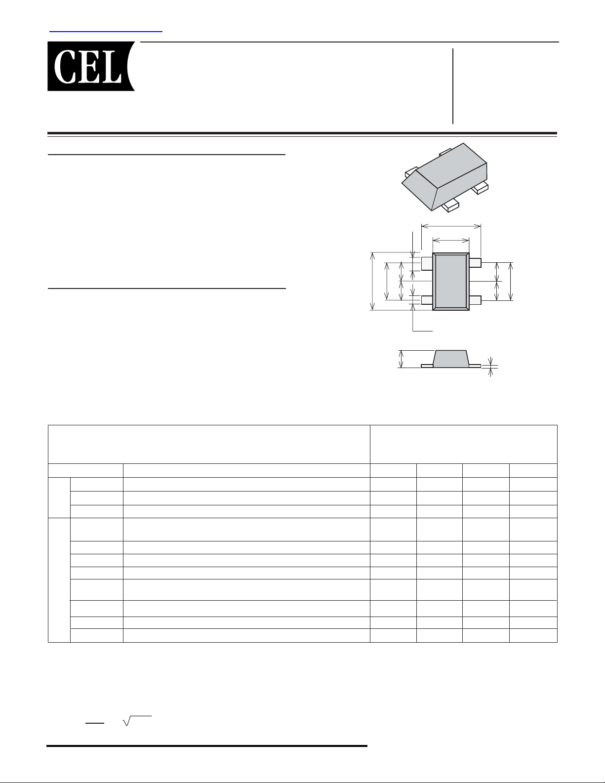
• NEW LOW PROFILE M04 PACKAGE:
SOT-343 footprint, with a height of only 0.59 mm
Flat lead style for better RF performance
DESCRIPTION
NEC's NE677M04 is fabricated using NEC's HFT3 wafer
process. With a transition frequency of 15 GHz, the NE677M04
is usable in applications from 100 MHz to 3 GHz. The NE677M04
provides P1dB of 15 dBm, even with low voltage and low
current, making this device an excellent choice for the driver
stage for mobile or fixed wireless applications.
NEC's NE677M04 is housed in NEC's new low profile/flat lead
style "M04" package
ELECTRICAL CHARACTERISTICS (TA = 25°C)
PART NUMBER NE677M04
PACKAGE OUTLINE M04
EIAJ3 REGISTRATION NUMBER 2SC5751
TRANSISTOR
2.05±0.1
+0.30
-0.05
1.25±0.1
+0.40
2
2.0±0.1
0.65
1.25
0.65
1
+0.30
0.59±0.05
PIN CONNECTIONS
1. Emitter
2. Collector
3. Emitter
4. Base
+0.01
-0.05
NE677M04
R54
3
0.65
0.65
4
(leads 1, 3 and ,4)
1.30
+0.1
+0.11
-0.05
SYMBOLS PARAMETERS AND CONDITIONS UNITS MIN TYP MAX
ICBO Collector Cutoff Current at VCB = 5V, IE = 0 nA 100
IEBO Emitter Cutoff Current at VEB = 1 V, IC = 0 nA 100
DC
hFE DC Current1 Gain at VCE = 3 V, IC = 20 mA 75 120 150
P1dB Output Power at 1 dB compression point at VCE = 2.8 V, ICQ = 8 mA, dBm 15.0
GL Linear Gain at VCE = 2.8 V, ICQ = 8 mA, f = 1.8 GHz, Pin = -10 dBm dB 15.5
MAG Maximum Available Gain4 at VCE = 3 V, IC = 20 mA, f = 2 GHz dBm 16.0
RF
|S21E|
ηc Collector Efficiency at VCE = 2.8 V, ICQ = 8 mA, f = 1.8 GHz, % 50
NF Noise Figure at VCE = 3 V, IC = 5 mA, f = 2 GHz, Zs =ZOPT dB 1.7 2.5
fT Gain Bandwidth at VCE = 3 V, IC = 20 mA, f = 2 GHz GHz 15
Cre Reverse Transfer Capacitance2 at VCB = 3 V, IC = 0, f = 1 MHz pF 0.22 0.50
Notes:
1. Pulsed measurement, pulse width ≤ 350 µs, duty cycle ≤ 2 %.
2. Collector to Base capacitance measured by capacitance meter(automatic balance bridge method) when emitter pin is connected to the
guard pin of capacitance meter.
3. Electronic Industrail Association of Japan
21
|S
MAG =
4.
|S12|
f = 1.8 GHz, Pin = 1 dBm
2
Insertion Power Gain at VCE = 3 V, IC = 20 mA, f = 2 GHz dB 10.0 13.5
Pin = 1 dBm
K ±
2
K - 1
).
|
(
California Eastern Laboratories
NE677M04
ABSOLUTE MAXIMUM RATINGS
1
(TA = 25°C)
SYMBOLS PARAMETERS UNITS RATINGS
VCBO Collector to Base Voltage V 9.0
VCEO Collector to Emitter Voltage V 6.0
EBO Emitter to Base Voltage V 2.0
V
IC Collector Current mA 50
P
T Total Power Dissipation
2
mW 205
TJ Junction Temperature °C 150
STG Storage Temperature °C -65 to +150
T
Note:
1. Operation in excess of any one of these parameters may result
in permanent damage.
2. Mounted on a 1.08cm2 x 1.0 mm thick glass epoxy PCB.
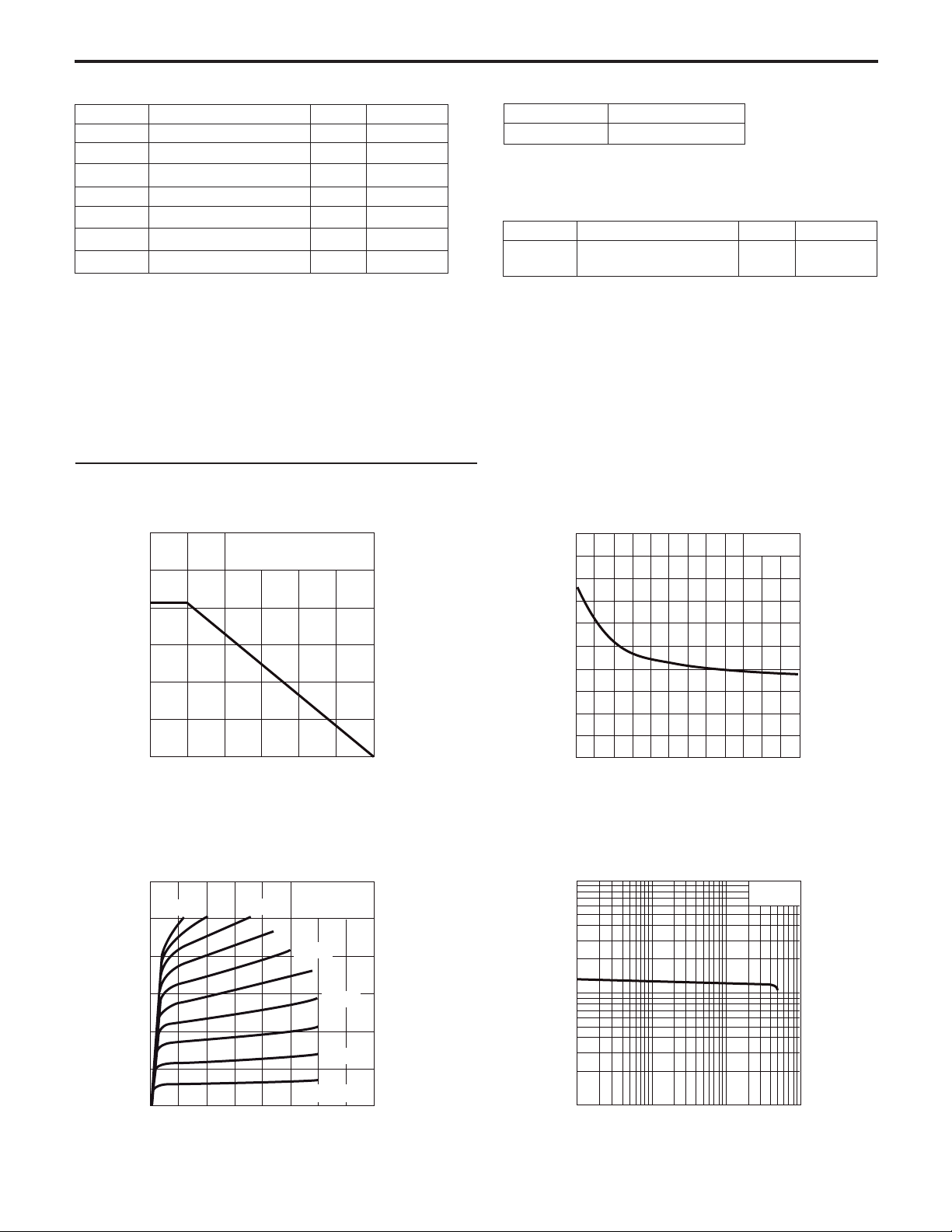
TYPICAL PERFORMANCE CURVES (TA = 25 °C)
TOTAL POWER DISSIPATION
vs. AMBIENT TEMPERATURE
(mW)
out
300
250
200
150
100
Mounted on Glass Epoxy PCB
2
x 1.0 mm (t) )
(1.08 cm
ORDERING INFORMATION
PART NUMBER QUANTITY
NE677M04-T2 3k pcs./reel
THERMAL RESISTANCE
SYMBOLS PARAMETERS UNITS RATINGS
Rth j-a Thermal Resistance from °C/W 600
Note:
1. Mounted on a 1.08cm
(pF)
re
Junction to Ambient
2
x 1.0 mm thick glass epoxy PCB.
REVERSE TRANSFER CAPACITANCE
vs. COLLECTOR TO BASE VOLTAGE
0.5
0.4
0.3
0.2
f = 1MH
z
50
Total Power Dissipation P
0255075100125150
Ambient Temperature TA (ºC)
COLLECTOR CURRENT vs.
COLLECTOR TO EMITTER VOLTAGE
60
400 µA
(mA)
C
500 µA
50
40
30
20
Collector Current I
10
012345678
IB: 50 µA step
300 µA
200 µA
100 µA
IB: 50 µA
500 µA
Collector to Emitter Voltage VCE (V)
0.1
Reverse Transfer Capacitance C
0123456
Collector to Base Voltage VCB (V)
DC CURRENT GAIN
vs. COLLECTOR CURRENT
000
)
FE
100
VCE = 3 V
DC Current Gain (h
010
0.1
1
10
Collector Current IC (mA)
100
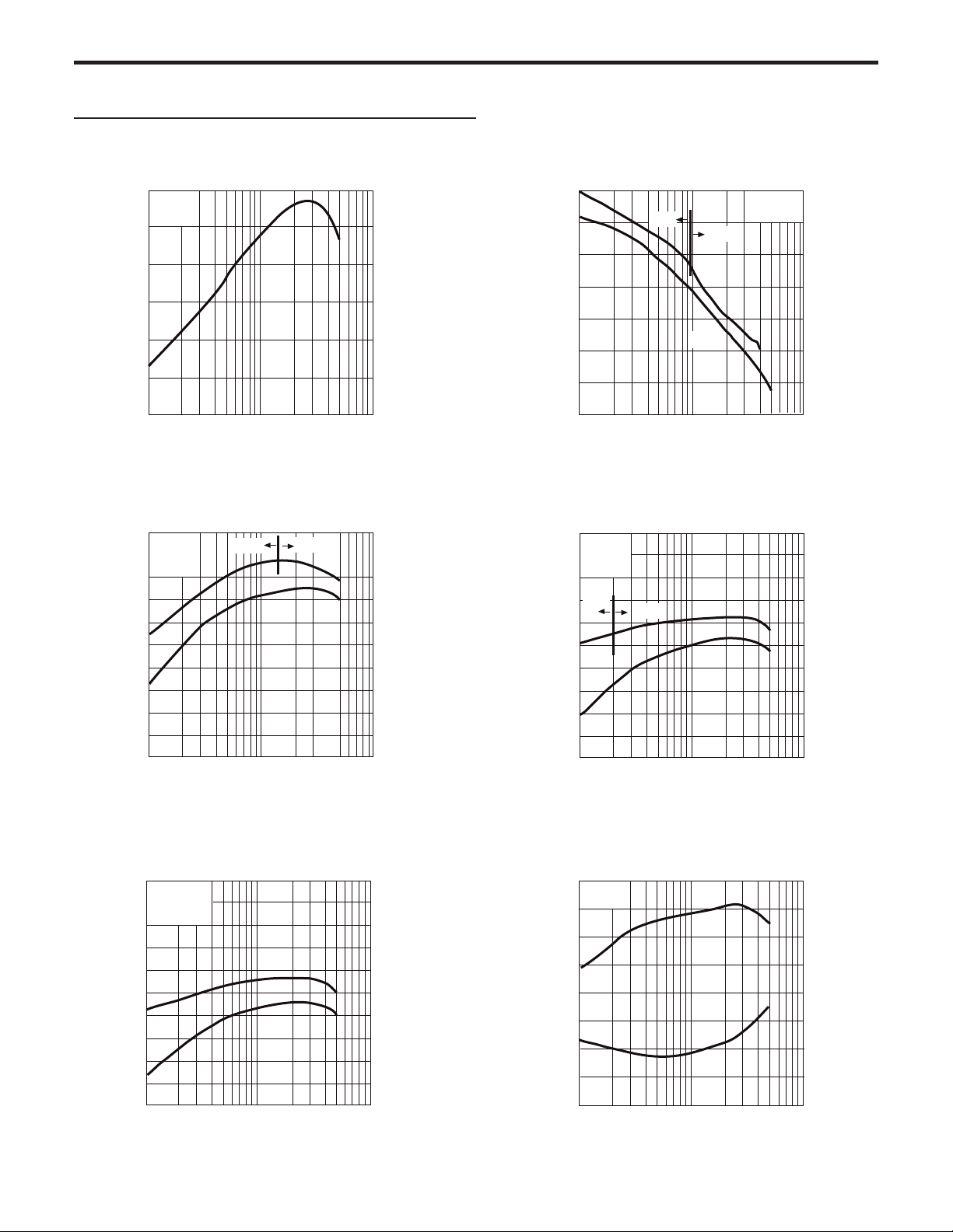
TYPICAL PERFORMANCE CURVES (TA = 25 °C)
NE677M04
GAIN BANDWIDTH PRODUCT
vs. COLLECTOR CURRENT
15
VCE = 3 V
f = 2 GHz
(GHz)
T
10
5
Gain Bandwidth Product f
0
110100
Collector Current IC (mA)
INSERTION POWER GAIN,
MAG, MSG vs. COLLECTOR CURRENT
25
VCE = 3 V
f = 1 GHz
20
, (dB)
2
|
21e
15
MSG
INSERTION POWER GAIN,
MAG, MSG vs. FREQUENCY
, (dB)
2
|
21e
35
MSG
25
MAG
VCE = 3 V
c
= 20 mA
I
20
15
2
|S
21e
10
Insertion Power Gain |S
5
Maximum Stable Power Gain MSG (dB)
0
Maximum Available Power Gain MAG (dB)
0.1 1 10
|
Frequency f (mA)
INSERTION POWER GAIN,
MAG, MSG vs. COLLECTOR CURRENT
, (dB)
|
21e
25
VCE = 3 V
f = 2 GHz
20
MSG
15
MAG
MAG
2
2
21e
|
|S
10
5
Insertion Power Gain |S
Maximum Stable Power Gain MSG (dB)
0
Maximum Available Power Gain MAG (dB)
110100
Collector Current IC (mA)
INSERTION POWER GAIN,
MAG vs. COLLECTOR CURRENT
25
VCE = 3 V
f = 2.5 GHz
20
, (dB)
2
|
21e
15
10
5
MAG
|S
21e
2
|
Insertion Power Gain |S
0
Maximum Available Power Gain MAG (dB)
110100
Collector Current IC (mA)
2
|S
21e
10
5
|
Insertion Power Gain |S
Maximum Stable Power Gain MSG (dB)
0
Maximum Available Power Gain MAG (dB)
110100
Collector Current IC (mA)
NOISE FIGURE, ASSOCIATED GAIN
vs. COLLECTOR CURRENT
8
V
CE
= 3 V
f = 2 GHz
G
a
6
4
Noise Figure NF (dB)
NF
0
110100
Collector Current IC (mA)
16
12
(dB)
a
8
42
Associated Gain G
0

NE677M04
TYPICAL PERFORMANCE CURVES (TA = 25 °C)
OUTPUT POWER, POWER GAIN,
COLLECTOR CURRENT, COLLECTOR
EFFICIENCY vs. INPUT POWER
25
G
P
20
(dbm)
(dB)
p
out
15
10
Power Gain G
Output Power P
5
0
-20 -15 -10 -5 0 5
P
out
V
CE
f = 0.9 GHz
I
cq
= 8 mA (RF OFF)
η
Input Power Pin (dBm)
OUTPUT POWER, POWER GAIN,
COLLECTOR CURRENT, COLLECTOR
EFFICIENCY vs. INPUT POWER
25
20
(dbm)
(dB)
p
out
15
G
P
V
CE
= 3.2 V
f = 1.8 GHz
I
cq
= 8 mA (RF OFF)
= 3.2 V
c
OUTPUT POWER, POWER GAIN,
COLLECTOR CURRENT, COLLECTOR
EFFICIENCY vs. INPUT POWER
250
200
(mA),
C
150
100
Collector Current I
50
I
c
Collector Efficiency ηc (%)
0
25
20
G
(dbm)
(dB)
p
out
P
15
10
Power Gain G
Output Power P
5
0
V
CE
= 2.8 V
f = 1.8 GHz
I
cq
= 8 mA (RF OFF)
P
out
η
c
250
200
(mA),
C
150
100
Collector Current I
50
I
c
0
10-15 -10 -5 0 5
Collector Efficiency ηc (%)
Input Power Pin (dBm)
OUTPUT POWER, POWER GAIN,
COLLECTOR CURRENT, COLLECTOR
EFFICIENCY vs. INPUT POWER
250
200
150
(mA),
C
25
20
(dbm)
(dB)
p
out
15
V
CE
= 3.2 V
f = 2.4 GHz
I
cq
= 8 mA (RF OFF)
G
P
250
200
150
(mA),
C
10
Power Gain G
Output Power P
5
0
P
out
η
c
Input Power Pin (dBm)
100
Collector Current I
50
I
c
0
10-15 -10 -5 0 5
Collector Efficiency ηc (%)
10
Power Gain G
Output Power P
5
0
P
out
η
c
100
Collector Current I
50
I
c
0
10-15 -10 -5 0 5
Collector Efficiency ηc (%)
Input Power Pin (dBm)

TYPICAL SCATTERING PARAMETERS (TA = 25°C)
NE677M04
j10
0
10
S11
j25
25
50
j50
j100
+135º
S22
100
+180º
+90º
10 15 20
5
+45º
+0º+0º
-j10
-45º
-j25
-j50
-135º
-j100
-90º
NE677M04
VC = 2 V, IC = 10 mA
FREQUENCY S11 S21 S12 S22 K MAG
GHz MAG ANG MAG ANG MAG ANG MAG ANG (dB)
0.100 0.72 -28.02 23.85 159.39 0.01 76.80 0.94 -17.17 0.11 32.34
0.200 0.67 -53.32 21.19 142.90 0.02 61.76 0.85 -30.90 0.22 29.46
0.300 0.62 -74.47 18.36 129.52 0.03 53.97 0.75 -41.48 0.30 27.71
0.400 0.57 -91.69 15.78 119.03 0.04 47.84 0.66 -49.21 0.38 26.40
0.500 0.54 -105.42 13.68 110.66 0.04 44.49 0.60 -55.01 0.46 25.44
0.600 0.50 -119.13 11.77 103.58 0.04 41.61 0.51 -57.12 0.62 24.54
0.700 0.48 -128.64 10.42 97.78 0.04 40.18 0.48 -61.53 0.69 23.81
0.800 0.47 -136.17 9.33 92.96 0.05 39.74 0.45 -63.91 0.75 23.13
0.900 0.46 -143.27 8.43 88.43 0.05 39.29 0.43 -66.99 0.82 22.51
1.000 0.46 -148.66 7.70 84.44 0.05 39.40 0.42 -69.40 0.87 21.95
1.500 0.44 -170.56 5.30 67.31 0.06 40.48 0.39 -82.07 1.10 17.66
1.800 0.43 179.75 4.47 58.55 0.06 41.76 0.39 -89.26 1.19 15.82
1.900 0.43 176.51 4.24 55.72 0.07 41.66 0.39 -91.76 1.20 15.33
2.000 0.43 173.63 4.04 52.97 0.07 42.00 0.40 -94.18 1.22 14.87
2.500 0.42 159.00 3.26 39.73 0.08 42.28 0.42 -105.45 1.26 13.00
3.000 0.42 144.48 2.73 27.19 0.10 40.73 0.46 -115.95 1.24 11.64
3.500 0.43 129.44 2.34 15.06 0.11 38.24 0.49 -125.23 1.18 10.67
4.000 0.45 115.14 2.04 3.42 0.13 34.92 0.53 -134.51 1.11 9.99
4.500 0.48 102.37 1.79 -7.89 0.14 30.39 0.56 -144.23 1.04 9.71
5.000 0.50 91.32 1.59 -18.83 0.16 25.33 0.59 -154.88 0.97 9.94
5.500 0.53 81.53 1.42 -29.44 0.18 19.49 0.62 -165.89 0.90 9.00
6.000 0.55 72.28 1.27 -39.61 0.20 13.49 0.66 -176.84 0.85 8.11
1
Note:
1. Gain Calculations:
MAG =
|S
21
|
(
12
|
|S
K –
2
K - 1
MAG = Maximum Available Gain
MSG = Maximum Stable Gain
).
When K ≥ 1, MAG is undefined and MSG values are used.
MSG =
21
|
|S
, K =
|S
12
|
2
1 + | ∆ | - |S
2 |S
12 S21
11
2
| - |S22|
|
2
∆ = S
,
11 S22
- S21 S
12

NE677M04
TYPICAL SCATTERING PARAMETERS (TA = 25°C)
j10
0
10
S11
j25
25
50
j50
100
S22
j100
+135º
+180º
+90º
+45º
10 3020
+0º+0º
-j10
-45º
-j25
-j50
-135º
-j100
-90º
NE677M04
VC = 3 V, IC = 20 mA
FREQUENCY S11 S21 S12 S22 K MAG
GHz MAG ANG MAG ANG MAG ANG MAG ANG (dB)
0.100 0.58 -36.91 34.82 154.30 0.01 65.53 0.91 -19.74 0.28 35.64
0.200 0.53 -67.97 29.03 135.74 0.02 59.98 0.78 -33.77 0.34 32.23
0.300 0.49 -91.49 23.80 122.19 0.02 55.05 0.67 -43.13 0.45 30.35
0.400 0.46 -108.88 19.70 112.29 0.03 51.06 0.58 -49.18 0.56 28.90
0.500 0.44 -121.87 16.66 104.71 0.03 49.50 0.52 -53.43 0.65 27.72
0.600 0.42 -135.00 14.16 98.54 0.03 48.74 0.45 -53.84 0.81 26.72
0.700 0.42 -143.29 12.41 93.35 0.03 49.30 0.42 -57.21 0.89 25.86
0.800 0.41 -149.68 11.03 89.03 0.03 50.12 0.40 -58.72 0.95 25.08
0.900 0.41 -155.84 9.91 84.93 0.04 50.69 0.39 -61.16 0.99 24.32
1.000 0.41 -160.23 9.01 81.35 0.04 51.41 0.38 -63.04 1.04 22.48
1.500 0.40 -178.96 6.14 65.55 0.05 53.28 0.37 -74.89 1.17 18.28
1.800 0.39 172.52 5.16 57.30 0.06 53.31 0.38 -82.12 1.20 16.70
1.900 0.39 169.64 4.90 54.62 0.06 53.31 0.38 -84.61 1.20 16.25
2.000 0.39 167.05 4.66 52.02 0.06 53.16 0.38 -87.15 1.21 15.82
2.500 0.39 153.59 3.75 39.33 0.08 51.37 0.42 -98.84 1.19 14.09
3.000 0.39 139.95 3.14 27.21 0.10 48.43 0.45 -109.77 1.15 12.83
3.500 0.41 125.64 2.68 15.39 0.11 44.68 0.49 -119.46 1.09 12.00
4.000 0.43 111.98 2.34 3.97 0.13 40.02 0.53 -129.07 1.02 11.72
4.500 0.45 99.88 2.06 -7.19 0.15 34.90 0.56 -139.11 0.95 11.48
5.000 0.48 89.38 1.83 -18.07 0.16 29.26 0.60 -150.00 0.88 10.49
5.500 0.51 80.01 1.64 -28.76 0.18 22.90 0.63 -161.27 0.82 9.55
6.000 0.53 71.10 1.47 -39.12 0.20 16.56 0.66 -172.54 0.77 8.69
1
Note:
1. Gain Calculations:
MAG =
|S
21
|
(
12
|
|S
K –
2
K - 1
MAG = Maximum Available Gain
MSG = Maximum Stable Gain
).
When K ≥ 1, MAG is undefined and MSG values are used.
MSG =
21
|
|S
, K =
|S
12
|
2
1 + | ∆ | - |S
2 |S
12 S21
11
2
| - |S22|
|
2
∆ = S
,
11 S22
- S21 S
12

TYPICAL SCATTERING PARAMETERS (TA = 25°C)
NE677M04
j10
0
10
S11
j25
25
50
j50
100
S22
j100
+135º
+180º
+90º
10
20 30 40
+45º
+0º+0º
-j10
-135º
-45º
-90º
NE677M04
VC = 5 V, IC = 30 mA
FREQUENCY S11 S21 S12 S22 K MAG
GHz MAG ANG MAG ANG MAG ANG MAG ANG (dB)
0.100 0.53 -41.03 40.66 151.83 0.01 79.56 0.89 -20.30 0.21 36.62
0.200 0.48 -73.66 32.81 132.70 0.02 64.08 0.75 -33.75 0.39 33.32
0.300 0.44 -97.50 26.31 119.35 0.02 56.29 0.63 -42.07 0.53 31.43
0.400 0.42 -114.52 21.49 109.81 0.02 53.44 0.56 -47.07 0.66 30.03
0.500 0.41 -127.00 18.03 102.57 0.02 53.31 0.50 -50.52 0.75 28.75
0.600 0.39 -139.82 15.28 96.73 0.03 53.08 0.43 -50.09 0.90 27.65
0.700 0.39 -147.57 13.34 91.78 0.03 54.05 0.41 -52.99 0.98 26.75
0.800 0.38 -153.47 11.83 87.64 0.03 55.02 0.40 -54.21 1.02 24.98
0.900 0.38 -159.31 10.62 83.69 0.03 55.65 0.39 -56.48 1.06 23.55
1.000 0.38 -163.26 9.64 80.25 0.04 56.16 0.38 -58.27 1.09 22.49
1.500 0.37 179.14 6.55 64.91 0.05 58.22 0.37 -70.16 1.18 18.69
1.800 0.37 171.01 5.50 56.83 0.06 57.93 0.38 -77.47 1.19 17.16
1.900 0.37 168.30 5.22 54.20 0.06 57.51 0.39 -80.11 1.20 16.71
2.000 0.37 165.83 4.96 51.65 0.06 57.41 0.39 -82.71 1.20 16.30
2.500 0.37 152.63 3.99 39.13 0.08 54.90 0.43 -94.79 1.17 14.62
3.000 0.37 139.29 3.33 27.15 0.09 51.63 0.46 -106.02 1.12 13.43
3.500 0.38 125.14 2.85 15.43 0.11 47.27 0.50 -116.01 1.05 12.75
4.000 0.40 111.70 2.49 4.05 0.13 42.60 0.54 -125.90 0.99 12.91
4.500 0.43 99.67 2.19 -7.08 0.15 37.08 0.58 -136.09 0.91 11.79
5.000 0.46 89.42 1.95 -17.99 0.16 31.31 0.61 -147.22 0.84 10.78
5.500 0.49 80.22 1.74 -28.73 0.18 25.13 0.65 -158.70 0.78 9.86
6.000 0.51 71.38 1.56 -39.19 0.20 18.62 0.68 -170.08 0.73 8.98
1
Note:
1. Gain Calculations:
MAG =
K –
2
K - 1
).
When K ≥ 1, MAG is undefined and MSG values are used.
|S
21
|
(
12
|
|S
MSG =
|S
, K =
|S
12
|
21
|
2
1 + | ∆ | - |S
2 |S
12 S21
11
2
| - |S22|
|
2
∆ = S
,
11 S22
- S21 S
MAG = Maximum Available Gain
MSG = Maximum Stable Gain
Life Support Applications
These NEC products are not intended for use in life support devices, appliances, or systems where the malfunction of these products can reasonably
be expected to result in personal injury. The customers of CEL using or selling these products for use in such applications do so at their own risk and
agree to fully indemnify CEL for all damages resulting from such improper use or sale.
CALIFORNIA EASTERN LABORATORIES • Headquarters • 4590 Patrick Henry Drive • Santa Clara, CA 95054-1817 • (408) 988-3500 • Telex 34-6393 • FAX (408) 988-0279
DATA SUBJECT TO CHANGE WITHOUT NOTICE
EXCLUSIVE NORTH AMERICAN AGENT FOR NEC RF, MICROWAVE & OPTOELECTRONIC SEMICONDUCTORS
Internet: http://WWW.CEL.COM
11/22/2002
12
 Loading...