

查询NE6510179供应商
NEC's 3W, L&S-BAND
MEDIUM POWER GaAs HJ-FET
FEATURES
• LOW COST PLASTIC SURFACE MOUNT PACKAGE
Available on Tape and Reel
• USABLE TO 3.7 GHz:
Fixed Wireless Access, ISM, WLL, MMDS, IMT-2000,
PCS
• HIGH OUTPUT POWER:
35 dBm TYP with 5.0 V Vdc
32.5 dBm TYP with 3.5 V Vdc
• HIGH LINEAR GAIN:
10 dB TYP at 1.9 GHz
• LOW THERMAL RESISTANCE:
5°C/W
DESCRIPTION
NEC's NE6510179A is a GaAs HJ-FET designed for medium
power mobile communications, Fixed Wireless Access, ISM,
WLL, PCS, IMT-2000, and MMDS transmitter and subscriber
applications. It is capable of delivering 1.8 watts of output
power(C/W) at 3.5 V and 3 Watts of ouptut power (CW) at 5 V
with high linear gain, high efficiency, and excellent linearity.
Reliability and performance uniformity are assured by NEC's
stringent quality and control procedures.
NE6510179A
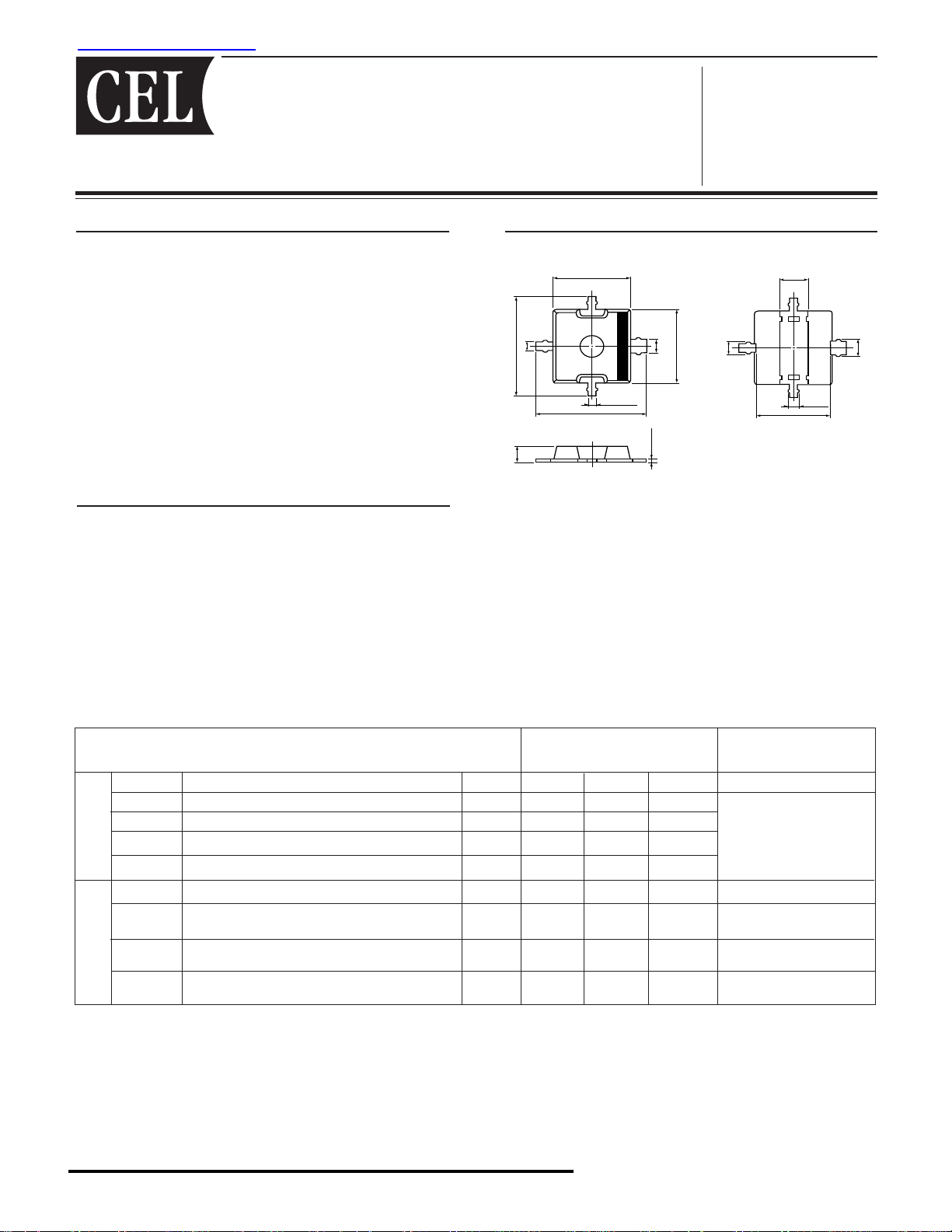
OUTLINE DIMENSIONS (Units in mm)
PACKAGE OUTLINE 79A
4.2 MAX
Source
Gate
5.7 MAX
0.6 – 0.15
0.9 – 0.2
Note: Unless otherwise specified, tolerance is ±0.2 mm
I
T
5.7 MAX
X
9
0.4 – 0.15
Drain
0.2 – 0.1
4.4 MAX
0.8 – 0.15
Gate
1.0 MAX
1.5 – 0.2
3.6 – 0.2
BOTTOM VIEW
Source
0.8 MAX
Drain
MAX
1.2
ELECTRICAL CHARACTERISTICS (TC = 25°C)
PART NUMBER NE6510179A
PACKAGE OUTLINE 79A
SYMBOLS CHARACTERISTICS UNITS MIN TYP MAX TEST CONDITIONS
POUT Output Power dBm 31.5 32.5
GL Linear Gain
ηADD Power Added Efficiency % 50 58
Functional
Characteristics
ID Drain Current A 0.72
IDSS Saturated Drain Current A 2.4 VDS = 2.5 V; VGS = 0 V
VP Pinch-Off Voltage V -2.0 -0.4 VDS = 2.5 V; ID = 14 mA
RTH Thermal Resistance °C/W 5 8 Channel to Case
Electrical DC
Characteristics
BVGD Gate to Drain Breakdown Voltage V 12 IGD = 14 mA
Notes:
1. Pin = 0 dBm
2. DC performance is tested 100% . Several samples per wafer are tested for RF performance. Wafer rejection criteria for standard devices is 1
reject for several samples.
1
dB 10.0
f = 1900 MHz, VDS = 3.5 V,
Pin = +25 dBm, Rg = 100 Ω
IDSQ = 200 mA (RF OFF)
California Eastern Laboratories
2
NE6510179A
TYPICAL RF PERFORMANCE FOR REFERENCE (NOT SPECIFIED) (TC = 25°C)
SYMBOLS CHARACTERISTICS UNITS MIN TYP MAX TEST CONDITIONS
OUT Output Power dBm 35.0
P
G
ηADD Power Added Efficiency % 56
D Drain Current A 1.2
I
P
OUT Output Power dBm 31.5
G
ηADD Power Added Efficiency % 70
I
D Drain Current A 0.53
Notes:
1. Pin = 0 dBm
L Linear Gain
L Linear Gain
1
1
dB 10.0
dB 15.0
f = 1900 MHz, VDS = 5.0 V,
Pin = +25 dBm, Rg = 100 Ω
IDSQ = 200 mA (RF OFF)
f = 900 MHz, V
Pin = +20 dBm, Rg = 100 Ω
DSQ = 200 mA (RF OFF)
I
DS = 3.5 V,
ABSOLUTE MAXIMUM RATINGS1 (TC = 25 °C)
SYMBOLS PARAMETERS UNITS RATINGS
VDS Drain to Source Voltage V 8
VGS Gate to Source Voltage V -4
IDS Drain Current A 2.8
IGS Gate Current (IGF, IGR) mA±25
PT Total Power Dissipation
TCH Channel Temperature °C 150
TSTG Storage Temperature °C -65 to +150
Note:
1. Operation in excess of any one of these parameters may result
in permanent damage.
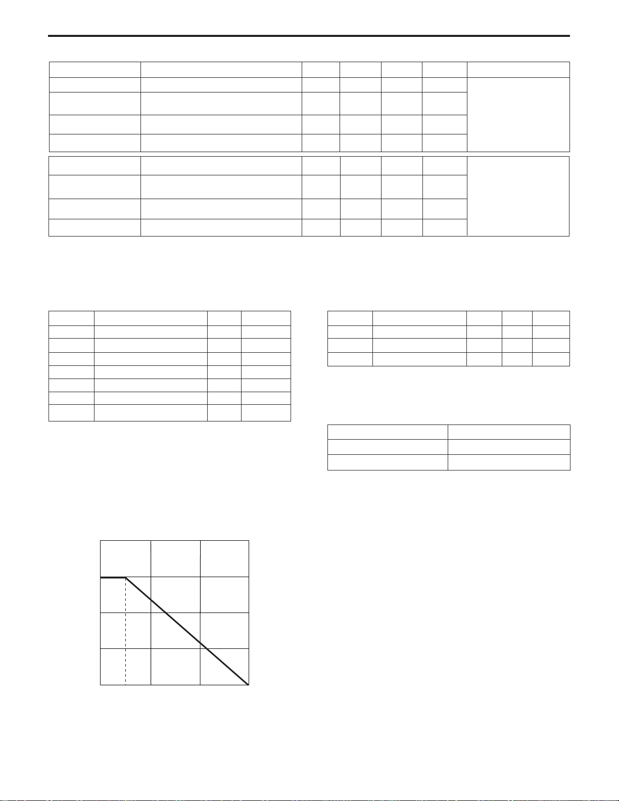
TOTAL POWER DISSIPATION vs.
CASE TEMPERATURE
20
(W)
D
15
2
W15
RECOMMENDED OPERATING LIMITS
SYMBOLS PARAMETERS UNITS TYP MAX
VDS Drain to Source Voltage V 3.5 6.0
TCH Channel Temperature °C +125
GCOMP Gain Compression
Note:
1. Recommended maximum gain compression is 3.0 dB at
VDS > 4.2 V.
ORDERING INFORMATION
PART NUMBER QTY
NE6510179A-T1-A 1 K/Reel
NE6510179A-A Bulk, 100 piece min.
1
dB 3.0
10
5
Total Power Dissipation, P
0
25°C
Case Temperature, TC (°C)
RTH = 8°C/W
15010050
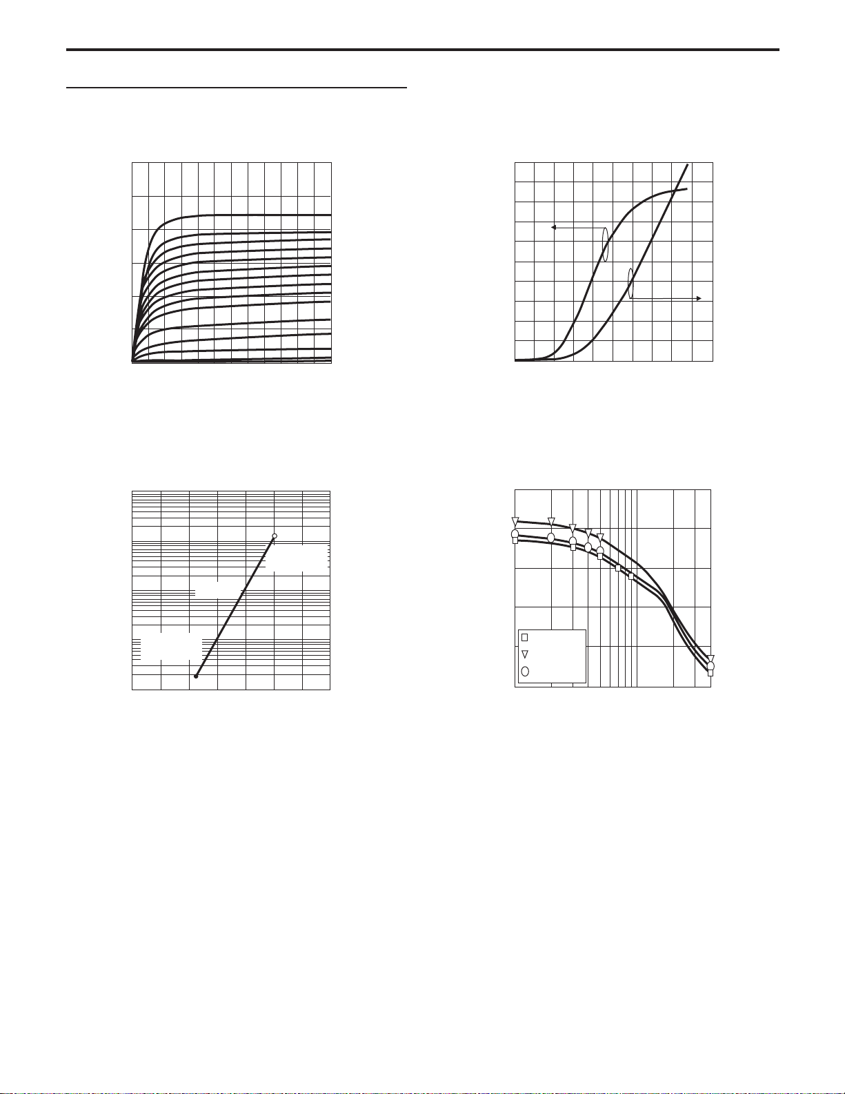
TYPICAL PERFORMANCE CURVES (TA = 25°C)
2.00
1.50
1.00
0.50
2.50
0
0.8
0.6
0.4
0.2
1.00
0
-.80-1.0 -.60 -.20 0.00-.40
NE6510179A
3
2.5
(A)
D
2.0
1.5
1.0
Drain Current, I
0.5
0
012 3456
1.0E+07
1.0E+06
1.0E+05
DRAIN CURRENT vs.
DRAIN VOLTAGE
Drain Voltage, VD (V)
ARRHENIUS PLOTS vs.
JUNCTION TEMPERATURE
1.35E+06 Hrs
(T
CH
= 110°C)
EA = 1.0EV
VGS =
0 V
-0.2 V
-0.4 V
-0.6 V
-0.8 V
-1.0 V
TRANSCONDUCTANCE AND DRAIN
CURRENT vs. GATE VOLTAGE
(mS)
M
Transconductance, G
Gate Voltage, G
MAXIMUM AVAILABLE GAIN vs.
30
(dB)
25
MAG
20
15
FREQUENCY
V (V)
(A)
D
Drain Current, I
1.0E+04
1805 Hrs
(T
CH
= 217°C)
Arrhenius Plots, MTTF (hours)
1.0E+03
1.81.6 2 2.42.2 2.6 32.8
Junction Temperature, T/TCH (1/K/1000)
2.2 V, 200 mA
10
4.6 V, 300 mA
Maximum Available Gain, G
3.5 V, 150 mA
5
0.1 4.0
Frequency, GHz

NE6510179A
TYPICAL SCATTERING PARAMETERS
(TA = 25°C)
Note: This file and many other s-parameter files can be downloaded from www.cel.com
j25
j10
10 25 50 100
0
-j10
-j25
j50
-j50
j100
-j100
0
Coordinates in Ohms
Frequency in GHz
VD = 3.5 V, ID = 150 mA
120°
150°
180°
-150°
-120°
90°
60°
30°
0°
-30°
-60°
-90°
NE6510179A
VD = 3.5 V, ID = 150 mA
FREQUENCY S11 S21 S12 S22 K MAG
GHz MAG ANG MAG ANG MAG ANG MAG ANG (dB)
0.50 0.956 179.67 2.813 82.32 0.018 5.20 0.842 176.48 0.29 21.87
0.60 0.955 177.71 2.343 79.83 0.018 5.02 0.842 175.21 0.34 21.09
0.70 0.956 175.93 2.016 77.44 0.018 5.41 0.843 173.93 0.40 20.38
0.80 0.955 174.33 1.765 75.21 0.018 5.58 0.843 172.76 0.46 19.81
0.90 0.955 172.86 1.573 73.00 0.019 5.93 0.842 171.63 0.51 19.24
1.00 0.955 171.45 1.418 70.78 0.019 6.32 0.842 170.47 0.57 18.79
1.10 0.955 170.09 1.289 68.54 0.019 6.08 0.841 169.22 0.62 18.33
1.20 0.954 168.81 1.187 66.57 0.019 6.55 0.843 168.26 0.67 17.95
1.30 0.954 167.51 1.097 64.47 0.019 6.48 0.842 167.19 0.72 17.59
1.40 0.953 166.27 1.021 62.40 0.019 6.73 0.842 166.12 0.78 17.26
1.50 0.953 165.06 0.955 60.35 0.019 6.94 0.843 165.06 0.82 16.92
1.60 0.953 163.84 0.898 58.36 0.019 6.98 0.843 164.05 0.88 16.65
1.70 0.953 162.63 0.847 56.38 0.020 7.33 0.843 163.06 0.92 16.36
1.80 0.952 161.41 0.802 54.34 0.020 7.16 0.842 161.99 0.98 16.12
1.90 0.951 160.23 0.761 52.35 0.020 7.48 0.844 160.95 1.05 14.59
2.00 0.951 159.05 0.726 50.45 0.020 8.27 0.844 159.99 1.10 13.76
2.10 0.952 157.87 0.693 48.50 0.020 8.79 0.845 159.02 1.13 13.19
2.20 0.951 156.61 0.662 46.53 0.020 8.70 0.844 158.03 1.20 12.48
2.30 0.951 155.50 0.635 44.55 0.020 8.69 0.845 157.05 1.23 12.10
2.40 0.950 154.36 0.611 42.67 0.020 8.71 0.846 156.09 1.27 11.66
2.50 0.950 153.22 0.587 40.91 0.020 8.92 0.847 155.25 1.31 11.27
2.60 0.950 152.11 0.565 39.04 0.020 8.87 0.847 154.33 1.37 10.81
2.70 0.950 150.95 0.545 37.19 0.020 9.41 0.848 153.36 1.41 10.49
2.80 0.950 149.81 0.528 35.36 0.021 9.87 0.850 152.46 1.44 10.17
2.90 0.949 148.69 0.510 33.69 0.020 10.32 0.852 151.70 1.50 9.81
3.00 0.949 147.51 0.494 31.91 0.021 10.98 0.852 150.82 1.52 9.50
3.10 0.949 146.33 0.478 30.21 0.021 11.59 0.854 149.99 1.59 9.17
3.20 0.949 145.20 0.465 28.41 0.021 12.25 0.855 149.11 1.58 8.94
3.30 0.950 144.05 0.452 26.80 0.021 13.46 0.857 148.32 1.61 8.71
3.40 0.949 142.93 0.439 25.05 0.022 13.17 0.858 147.55 1.62 8.41
3.50 0.949 141.85 0.427 23.40 0.022 13.36 0.860 146.79 1.64 8.21
3.60 0.949 140.70 0.416 21.75 0.022 13.56 0.862 146.14 1.64 8.00
3.70 0.949 139.60 0.405 20.23 0.023 13.89 0.864 145.53 1.64 7.85
3.80 0.949 138.47 0.394 18.70 0.023 13.96 0.865 145.01 1.65 7.64
3.90 0.951 137.45 0.384 17.31 0.023 14.08 0.869 144.58 1.59 7.67
4.00 0.950 136.38 0.374 15.99 0.023 14.68 0.875 144.34 1.59 7.50
Note:
1. Gain Calculation:
MAG =
|S
21
|
12
|
|S
(
K ±
2
K - 1
).
When K ≤ 1, MAG is undefined and MSG values are used.
MAG = Maximum Available Gain
MSG = Maximum Stable Gain
MSG =
21
|
|S
, K =
|S
12
|
2
1 + | ∆ | - |S
2 |S
12 S21
11
2
| - |S22|
|
2
∆ = S
,
11 S22
- S21 S
1
12

NE6510179A
TYPICAL SCATTERING PARAMETERS
(TA = 25°C)
Note: This file and many other s-parameter files can be downloaded from www.cel.com
j25
j10
10 25 50 100
0
-j10
-j25
j50
-j50
j100
-j100
0
Coordinates in Ohms
Frequency in GHz
D = 5.0 V, ID = 300 mA
V
-20
-22.5
-26
-32
8
14
17.5
20
NE6510179A
VD = 5.0 V, ID = 300 mA
FREQUENCY S11 S21 S12 S22 K MAG
GHz MAG ANG MAG ANG MAG ANG MAG ANG (dB)
0.50 0.964 179.30 3.090 82.99 0.013 11.07 0.863 175.80 0.38 23.76
0.60 0.963 177.40 2.574 80.69 0.013 12.04 0.862 174.60 0.45 22.97
0.70 0.964 175.60 2.215 78.48 0.013 13.41 0.863 173.30 0.52 22.31
0.80 0.963 174.00 1.940 76.44 0.013 14.52 0.863 172.10 0.59 21.74
0.90 0.963 172.60 1.730 74.41 0.014 15.48 0.862 171.00 0.63 20.92
1.00 0.962 171.20 1.559 72.36 0.014 16.81 0.862 169.90 0.71 20.47
1.10 0.962 169.80 1.418 70.30 0.014 17.13 0.861 164.30 0.77 20.06
1.20 0.962 168.50 1.306 68.47 0.014 18.35 0.862 167.60 0.83 19.70
1.30 0.962 167.20 1.207 66.55 0.015 18.76 0.861 166.50 0.85 19.06
1.40 0.961 166.00 1.124 64.61 0.015 19.61 0.861 165.40 0.92 18.75
1.50 0.961 164.80 1.053 62.72 0.015 20.22 0.861 164.30 0.97 18.46
1.60 0.960 163.60 0.990 60.89 0.015 20.71 0.862 163.30 1.03 17.10
1.70 0.960 162.40 0.934 59.08 0.016 21.61 0.861 162.30 1.05 16.30
1.80 0.960 161.10 0.885 57.16 0.016 21.54 0.860 161.20 1.10 15.55
1.90 0.959 159.90 0.841 55.31 0.016 22.43 0.861 160.10 1.16 14.76
2.00 0.959 158.80 0.803 53.56 0.016 23.77 0.861 159.10 1.22 14.17
2.10 0.959 157.60 0.766 51.76 0.017 24.20 0.861 158.20 1.22 13.71
2.20 0.958 156.30 0.733 49.92 0.017 24.45 0.859 157.20 1.29 13.09
2.30 0.958 155.20 0.704 48.04 0.017 24.16 0.860 156.10 1.32 12.76
2.40 0.957 154.00 0.677 46.31 0.018 24.58 0.862 155.10 1.33 12.33
2.50 0.957 152.90 0.652 44.72 0.018 24.86 0.863 154.30 1.36 11.99
2.60 0.957 151.80 0.627 42.98 0.018 24.96 0.861 153.40 1.42 11.58
2.70 0.957 150.60 0.606 41.20 0.018 25.58 0.862 152.40 1.46 11.27
2.80 0.957 149.50 0.587 39.47 0.019 25.67 0.864 151.40 1.43 11.01
2.90 0.956 148.30 0.568 37.95 0.019 26.27 0.865 150.70 1.49 10.63
3.00 0.956 147.20 0.550 36.32 0.019 27.34 0.865 149.80 1.54 10.30
3.10 0.956 146.00 0.534 34.72 0.020 28.08 0.868 149.00 1.52 10.01
3.20 0.956 144.80 0.519 32.99 0.020 28.08 0.868 148.00 1.54 9.81
3.30 0.957 143.70 0.505 31.47 0.021 29.01 0.869 147.20 1.51 9.61
3.40 0.955 142.50 0.491 29.85 0.021 28.15 0.869 146.50 1.57 9.24
3.50 0.955 141.50 0.478 28.29 0.022 28.47 0.870 145.70 1.55 8.99
3.60 0.955 140.30 0.467 26.73 0.022 28.09 0.873 145.00 1.55 8.89
3.70 0.955 139.20 0.455 25.35 0.023 28.10 0.873 144.40 1.54 8.64
3.80 0.956 138.00 0.443 23.91 0.023 27.80 0.874 143.90 1.54 8.53
3.90 0.957 137.00 0.431 22.54 0.024 27.69 0.877 143.50 1.48 8.44
4.00 0.956 135.90 0.421 21.29 0.024 27.86 0.883 143.20 1.49 8.32
Note:
1. Gain Calculation:
MAG =
|S
21
|
(
12
|
|S
K ±
2
K - 1
).
When K ≤ 1, MAG is undefined and MSG values are used.
MAG = Maximum Available Gain
MSG = Maximum Stable Gain
MSG =
21
|
|S
, K =
|S
12
|
2
1 + | ∆ | - |S
2 |S
12 S21
11
2
| - |S22|
|
2
∆ = S
,
11 S22
- S21 S
1
12

APPLICATION CIRCUIT (1.93-1.99 GHz)
VG
C3
C9
C11
P1
GND
J3
NE6510179A
V
D
J4
GND
C2
C8
C10
G
V
RF Input
J3
J1
C5
RF
C4
C12
C1
OUT
RF
J2
Contact CEL Engineering for artwork
and more detailed information.
C13
IN
J1
R1
C5
100637
C6
T I
8 X
U1
NE65XXX79A-EV
.034
J4
V
D
L = .890
W = .010
L = .874
W = .010
C2
C8 C10 C12C13 C11 C9 C3
R1
NE6510179A
J2
RF Output
L = .280
W = .050
C4
L = .260
W = .050
C1
1 TF-100637 TEST CIRCUIT BLK 17
4 2-56 X 3/16 PHILLIPS PAN HEAD 16
2 MA101J C2, C3 CASE 1 100 pF CAP MURATA 15
1 MCR03J200 R1 0603 20 OHM RESISTOR ROHM 14
1 100A6RBCP150X C14 NOT USED CASE A 6.8 pF CAP ATC 13
1 100A4R3CP150X C4 CASE A 4.3 pF CAP ATC 12
2 100A240CP150X C5. C1 CASE A 24 pF CAP ATC 11
1 100A4R7CP150X C6 CASE A 4.7 pF CAP ATC 10
1 100A1RBCP150X C7 NOT USED CASE A 1.8 pF CAP ATC 9
2 TAJB475K010R C12, C13 CASE B 4.7 µF CAP AVX 8
2 GRM40X7R104K025BL C10, C11 0805 .1 µF CAP MURATA 7
2 GRM40C0G102J050BD C8, C9 0805 1000 pF CAP MURATA 6
1 NE6510179A U1 IC NEC 5
1 703401 P1 GROUND LUG CONCORD 4
1 1250-003 J3, J4 FEEDTHRU MURATA 3
2 2052-5636-02 J1, J2 FLANGE MOUNT JACK RECEPTACLE 2

NE6510179A
TYPICAL APPLICATION CIRCUIT PERFORMANCE at VDS = 3 V and VDS = 5 V
PAE & GAIN
vs. OUTPUT POWER
14
12
10
8
(dB)
A
6
Gain, G
4
2
FC = 1.96 GHz, VDS
0
20 22 24 26 28 30 32 34
= 3 V
Gain, I
Gain, I
PAE, I
PAE, I
Output Power, POUT (dBm)
GAIN & SATURATED POWER
vs. FREQUENCY
16
14
(dB)
A
12
DSQ
DSQ
DSQ
DSQ
= 200 mA
= 600 mA
= 200 mA
= 600 mA
PAE & GAIN
vs. OUTPUT POWER
60
50
40
30
PAE (%)
20
10
0
14
FC = 1.96 GHz, VDS = 5 V
12
10
8
(dB)
A
6
Gain, G
4
Gain, IDSQ = 200 mA
Gain, I
2
0
20 22 2624 28 30 32 34 36
PAE, I
PAE, I
DSQ = 600 mA
DSQ = 200 mA
DSQ = 600 mA
50
45
40
35
30
25
PAE (%)
20
15
10
5
0
Output Power, POUT (dBm)
GAIN & SATURATED POWER
vs. FREQUENCY
33
32
(dBm)
SAT
31
(dB)
A
16
14
12
36
35
(dBm)
SAT
34
Gain, G
10
P
OUT
= 16 dB for Gain
29 dB for P
VDS = 3 V
8
SAT
1.90 1.92 1.94 1.96 1.98 2.00 2.02
Gain, I
Gain, I
P
OUT
OUT
P
DSQ
DSQ
, I
DSQ
, I
DSQ
Frequency, f (GHz)
THIRD ORDER INTERMODULATION
vs. TOTAL OUTPUT POWER
15
FC = 1.96 GHz, P
(dBc)
3
VDS = 3 V
20
25
30
35
40
45
20 21 22 23 24 25 26 27 28 29 30
Third Order Intermodulation Distortion, IM
Total Output Power, POUT (dBm)
OUT
= Each Tone
IDSQ = 100 mA
I
DSQ = 200 mA
I
DSQ = 400 mA
DSQ = 600 mA
I
I
DSQ = 800 mA
= 100 mA
= 800 mA
= 100 mA
= 800 mA
Gain, G
= 100 mA
= 800 mA
33
Saturated Power, P
32
30
Saturated Power, P
29
10
P
OUT
= 16 dB for Gain
29 dB for P
SAT
VDS = 5 V
8
1.91 1.92 1.94 1.96 1.98 2.00 2.02
Gain, I
Gain, I
OUT
P
OUT
P
, I
, I
DSQ
DSQ
DSQ
DSQ
= 100 mA
= 800 mA
Frequency, f (GHz)
THIRD ORDER INTERMODULATION
vs. TOTAL OUTPUT POWER
15
I
DSQ
(dBc)
3
20
25
30
35
40
45
Third Order Intermodulation Distortion, IM
= 100 mA
DSQ
= 200 mA
I
DSQ
= 400 mA
I
I
DSQ
= 600 mA
I
DSQ
= 800 mA
FC = 1.96 GHz, P
OUT
= Each Tone
VDS = 5 V
20 21 22 23 24 25 26 27 28 29 30
Total Output Power, POUT (dBm)

TYPICAL APPLICATION CIRCUIT PERFORMANCE at VDS = 3 V and VDS = 5 V
NE6510179A
ACPR
vs. OUTPUT POWER
35
ACPR1
885 KHz
(dBc)
40
3
45
ACPR2
50
1.25 MHz
55
60
Third Order Intermodulation Distortion, IM
FC = 1.96 GHz, VDS
= 3 V
,
64 CH IS95 CDMA
65
23 24 25 26 27 28 29 30 31 32 33
Output Power, POUT (dBm)
100 mA
200 mA
400 mA
600 mA
800 mA
ACPR
vs. OUTPUT POWER
35
FC = 1.96 GHz, VDS
64 CH IS95 CDMA
40
(dBc)
3
= 5 V
ACPR1
885 KHz
45
50
55
I
60
Third Order Intermodulation Distortion, IM
65
DSQ
I
DSQ
DSQ
I
DSQ
I
DSQ
I
23 25 27 29 31 33 35
Output Power, POUT (dBm)
ACPR2
1.25 MHz
= 100 mA
= 200 mA
= 400 mA
= 600 mA
= 800 mA

NE6510179A
.
NONLINEAR MODEL
SCHEMATIC
GATE
LGX
0.001 nH
CGS PKG
0.1 pF
Q1
LG
0.75 nH
FET NONLINEAR MODEL PARAMETERS
Parameters Q1 Parameters Q1
VTO -0.756 RG 0.05
VTOSC 0 RD 0.001
ALPHA 2 RS 0.001
BETA 2.245 RGMET 0
GAMMA 0 KF 0
GAMMADC
DELTA 0 XTI 3
CGSO
CGDO
DELTA1 0.3
DELTA2 0.2
(1) Series IV Libra TOM Model
The parameter in Libra corresponds to the parameter in PSpice:
(2) GAMMADC GAMMA
(3) CGSO CGS
(4) CGDO CGD
(2)
0.01 AF 1
Q 1.7 TNOM 27
VBI 0.6 EG 1.43
IS 1e-16 VTOTC 0
N 1 BETATCE 0
RIS 0 FFE 1
RID 0
TAU 10e-12
CDS 0.5e-12
RDB 0.001
CBS 0
(3)
(4)
20e-12
4e-12
FC 0.5
VBR Infinity
(1)
LD LDX
RSX
0.05 ohms
LSX
0.001 nH
SOURCE
RDX
0.2 ohms
RDBX
400 ohms
CBSX
100 pF
0.65 nH 0.01 nH
CDS PKG
0.1 pF
DRAIN
UNITS
Parameter Units
capacitance picofarads
inductance nanohenries
resistance ohms
MODEL RANGE
Frequency: 0.5 to 4 GHz
Bias: VDS = 2.2 V to 5 V, ID = 150 mA to 300 mA
Date: 3/29/2000
Life Support Applications
These NEC products are not intended for use in life support devices, appliances, or systems where the malfunction of these products can reasonably
be expected to result in personal injury. The customers of CEL using or selling these products for use in such applications do so at their own risk and
agree to fully indemnify CEL for all damages resulting from such improper use or sale.
A Business Partner of NEC Compound Semiconductor Devices, Ltd
11/04/2002

4590 Patrick Henry Drive
(
Santa Clara, CA 95054-1817
Telephone: (408) 919-2500
Facsimile:
408) 988-0279
Subject: Compliance with EU Directives
CEL certifies, to its knowledge, that semiconductor and laser products detailed below are compliant
with the requirements of European Union (EU) Directive 2002/95/EC Restriction on Use of Hazardous
Substances in electrical and electronic equipment (RoHS) and the requirements of EU Directive
2003/11/EC Restriction on Penta and Octa BDE.
CEL Pb-free products have the same base part number with a suffix added. The suffix –A indicates
that the device is Pb-free. The –AZ suffix is used to designate devices containing Pb which are
exempted from the requirement of RoHS directive (*). In all cases the devices have Pb-free terminals.
All devices with these suffixes meet the requirements of the RoHS directive.
This status is based on CEL’s understanding of the EU Directives and knowledge of the materials that
go into its products as of the date of disclosure of this information.
Restricted Substance
per RoHS
Lead (Pb) < 1000 PPM
Concentration Limit per RoHS
(values are not yet fixed)
Concentration contained
in CEL devices
-A -AZ
Not Detected (*)
Mercury < 1000 PPM Not Detected
Cadmium < 100 PPM Not Detected
Hexavalent Chromium < 1000 PPM Not Detected
PBB < 1000 PPM Not Detected
PBDE < 1000 PPM Not Detected
If you should have any additional questions regarding our devices and compliance to environmental
standards, please do not hesitate to contact your local representative.
Important Information and Disclaimer: Information provided by CEL on its website or in other communications concerting the substance
content of its products represents knowledge and belief as of the date that it is provided. CEL bases its knowledge and belief on information
provided by third parties and makes no representation or warranty as to the accuracy of such information. Efforts are underway to better
integrate information from third parties. CEL has taken and continues to take reasonable steps to provide representative and accurate
information but may not have conducted destructive testing or chemical analysis on incoming materials and chemicals. CEL and CEL
suppliers consider certain information to be proprietary, and thus CAS numbers and other limited information may not be available for
release.
In no event shall CEL’s liability arising out of such information exceed the total purchase price of the CEL part(s) at issue sold by CEL to
customer on an annual basis.
See CEL Terms and Conditions for additional clarification of warranties and liability.
 Loading...