

n
查询NE5511279A供应商
NEC'S 7.5 V UHF BAND
RF POWER SILICON LD-MOS FET
FEATURES
• HIGH OUTPUT POWER:
Pout = 40.0 dBm TYP., f = 900 MHz, VDS = 7.5 V,
Pout = 40.5 dBm TYP., f = 460 MHz, VDS = 7.5 V,
• HIGH POWER ADDED EFFICIENCY:
ηadd = 48% TYP., f = 900 MHz, VDS = 7.5 V,
ηadd = 50% TYP., f = 460 MHz, VDS = 7.5 V,
• HIGH LINEAR GAIN:
GL = 15.0 dB TYP., f = 900 MHz, VDS = 7.5 V,
GL = 18.5 dB TYP., f = 460 MHz, VDS = 7.5 V,
• SURFACE MOUNT PACKAGE:
5.7 x 5.7 x 1.1 mm MAX
• SINGLE SUPPLY:
VDS = 2.8 to 8.0 V
APPLICATIONS
• UHF RADIO SYSTEMS
• CELLULAR REPEATERS
• TWO-WAY RADIOS
• FRS/GMRS
• FIXED WIRELESS
NE5511279A
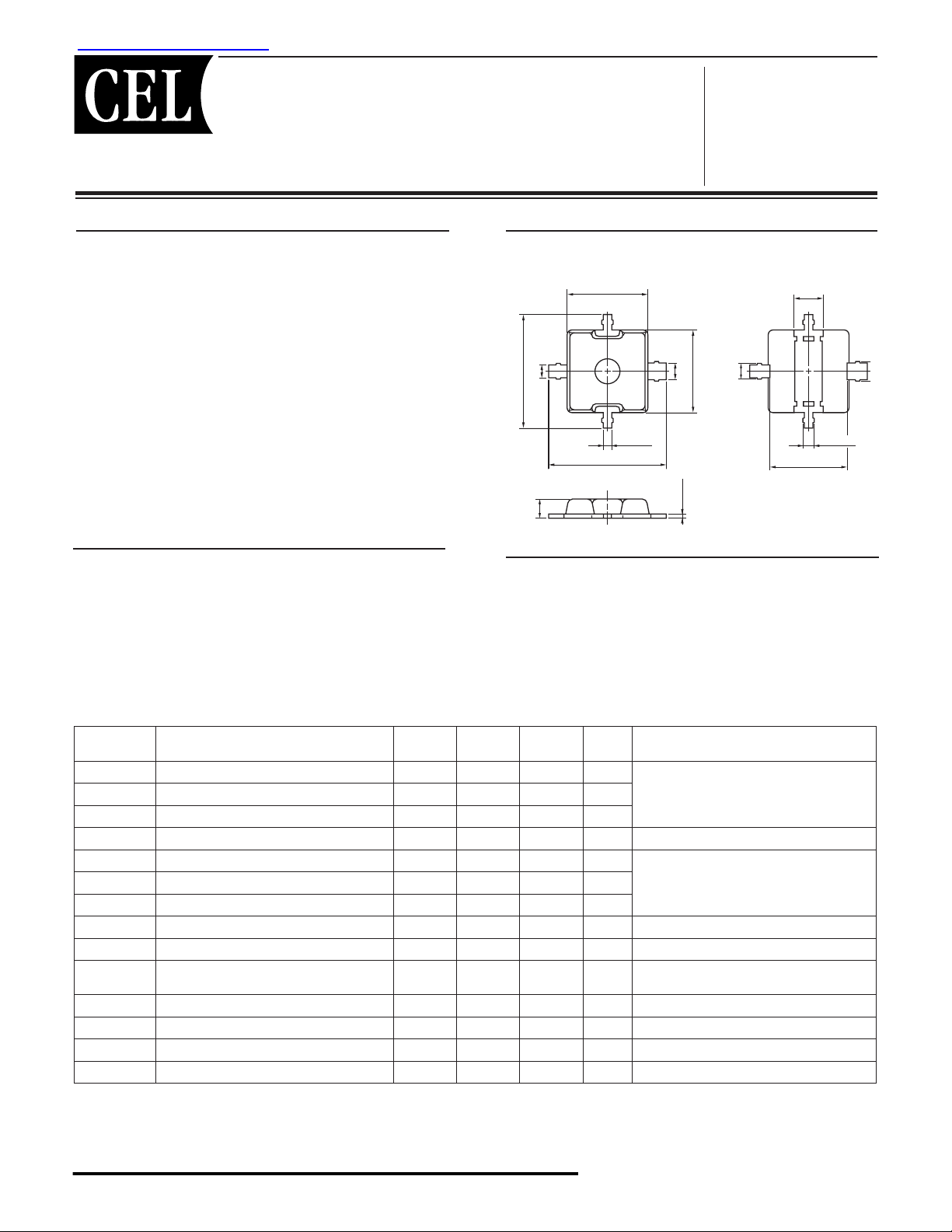
OUTLINE DIMENSIONS (Units in mm)
PACKAGE OUTLINE 79A
Gate
1.0 MAX.
(Bottom View)
1.5±0.2
Source
Drai
0.8 MAX.
3.6±0.2
4.2 MAX.
Source
0.6±0.15
5.7 MAX.
0.9±0.2
Gate
W 3
5.7 MAX.
21001
0.4±0.15
Drain
0.8±0.15
0.2±0.1
4.4 MAX.
DESCRIPTION
NEC's NE5511279A is an N-Channel silicon power laterally
dif fused MOSFET spe cial ly designed as the transmission
power amplifi er for 7.5 V radio systems. Die are man u -
fac tured us ing NEC's NEWMOS1 tech nol o gy and housed in
a surface mount pack age. This device can deliver 40.0 dBm
output power with 48% power added effi ciency at 900 MHz
using a 7.5 V supply voltage.
ELECTRICAL CHARACTERISTICS
(TA = 25°C)
SYMBOL PARAMETER MIN TYP MAX UNIT TEST CONDITIONS
−
dBm
f = 900 MHz, V
−
−
−
−
−
−
−
APin = 27 dBm,
I
DSQ
%
= 400 mA (RF OFF)
dB Pin = 5 dBm
dBm
f = 460 MHz, V
APin = 25 dBm,
I
DSQ
%
= 400 mA (RF OFF)
dB Pin = 5 dBm
100 nA VGS = 6.0 V
DS
100 nA V
−
°C/W Channel to Case
−
−
SVDS = 3.5 V, IDS = 900 mA
VI
= 8.5 V
DSS
= 15 µA
DS
= 7.5 V,
DS
= 7.5 V,
BV
P
η
P
η
I
I
I
G
I
G
GSS
DSS
V
R
g
add
add
out
D
out
D
Output Power 38.5 40.0
Drain Current
−
2.5
Power Added Effi ciency 42 48
L
Linear Gain
Output Power
Drain Current
Power Added Effi ciency
L
Linear Gain
Gate to Source Leak Current
Drain to Source Leakage Current
(Zero Gate Voltage Drain Current)
th
Gate Threshold Voltage 1.0 1.5 2.0 V VDS = 4.8 V, IDS = 1.5 mA
th
Thermal Resistance
m
Transconductance
DSS
Drain to Source Breakdown Voltage 20 24
−
−
−
−
−
15.0
40.5
2.75
50
18.5
−−
−−
−
−
5
2.3
Notes:
DC performance is 100% tested. RF performance is tested on several samples per wafer.
Wafer rejection criteria for standard devices is 1 reject for several samples.
California Eastern Laboratories
NE5511279A
ABSOLUTE MAXIMUM RATINGS1 (TA = 25 °C)
SYMBOLS PARAMETERS UNITS RATINGS
V
DS Drain Supply Voltage
GS Gate Supply Voltage V 6.0
V
D Drain Current A 3.0
I
2
V 20.0
PTOT Total Power Dissipation W 20
T
CH Channel Temperature °C 125
STG Storage Temperature °C -55 to +125
T
Note:
1. Operation in excess of any one of these parameters may result
in permanent damage.
2. VDS must be used under 12 V on RF operation.
P.C.B. LAYOUT (Units in mm)
79A PACKAGE
4.0
1.7
Source
Gate Drain
5.9
1.0
0.5
1.2
RECOMMENDED OPERATING LIMITS
SYMBOLS PARAMETERS UNITS TYP MAX
VDS Drain to Source Voltage V 7.5 8.0
VGS Gate Supply Voltage V 2.0 3.0
DS Drain Current
I
1
A 2.5 3.0
PIN Input Power dBm 27 30
f = 900 MHz, VDS = 7.5 V
ORDERING INFORMATION
PART NUMBER QTY
NE5511279A-T1 • 12 mm wide embossed taping.
• Gate pin faces the perforation side of
the tape.
• 1 Kpcs/Reel
NE5511279A-T1A • 12 mm wide embossed taping.
• Gate pin faces the perforation side of
the tape.
• 5 Kpcs/Reel
Through hole φ 0.2 × 33
0.5 0.5
6.1
Note:
Use rosin or other material to prevent solder from penetrating
through-holes.
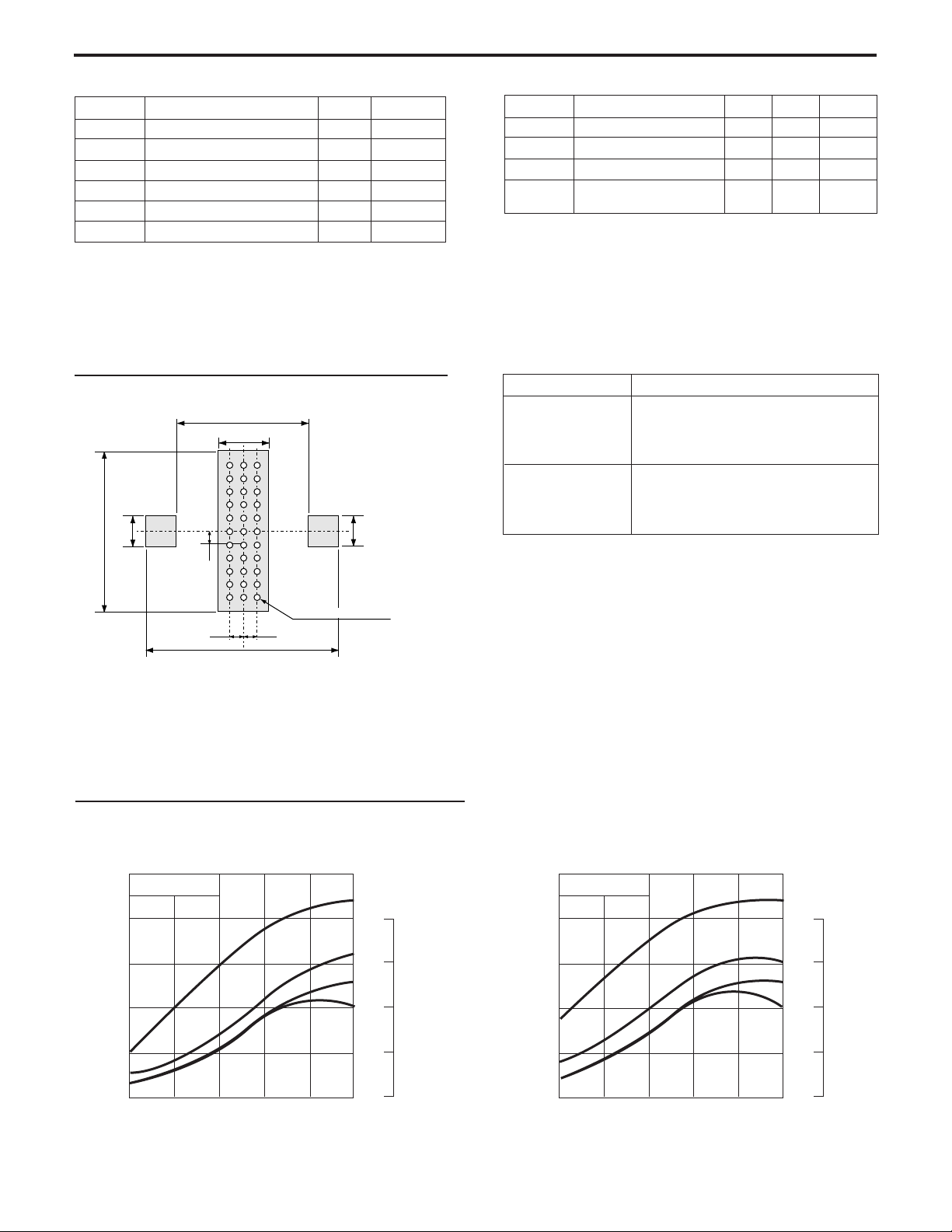
TYPICAL PERFORMANCE CURVES (TA = 25°C)
OUTPUT POWER, DRAIN CURRENT,
η
d, ηadd vs. INPUT POWER
45
f = 900 MHz
40
35
30
25
Output Power, Pout (dBm)
20
10 15 20 25 30 35
P
IDS
ηd
ηadd
5
out
4
100
DS (A)
75
3
50
2
25
1
Drain to Source Current, I
0
0
Drain Effi ciency, ηd (%)
Power Added Effi ciency, ηadd (%)
OUTPUT POWER, DRAIN CURRENT,
ηd, ηadd vs. INPUT POWER
45
f = 460 MHz
40
35
30
25
Output Power, Pout (dBm)
20
10 15 20 25 30 35
P
IDS
ηd
ηadd
5
out
4
100
DS (A)
75
3
50
2
25
1
Drain to Source Current, I
0
0
Drain Effi ciency, ηd (%)
Power Added Effi ciency, ηadd (%)
Input Power,P
in (dBm)
Input Power,P
in (dBm)

RECOMMENDED SOLDERING CONDITIONS
.
This product should be soldered and mounted under the following recommended conditions. For soldering methods
and conditions other than those recommended below, contact your nearby sales offi ce.
Soldering Method Soldering Conditions Condition Symbol
Infrared Refl ow Peak temperature (package surface temperature) : 260°C or below
Time at peak temperature : 10 seconds or less
Time at temperature of 220°C or higher : 60 seconds or less
Preheating time at 120 to 180°C : 120±30 seconds
Maximum number of refl ow processes : 3 times
Maximum chlorine content of rosin fl ux (% mass) : 0.2%(Wt.) or below
NE5511279A
IR260
VPS Peak temperature (package surface temperature) : 215°C or below
Time at temperature of 200°C or higher : 25 to 40 seconds
Preheating time at 120 to 150°C : 30 to 60 seconds
Maximum number of refl ow processes : 3 times
Maximum chlorine content of rosin fl ux (% mass) : 0.2%(Wt.) or below
Wave Soldering Peak temperature (molten solder temperature) : 260°C or below
Time at peak temperature : 10 seconds or less
Preheating temperature (package surface temperature) : 120°C or below
Maximum number of fl ow processes : 1 time
Maximum chlorine content of rosin fl ux (% mass) : 0.2%(Wt.) or below
Partial Heating Peak temperature (pin temperature) : 350°C or below
Soldering time (per pin of device) : 3 seconds or less
Maximum chlorine content of rosin fl ux (% mass) : 0.2%(Wt.) or below
Caution Do not use different soldering methods together (except for partial heating).
VP215
WS260
HS350-P3
Life Support Applications
These NEC products are not intended for use in life support devices, appliances, or systems where the malfunction of these products can reasonably
be expected to result in personal injury. The customers of CEL using or selling these products for use in such applications do so at their own risk and
agree to fully indemnify CEL for all damages resulting from such improper use or sale.
A Business Partner of NEC Compound Semiconductor Devices, Ltd
08/26/2003
 Loading...