


CDMA HX550c, Z720i Service Manual

Z720i Service Manual
Copyrights 2004 ⓒ Pantech & CuritelZ720i

- INDEX -
1. Overview
1.1 General
1.2 Standards & Specification
1.3 Features
2. H/W Part
2.1 H/W Description
2.2 Block Diagram
2.3 One point Fix
2.4 New Function
2.5 New Parts Introduction
2.6 Trouble Shooting Guide
2.7 Circuit Diagram
3. S/W Part
3.1 UI Menu Tree
3.2 Keypad
3.3 Annunciator
3.4 Zapp Me(BREW)
3.5 Camera
3.6 Voice Memo
3.7 Memory information
3.8 Test Code
3.9 Debug Screen
4. PART LIST
5. APPENDIX
- Location Map
- Exploded View
Copyrights 2004 ⓒ Pantech & CuritelZ720i

1. Overview
1.1 General
▶Z720i is base on the CDMA NMT-450 technology. This technology using
the 1.25MHz spread-spectrum of 450MHz band, this CDMA NMT-450
cellular phone provides greatly enhanced voice quality and more
reliable
encoding function.
▶The IFR3500 is a key circuit element in the Rx signal path of CDMA450.
The CDMA receive path is designed to accept a differential IF signal with
CDMA spread spectrum modulation extending ±630KHz from the IF
center frequency. The RFT3100 interface with the MSM5100 and circuits
in
the analog transmit chain of the CDMA450 phone. The RFT3100 up
converts to the IF frequency and puts out a controlled amplitude
differential Tx IF signal. The RFT3100 & IFR3500 are controlled by means
of a three-line Serial Bus Interface(SBI) which is driven by MSM5100.
▶LCD Module consists of Main LCD(128x160Dots,1.8” 65K Color CSTN)
and SUB LCD(96x64Dots B/W CSTN LCD)
▶ 300K CMOS Camera Module supported 30 photo save at QVGA mode
(320x240), Linear 4X Digital Zoom
▶ 16 POLY CMX Melody
▶ PC Sync(USB)
Copyrights 2004 ⓒ Pantech & CuritelZ720i

1.2 Standards & Specification
1.2.1 Standards
▶ Air interface standard : IS-2000
▶ Vocoder : IS-96A,IS-127,IS-733
▶ Data Service : IS-707A
▶ RF specification : IS-98D
▶ OTASP : IS-638A
▶ SMS : IS-637
1.2.2 Specification
▶ POWER SUPPLY Adapter
1) INPUT : CTA-10A, 100-24V(AC) 50/60Hz 0.3A
2) OUTPUT : DC 5.5V, 2000mA
3) CHARGER: inner-charger
▶ BATTERY
TYPE : Ni-ion,1000mAh(553450)
▶ POWER CONSUMPTION
1) NORMAL(Stand-by) : CDMA Mode : 100 mA (During call waiting),
700 ㎃±10% (While busy, LCD On ,based
on Max Pwr(+23 dBm) )
2) Waiting Time : About 120hours
* Field Conditions Applied
* Slot Cycle Index : 2
* Power Consumed in Sleep Mode: less than 1 mA
3) Talk time : Up to 2 hours(@ sct Pwr -100 dBm)
Copyrights 2004 ⓒ Pantech & CuritelZ720i

1.2 Standards & Specification
1.2.2 Specification
▶ Freq. Range : Rx :462.5 ~ 467.475 MHz, Tx :452.5 ~ 457.475 MHz
▶ Bandwidth : 1.25MHz
▶ Channel Frequency
160ch Rx : 463.975MHz, Tx : 453.975MHz
210ch Rx : 465.225MHz, Tx : 455.225MHz
260ch Rx : 466.475MHz, Tx : 456.475MHz
▶ TX maximum output power : 0.2W (23dBm) above
▶ TX minimum output power : -50dBm below
▶ RX Sensitivity : -104dBm below ( at FER = 0.5% )
▶ Single tone Desensitization : -101dBm below ( at FER = 1% )
▶ Rx conducted spurious
Emission
TX Band : -61dBm/1MHz below
RX Band : -81dBm/1MHz below
Out of Band : -47dBm/30kHz below.
▶ Tx conducted spurious
Emission
In Band : -42 dBc/30kHz(fc +/-885kHz)
-54 dBc/30kHz(fc +/-1.98MHz)
Out Band 1~6:less than –47 dBm/30kHz
▶ Static Time Offset : ± 1㎲ below
▶ Traffic Rho : 0.944 above
Copyrights 2004 ⓒ Pantech & CuritelZ720i

1.3 Features
SpecipicationSpecipication
Folder TypeHinge TypeCDMA450Mode
100 gWeight(g)MSM 5100Chip Set
Memory
LCD Module
Camera
SPICOM
128Mb Flash + 32Mb RAM
S : B/W CSTN, 96 X 64
Earpiece : 121dB±2dB @ 1KHz
Vibrator : RPM : MAX 12,000 ±2,000
Fixed AntennaANT
26 KEYKey ButtonM : 1.8”, 65 K CSTN,128X160
1000 mAh Li-IonBattery
Ear-Jack300K CMOS
YesFlash 16 Poly CMXMelody
88 X 47 X 23.8 mmSIZESpeaker : 12.6¢ 500mW
Copyrights 2004 ⓒ Pantech & CuritelZ720i

2. H/W Part
2.1 H/W Description
1) RX PART
▶ DUPLEXER (Rx: D465AK(FIL210) Tx: D455AK(FIL250))
- The duplexer is made up of a TX_Filter and RX_Filter. It is composed of an antenna port, a transmitter port and a receiver
port. The TX-Filter is configured with a SAW bandpass filter. This prevents harmonic spurious emission and leakage from
entering into adjacent channels. The RX-filter is also configured with a SAW bandpass filter. It suppresses the malfunction
of LNA while sufficiently rejecting strong neighboring interferes. Thus the choice of BPF is governed by both the out-of-band
rejection and the in-band loss, with the latter being the more critical parameter. prevents image spurious by transmit carrier
signal. The special matching circuit is adopted to increase the isolation between the transmitter and the receiver. Since large
in-band interferers accompany the received signal even after the duplexer and this large in-band interferes make cross
modulation with the leakage from the transmitter, the isolation between the transmitter and the receiver is very important.
▶ ITM1010 (U210)
- ITM1010 is composed of low noise amplifiers (LNA) and down-conversion mixer. The LNA figures a sufficiently
high IP3 to avoid corruption of the signal by intermodulation products. The IP3 of LNA affects single tone de-sensitization
performance. The LNA is operated ON and OFF by LNA Range signal which come to MSM directly. LNA-ON gain has about
17dB and LNA-OFF gain has about -7dB. The image rejection BPF is configured with a SAW bandpass filter which is the
same filter as the RX-Filter in the duplexer section. Since the image frequency of the received signal is downconverted to the
same IF bands,it is very important to suppress the image. The down-conversion mixer is included in ITM1010 chip. It makes
85.38 MHz IF signal mix RF signal with Local signal.
▶ Rx SAW Filter (FIL220)
- It suppresses the malfunction of LNA while sufficiently rejecting strong neighboring interferes
Copyrights 2004 ⓒ Pantech & CuritelZ720i

▶ IFR3500 (U650)
- IFR3500 receive path is designed to accept a differential IF signal. Rx AGC amplifies controlled by varying the DC voltage
on the Vcontrol input pin attenuates the received CDMA IF signal to provide a constant-amplitude signal to the I/Q down
converter. The AGC’s 90dB dynamic range is available over the full power supply range of the device.
▶ Rx IF SAW Filter (FIL230)
-
The IF Filter attenuates the noise of signal that has been down-converted in the mixer. It is used to extract signals orresponding
to one channel bandwidth.
2) TX PART
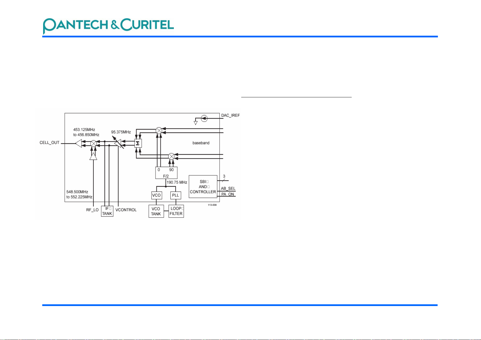
▶ RFT3100(U700)
- The RFT3100 interface with the MSM5100 and circuits in the analog transmit chain of the CDMA450 phone. The RFT3100 up
converts to the IF frequency and puts out a controlled amplitude differential Tx IF signal. The RFT3100 is controlled by means of
a three-line Serial Bus Interface(SBI) which is driven by MSM5100.The RFT3100 includes a programmable Tx PLL for synthesizing
the Tx IF frequency. A temperature-compensated Tx AGC amplifier with 85dB gain range is included in the RFT3100. The transmit
output power level is directly controlled by varying the gain of this Tx AGC amplifier.
▶ Power Amp(U250)
- This is a part to amplify TX power for the last time. It has a direct effect on variable range of –54 dBm ~ +23.5 dBm for ANT
output part. Accordingly, During the call, it consumes most of current supplied and so, it should ensure high efficiency.
▶ Tx Saw Filter (FIL270)
- This is a part to reduce out-band noise and Before PAM amplifies the RF Signal, attenuate in-band noise
Copyrights 2004 ⓒ Pantech & CuritelZ720i

3) LOGIC Parts
▶ MSM5100
- MSM5100 is the ASIC Chip for Baseband Digital Signal Processing of the handset. It implies the integrated
CODEC and supports Integrated Universal Serial Bus(USB) interface. And it has internal Vocoder supporting
13Kbps QCELP and 8Kbps EVRC. Besides it uses ARM7TDMI embedded microprocessor subsystem.
▶ MEMORY
- SHARP’s Product consisted of 128M Flash Memory and 32M Smart combo RAM used to save MSM Boot Code and
NV Data
▶ LCD MODULE
- As Dual CSTN-LCD Module combined Main LCD and Sub LCD, and it has Flash LED and 300K CMOS Camera
Module, Main LCD display 65k color 128 X 160 Dots. Sub LCD display B/W color 96 X 64 Dots.
* MAIN : 1.8”, 65 K CSTN,128X160
* SUB : B/W CSTN, 96 X 64
▶ SPICOM
- SPICOM is combined Receiver, Speaker and Vibrator
# Speaker
* SPL(Sensitivity) : 87dB±2dB, fo : 800Hz ±20% @1V, Nominal input Power : 500mW, Impedance : 8 ohm
# Receiver
* SPL(Sensitivity) : 121dB±2dB @ 1KHz, RIP : 50mW, Impedance : 8ohm
# Vibrator
* RPM : MAX 12,000 ±2,000 Operating Voltage : DC 2.6V ~ 3.6V
Copyrights 2004 ⓒ Pantech & CuritelZ720i

▶ CAMERA Module
- HX-550C adopts 300K CMOS camera module that supports 30 supported 30 photo save at QVGA
mode (320x240), Linear 4X Digital Zoom photo
Copyrights 2004 ⓒ Pantech & CuritelZ720i
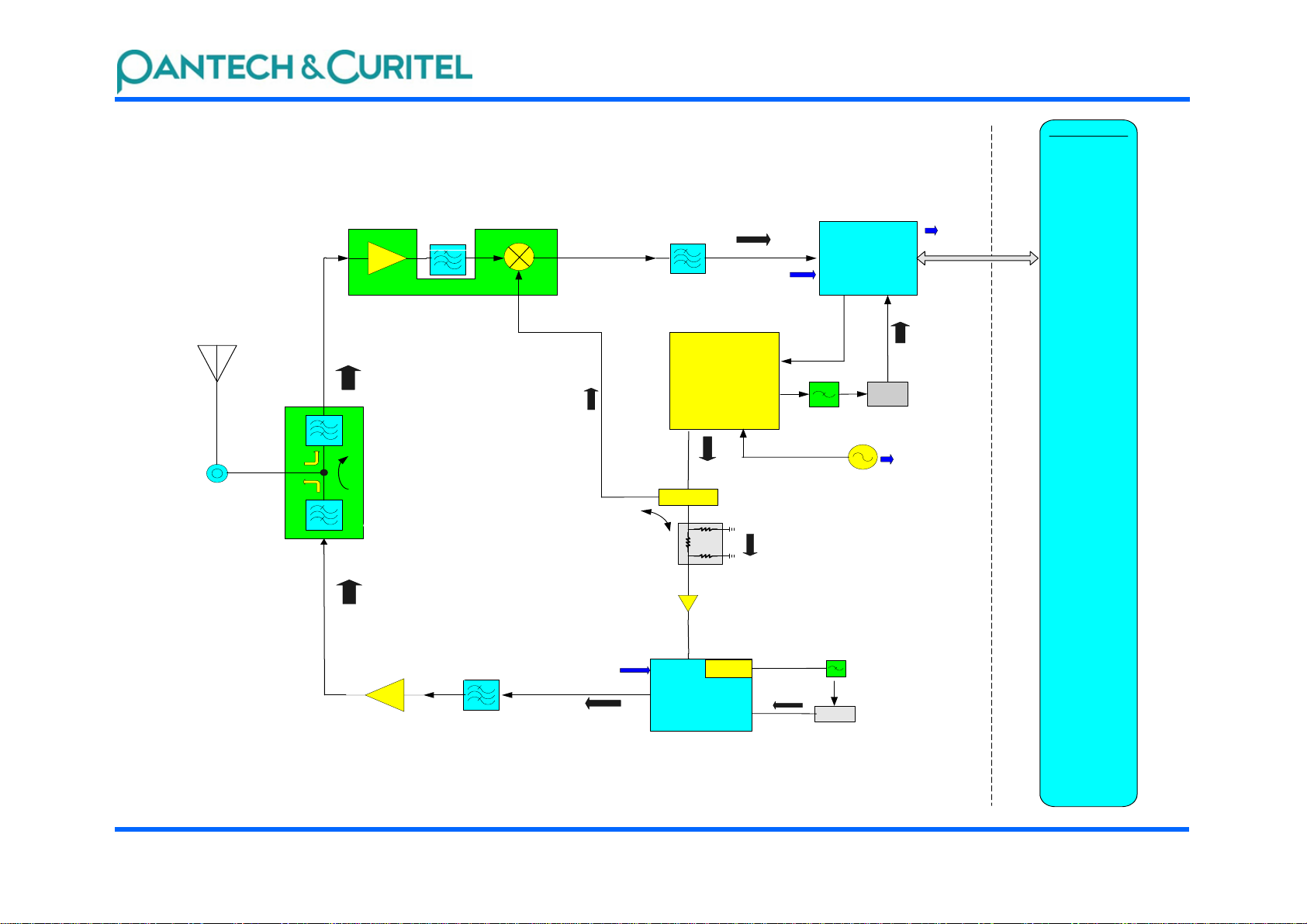
2.2.1 Block Diagram (RF Part)
RF_SA W
RF_SA W
D46 5AK (Sam sun g)
D46 5AK (Sam sun g)
G : - 2.3 ~ -2.7 dB
G : - 2.3 ~ -2.7 dB
REJECTION(452.5~458) :
REJECTION(452.5~458) :
-55 ~ - 64
-55 ~ - 64
LNA
ITM1010(Integrant)
G : 17dB
NF :1.6dB
IIP :9.5dBm
462.500~467.475MHz
RF _SA W
D465AK(SAMSUNG)
G - 2dB
REJECTION(452.5~458) :
-50 ~ - 64
ISO LAT ION : - 50 ~ -6 6dB C
RF _SA W
D4 55AK (SA MSU NG )
G : -3.06 dB
REJECTION(462.5~467.475) :
-5 1 ~ - 64
452.5000~457.475MHz
RF _SA W
D455AK(SAM SUNG)
G : -2.5d B
REJECTION(462.5~467.475) :
POWER AMP
-4 7 ~ - 74
RF SAW
ANT.
RF CON
G : -0.1d B
RF SAW
Rx
Tx
S KY77148
(S KYW OR KS)
G : 30 dB(H igh G ain), 2 4dB (Low Ga in)
N F : 4d B
P1 dB = 31d Bm
IDLE : 75m A(H igh P WR Mod e)
CU RRE NT @ Po ut = 2 9dB m
720m A(V CC =3.8V Vref= 3V V con t=0V)
AC PR @ Po ut = 2 9dB m
-50 .1dB C@ offset 8 85K Hz
Up-Converter
ITM1010(Integrant)
G :10dB
NF : 2 .2dB
IIP3 : -7 .6dB m
LO RANGE-10 dBm Typ
Rx_LO
(insertion loss : 0.429dB)
452.5000~457.475MHz
MSFB43-85-001M0(KSS)
REJECTION : 55dB
ISOL ATION : - 25.8dB
6dB ATTENUATOR(1)
BUFFER_AMP
MAX2473
(MAX IM)
GAIN : 15d B
P1dB : 3.1dBm
CURRENT : 10mA
REVERSE ISOLATION
-53.7 dBC
RX IF SAW
G : -10dB
RX IF = 85.38MHz
IF SA W
PLL Module
PO1603UA
(SAM SUN G)
Lock time :
2ms(TYP)~5ms(MAX)
Phase noise :
-120dBc@100kHz
Po= 0~3dBm
547.880MHz~552.855MHz
COUPLER
(HITAC HI_METAL)
PLL
RFT3100
Output pw r
-83.2(min) ~
0.8(max)dBm
-94 ~ 4.5dBm(typ)
Tx mode
20 ~ 40mA
SLEEP MODE
0.07mA
TCXO
RFOUT
SLC-S090T-055
(coupling : 14.5dB)
LPF
KT18B-DCV27N-19.200M
Tx_LO
190.76MHz
Input pwr
-102~-12dBm
Rx mode
26mA
SLEEP MODE
0.4mA
IFR3500
TANK
VC_TCXO
(KYOC ERA )
Refere nce fre quen cy
19.2MHz
LPF
TANK
MSM 5100
TCX O / N
170.76MHz
TCXO
Copyrights 2004 ⓒ Pantech & CuritelZ720i
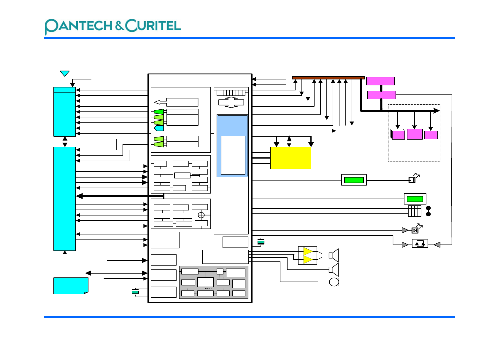
2.2.2 Block Diagram (LOGIC Part)
PAM
RF
and
IF
circuits
IFR
&
RFT
VBAT
T
PA_R1
No use
PA_ON <H >
PA_R0
<H:PAM gain=Low>
LNA_RANGE <H: Hig h G ain>
TRK_LO_ADJ
TX_AGC_ADJ
RX_AGC_ADJ
PLL_CLK, PLL_DATA, PLL_EN <NRZ>
I _OFFSET
Q _OFFSET
SYNTH_LOCK <H: PLL Lock>
CHIPX8 <C lock: 9.8304MHz>
TX_CLK, TX_CLK/
C_RX_IDATA[3:0] <NRZ, 9.8304MHz rate>
C_RX_QDATA[3:0] <NRZ, 9.8304MHz rate>
SLE E P/, IDLE /, FM / < L : Non Native>
TCXO <Clock: 19.2MHz>
ADC_ENAB LE <NR Z>
ADC_CLK <NRZ, Typ 410KHz>
ADC_DATA <NRZ>
<PDM>
<PDM>
<PDM>
<PDM>
<PDM>
/ <Clock, CDM A :4 .9 15 2 M , FM:120 K >
LNA_TX_STATE
TCXO/4
LOCK_DET
TX_DATA
ADC_MU X_1,0
Interface
Digital Control Block
FM/CDMA Freq Track
MUX
MUX
FM/CDMA Tx AGC Loop
MUX
FM/CDMA Rx AGC Loop
PDM
MUX
FM/CDMA I_Offset Loop
MUX
FM/CDMA Q _ O ffset Loop
CDMA Processor
RX부
Searcher
RX부
Demodulator
AD C Interfa c e
Engine
Demodulating
Finger
Com bin in g
block
Frame
Interlea v e r
DFM Processor
2:1
Decimation
WBD Timing
Recovery
General
Purpose
Convolutional
BCH Decode
MSM 5100
Mobile Station Modem
RF
ARM7TDMI
Processor
Subsystem
interface
General
Purpose
Inter fa c e
Encoder
Long Code
PN Gen.
Viterbi
Decoder
Msg. Decode
Word Sync
TX부
Interlea v e r
Walsh code
Modulator
Pilot P N
Generator
LPF
FIR Filter
TX부
1:8
Interpolator
WBD Gen.
UART
Micro
Memory
Sleep-OSC
RESIN/<L:Reset>
W_DOG=H, NMI=L
DP_TX_DATA <NRZ>
DP_RX_DATA <NRZ>
CTS/ <L: Active, N R Z >
RFR/ <L:Active, N R Z >
RI <L: Active , NRZ>
DTR/ <L:Active,NRZ >
DCD <L:A ctive , N R Z >
PS_HOLD <H:Ho ld> , AUD_EN <H:Enable>
AD[0 :15]
RD/
LWR/
ROM
CS/
CAMERA_CS/ <L:Enable>, LENS_PWR_DN/ <L:Enable>,
LCD_CS1/(Main), LCD _CS2/(Sub)
KEYSENSE[0:3] < N RZ, In p u t>
KYPD[09,11,13,15,17] <NRZ, Outpu t>
KEY_LCD_ON <H:Enable>
PWR_LED1 <H:Enable, Green>,
32.768KHz
MCP
LRS1826A
Flash : 128Mbit
SRAM : 32Mbit
CAR_KIT Connector
AD[0:19]
<L:Enable>, LCD_SER_CLK <NRZ>, LCD_SER_IDATA <NRZ>
PWR_LED2 <H:Enable, RED>
Audio AMP
AUX_PCM_SYNC
AUX_PCM_DOUT
AUX_PCM_DIN
Carkit
CHARGER_IC
VBATT
LDO
MPU
AUDIO
(4)
+3V_RX
+3V_R FT_A
+2.85V _D
+3V_A
300K CMO S
CAMERA Module
Main : 128x160dot 65K Color 1.8"
Sub : 96X64 dot B/W CSTN
1 2 3 S
4 5 6 P
7 8 9 M
*
Key Matrix
AMP
LCD
0 # E
PAM
SIDE KEY
Backlight LED
REDGreen
ADC_IN
Note:
• PDM: 0.6 ~ 2.2Volts
• NRZ: 0.4 ~ 3Volts
MODE[2:0] <Not Used>
TCK, TDI, TDO, TMS <Not Used>
TRST/ <Native, L: Reset>
48MHz
Resonator
MODE
SELECT
JTAG
INTERFAC E
USB
QCELP
En/Decoder
SAT
Transpon
d
Deviation
Limiter
Vocoder
DTMF
Generation
& Detect
2:5/5:2
Interpo la to r
CODEC
VOX
Com-
pandor
Pre/De-
Emphasis
14 Tap Tx
Compensation
Filter
u-Law,
A-Law to
Linear
PCM
Sampling
SPK
EAR
MIC
Copyrights 2004 ⓒ Pantech & CuritelZ720i

2.2.3 Block Diagram (POWER PART)
V_PWR (V_BATT)
ON_SW_SEN/
PS_HOLD
SLEEP/ IDLE/ RFU_PWR
MIC5219(U100) MIC5205(U120) MIC5205(U110) MIC5219(U130)
2.85D
2.85D
3.0V_A
Charger IC
MSM5100
IFR3500
RFT3100
2.85V_MSMP
2.85V_MSMA
2.85V_MSMC
3.0V_RX
3.0V_RFT_A
2.85V_TCXO
2.85V_IFR_A
2.85V_IFR_A
PLL
Module
Buffer
AMP
3.0V_RFT_A
V_PWR
LNA
+
PAM
Mixer
TEMP_SEN
TCXO
BL_LED
MSM5100
USB
Audio
AMP
LCD
Folder
Sensor
Vibrator
UIM
Copyrights 2004 ⓒ Pantech & CuritelZ720i

2.3 One Point Fix (Top)
Copyrights 2004 ⓒ Pantech & CuritelZ720i

2.3 One Point Fix (Bottom)
Copyrights 2004 ⓒ Pantech & CuritelZ720i

2.4 New Function
■ Camera Function Block Diagram
CL703S2(Camera Application Processor)
MSM5100
Camera Sensor
Control Data
Data BUS
Control Data
Frame
Buffer
Modem
CPU
Interface
CCD/CIS
Interface
&
Control
Strip
Buffer
JPEG
CODEC
Memory
Controller
System
Controller
YCbCr to
RGB
Converter
LCD/OSD
Interface
SUB LCD
Data BUS
Main LCD
Control DataData BUS
Copyrights 2004 ⓒ Pantech & CuritelZ720i

2.5 New Parts Introduction
■ MSM5100
MSM5100 Device Features
¾ Integrated Universal Serial Bus(USB) interface
¾ Integrated gpsOne Processor for direct interface to
RF chipset
¾ Integrated R-UIM Controller for direct interface to
R-UIM card
¾ Supported IS-2000 1x MC RTT Feature
¾ TCXO : 19.2MHz
¾ Qtunes MP3 player software
¾ Supports peak rates of 153.6kbps on forward link and
reverse link simultaneously
Copyrights 2004 ⓒ Pantech & CuritelZ720i

2.5 New Parts Introduction
■ ITM1010
ITM1010 Device Features
¾ 2.5mm X 2.5mm CDMA receiver Chip
¾ Operating frequency :
CDMA Cellular : 869 ~ 894 MHz
CDMA450 : 460 ~ 470 MHz
¾ High linearity and high gain
¾ Two step LNA gain control
¾ Integrated LNA and down-converter
Copyrights 2004 ⓒ Pantech & CuritelZ720i

2.5 New Parts Introduction
■ IFR3500
IFR3500 Device Features
¾ Including IF AGC AMP, quadrature down –
conversion to analog baseband
¾ Provides receiver functions for two different
operation mode : CDMA and GPS
¾ Removing all FM circuit, TCXO divider/output
buffer circuit
¾ Making the IF LO frequency divider programmable
(2,3,4, or 6)
Copyrights 2004 ⓒ Pantech & CuritelZ720i
2.5 New Parts Introduction
■ RFT3100
RFT3100 Device Features
¾ Connects directly with MSM5100 utilizing an analog
baseband interface
¾ Including IF mixer for upconverting analog
baseband to IF, programmable PLL for generating
TX IF frequency
¾ Including two Cellular and two PCS driver AMP and
TX power control through an 85dB VGA
Copyrights 2004 ⓒ Pantech & CuritelZ720i

2.6 Trouble Shooting Guide
■ No Service 1
Check gain of Duplexer
(F210)(about –3dB)
No
1.Check state of solder Matching
Parts
2.Replace RX RF Saw filter
TP2
YES YES
1,Check power line 3.0V_RX
2.Check In/Output line of LNA
3.TP1 : High TP2 : High
Check Gain of LNA
(about +17dB)
No
Check gain of Mixer
(About +8dB)
No
1.Check power line 3.0V_RX
2.Check IF signal(85.38MHz) at
TP4 and RX_LO signal at TP3
No Signal(85.38MHz)
See Next page No Service2
TP4
TP3
TP1
TP2
TP4
TP1
TP3
Copyrights 2004 ⓒ Pantech & CuritelZ720i

2.6 Trouble Shooting Guide
■ No Service 2
Check RF_LO signal
(Locked) at TP1
No No
1.Check power line 3.0v_RX of PLL
Module
2.Check PLL DATA,CLK,EN
3.Check OCS_in(19.2MHz) Pin of PLL
Module
4. Replace PLL_Module U630
YES YES
Check RF_LO signal
(Locked) at TP2
See Next Page
No Service3
1.Replace Coupler U750
TP2
TP1
TP1
TP2
Copyrights 2004 ⓒ Pantech & CuritelZ720i

2.6 Trouble Shooting Guide
■ No Service 3
Check RX_IF_TANK 170.76MHz at TP1
No
1.Check Voltage of TP2(about 1.4V~1.6V)
2.Check state of Solder RX_IF_TANK Circuit
3.Check Voltage of TP3(about 2.8V)
4.Replace IFR3500
TP2
TP1
TP1
TP3
TP3
Copyrights 2004 ⓒ Pantech & CuritelZ720i
2.6 Trouble Shooting Guide
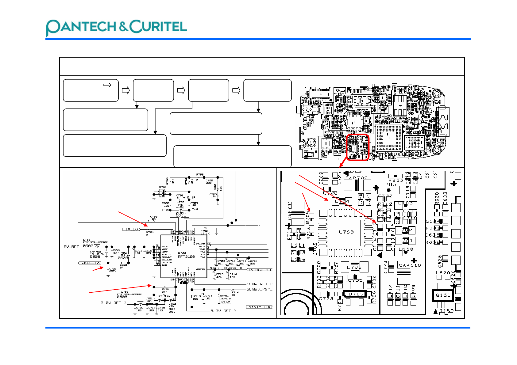
■ No RF TX Power1
After Locking,
##2774+short CAL
+2(TX enable Mode)
Check IDLE/ Signal and output
3.0V_RFT of TX LDO(U110)
1.Check RF_LO signal of PLL_Module
2.Check output of TX_LO Buffer
Amp(U760)
YES YES YES
Check power
line 3.0V_RFT
No
TP1
Check TX_LO
Signal at TP1
1.Check TX_IF_TANK circuit
(190.76MHz)
No
2.Check voltage of TX_AGC_ADJ
1.Check matching parts and RF signal of
RFT3100 at TP3
2.See next page No RF TX Power2
Check IF Signal
95.38MHz at TP2
NO
NO
TP2
TP3
TP1
TP3
TP2
Copyrights 2004 ⓒ Pantech & CuritelZ720i

2.6 Trouble Shooting Guide
■ No RF TX Power2
After Locking,
##2774+short CAL
+2(TX enable Mode)
1.Check PA_ON signal
2.Check R256, C254
3.Replace Load_S/W(U270)
YES YES YES
Check RF
signal at TP1
No
TP2
Check voltage
(About3.7v~4V)
at TP2
1.Check voltage of PAM Vref
(about 3.0V)
2.Replace PAM(U250)
3.Check gain of Saw filter
(FIL250)(about –3dB)
Check gain of
PAM(about +28dB)
No
TP2
TP1
TP1
Copyrights 2004 ⓒ Pantech & CuritelZ720i
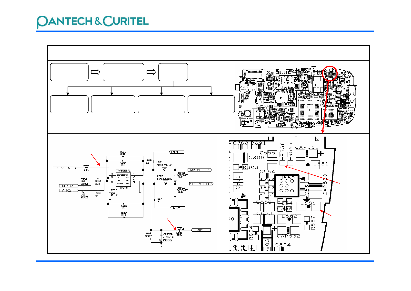
2.6 Trouble Shooting Guide
■ Not work Bell Sound
##1122+END
“1”
YES YESYES
Replace
SPK(Receiver
)
YES YES
Amp(U550)
TP1
Check
SPK(Receiver)
Replace
Audio
TP1:HIGH
TP2:VDC
Check state of
Solder L561,L562
NO
Check state of
Solder R556,L551
TP1
TP2
TP2
Copyrights 2004 ⓒ Pantech & CuritelZ720i