

CDIL SA 1162 Datasheet
Q
Q
Continental Device India Limited
An IS/ISO 9002 and IECQ Certified Manufacturer
Lic#
IS/ISO 9002
SC/L- 000019 .2
IS / IECQC 700000
C 750100
IS / IEC
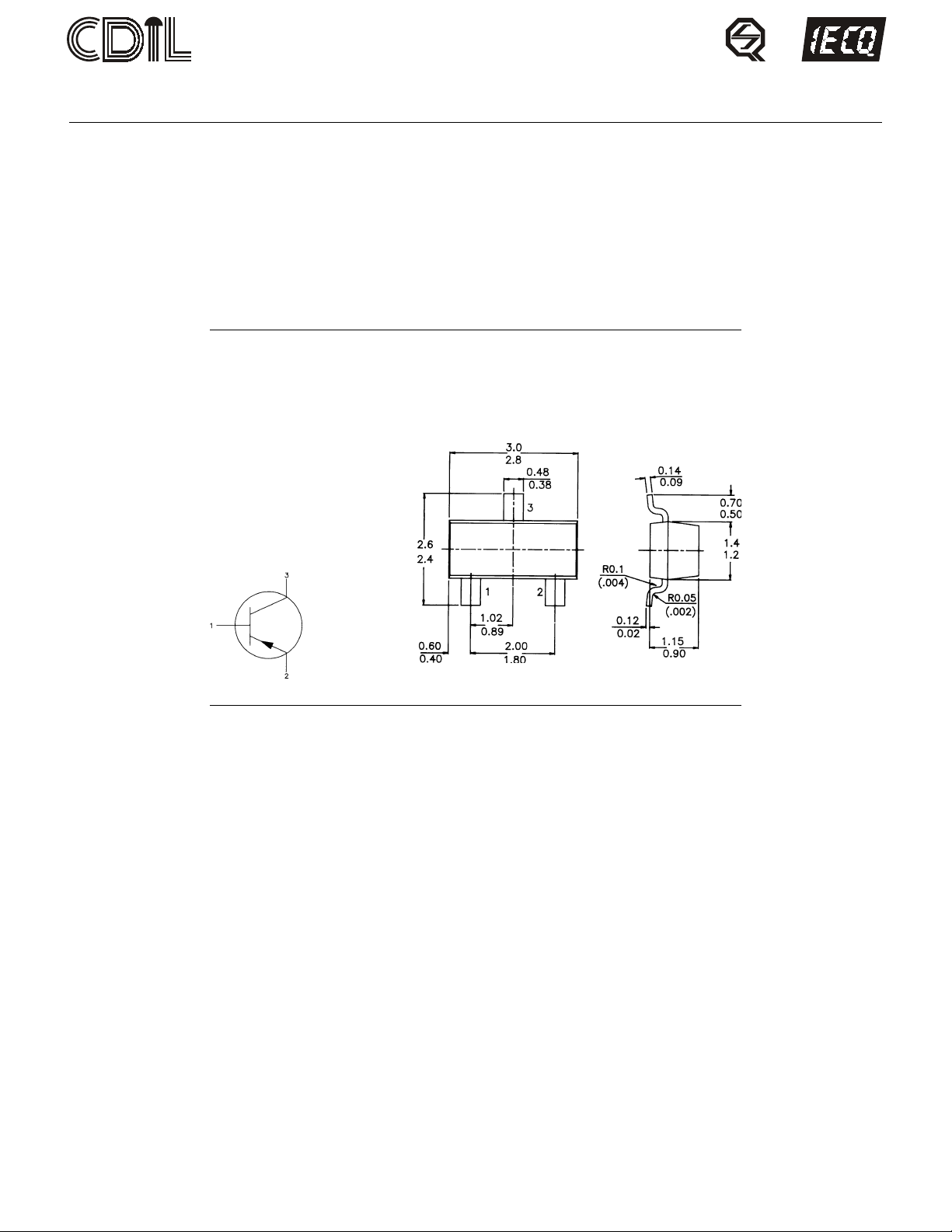
SOT-23 Formed SMD Package
CSA1162
LOW FREQUENCY GENERAL PURPOSE AMPLIFIER TRANSISTOR
P-N-P transistor
Marking
CSA1162Y–3E
CSA1162GR(G)–3F
Pin configuration
1 = BASE
2 = EMITTER
3 = COLLECTOR
PACKAGE OUTLINE DETAILS
ALL DIMENSIONS IN mm
ABSOLUTE MAXIMUM RATINGS
Collector-base voltage (open emitter) –V
Collector-emitter voltage (open base) –V
Emitter-base voltage (open collector) –V
Collector current (d.c.) –I
Total power dissipation at T
= 25°C P
amb
Junction temperature T
D.C. current gain
= 2 mA; –VCE = 6V h
–I
C
RATINGS (at T
= 25°C unless otherwise specified)
A
Limiting values
Collector-base voltage (open emitter) –V
Collector-emitter voltage (open base) –V
Emitter-base voltage (open collector) –V
Collector current (d.c.) –I
Base current –I
tot
j
FE
CBO
CEO
EBO
C
CBO
CEO
EBO
C
B
max. 50 V
max. 50 V
max. 5 V
max. 150 mA
max. 150 mW
max. 150 ° C
min. 70
max. 400
max. 50 V
max. 50 V
max. 5 V
max. 150 mA
max. 30 mA
Continental Device India Limited Data Sheet Page 1 of 2

CSA1162
Total power dissipation at T
= 25°C P
amb
tot
max. 150 mW
Storage temperature Tstg –50 to +150 ° C
Junction temperature T
CHARACTERISTICS (at T
= 25°C unless otherwise specified)
A
j
max. 150 ° C
Collector-emitter breakdown voltage
= 1 mA; IB = 0 –V
–I
C
(BR)CEO
min 50 V
Collector cut-off current
= 50 V; IE = 0 –I
–V
CB
CBO
max. 100 nA
Emitter cut-off current
= 5 V; IC = 0 I
V
EB
EBO
max. 100 nA
Saturation voltage
= 100 mA; –IB = 10 mA –V
–I
C
CEsat
max. 0.3 V
D.C. current gain
= 2 mA; –VCE = 6 V h
I
C
FE
min. 70
max. 400
Y min. 120
max. 240
GR(G) min. 200
max. 400
Transition frequency
= 10 V; IC = 1 mA f
V
CE
Collector output capacitance
= 10 V; IE = 0; f = 1 MHz C
V
CB
Noise figure
= 6 V; IC = 0.1 mA
V
CE
f = 1 kHz; R
= 10 kW N
g
T
ob
F
min. 80 MHz
max. 7 pF
max. 10 dB
Continental Device India Limited Data Sheet Page 2 of 2
 Loading...