

CDIL BF 820 SMD, BF822 SMD Datasheet
Continental Device India Limited
An ISO/TS 16949, ISO 9001 and ISO 14001 Certified Company
SOT-23 Formed SMD Package
SILICON EPITAXIAL TRANSISTORS
N–P–N transistors
Marking
BF820 = 1V
BF822 = 1X
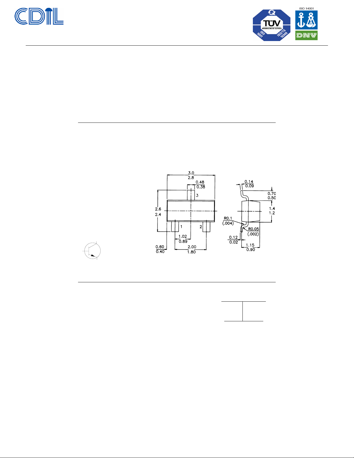
Pin configuration
1 = BASE
2 = EMITTER
3 = COLLECTOR
BF820
BF822
PACKAGE OUTLINE DETAILS
ALL DIMENSIONS IN mm
3
1
2
ABSOLUTE MAXIMUM RATINGS
Collector–base voltage (open emitter) V
Collector–emitter voltage (open base) V
Collector–emitter voltage (R
= 2,7 kW )V
BE
Collector current (peak value) I
Total power dissipation up to T
= 25 °C P
amb
Junction temperature T
D.C. current gain
= 25 mA; VCE = 20 V h
I
C
Feedback capacitance at f = 1 MHz
= 0; VCE = 30 V C
I
C
Transition frequency at f = 35 MHz
= 10mA; VCE = 10 V f
I
C
BF820 BF822
max. 300 250 V
CB0
max. – 250 V
CE0
max. 300 — V
CER
max. 100 mA
CM
max. 250 mW
tot
max. 150 ° C
j
>50
FE
< 1,6 pF
re
>60
T
MHz
Continental Device India Limited Data Sheet Page 1 of 3

BF820
BF822
RATINGS (at TA = 25°C unless otherwise specified)
Limiting values
BF820 BF822
Collector–base voltage (open emitter) V
Collector–emitter voltage (open base) V
Collector–emitter voltage (R
= 2,7 kW )V
BE
Emitter–base voltage (open collector) V
Collector current (d.c.) I
Collector current (peak value) I
Total power dissipation
up to T
= 25 °C P
amb
Storage temperature T
Junction temperature T
THERMAL RESISTANCE
From junction to ambient R
CHARACTERISTICS BF820 BF822
Tj = 25 °C unless otherwise specified
Collector cut–off current
= 0; VCB = 200 V I
I
E
Collector–emitter voltage
= 2,7 kW ; VCE = 250 V I
R
BE
= 2,7kW ; VCE = 200V; Tj = 150°C I
R
BE
Saturation voltage
= 30 mA; lB = 5 mA V
I
C
D.C. current gain
= 25 mA; VCE = 20 V h
I
C
Transition frequency at f
= 10 mA; VCE = 10 V f
l
C
=
35 MHz
Feedback capacitance at f = 1 MHz
= 0; VCE = 30 V C
I
C
max. 300 250 V
CB0
max. – 250 V
CE0
max. 300 — V
CER
max. 5 V
EB0
max. 50 mA
C
max. 100 mA
CM
max. 250 mW
tot
stg
max. 150 ° C
j
th j–a
<10 10nA
CB0
<50 50nA
CER
<10 10mA
CER
< 0,6 V
CEsat
>50
FE
>60
T
< 1,6 pF
re
–55 to +150 ° C
500
K/W
MHz
Continental Device India Limited Data Sheet Page 2 of 3
 Loading...