


Inchange Semiconductor Product Specification
固电半导体
INCHANGE SEMICONDUCTOR
Silicon PNP Power Transistors BD910 BD912
DESCRIPTION ·
·With TO-220C package
·Complement to type BD909 BD911
APPLICATIONS
·Intented for use in power linear
and switching applications
PINNING
PIN DESCRIPTION
1
2
3 Base
Emitter
Collector;connected to
mounting base
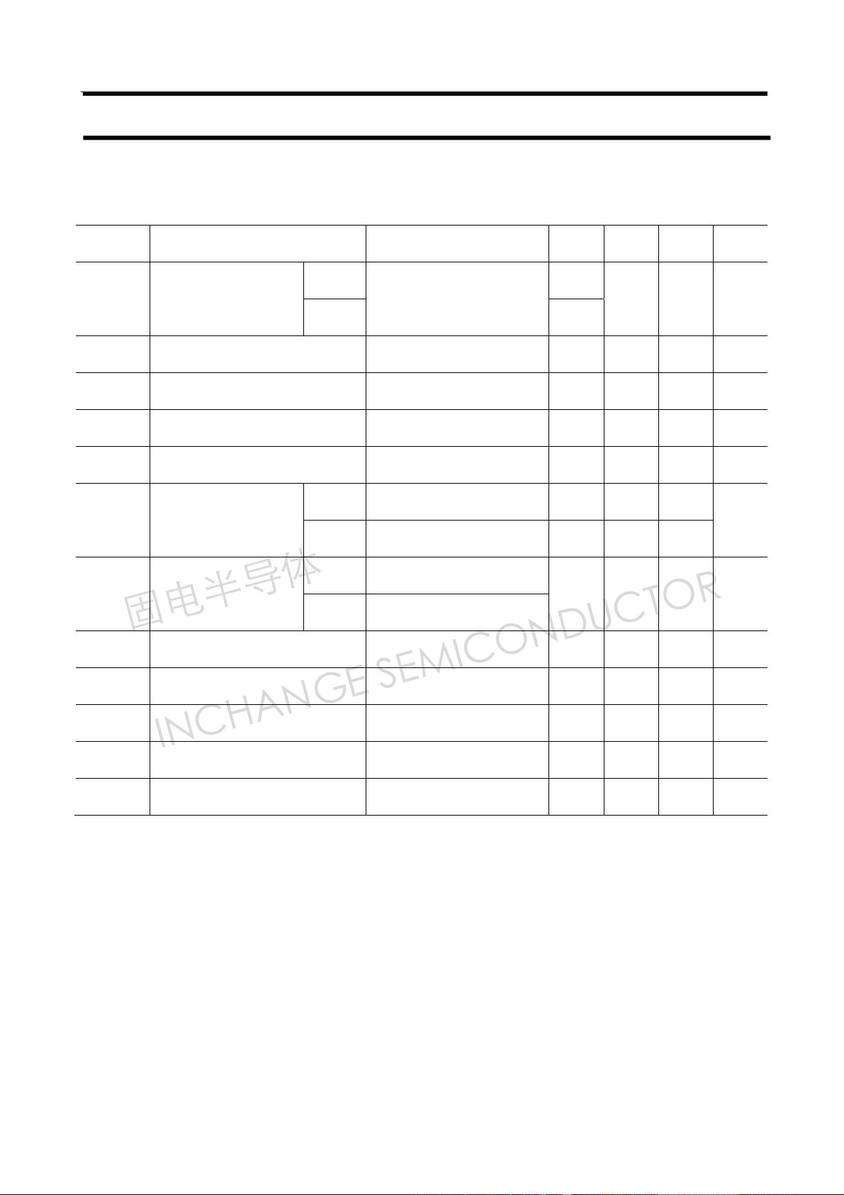
Absolute maximum ratings (Ta=25
SYMBOL PARAMETER CONDITIONS VALUE UNIT
V
CBO
V
CEO
V
EBO
IC Collector current -15 A
IB Base current -5 A
PC Collector power dissipation
Collector-base voltage
Collector-emitter voltage
Emitter-base voltage Open collector -5 V
℃)
BD910 -80
Open emitter
BD912
BD910 -80
Open base
BD912
T
≤25℃
C
-100
-100
90 W
V
V
Tj Junction temperature 150
T
Storage temperature -65~150
stg
THERMAL CHARACTERISTICS
SYMBOL PARAMETER MAX UNIT
R
Thermal resistance junction to case 1.4
th j-c
℃
℃
℃/W
Inchange Semiconductor Product Specification
固电半导体
INCHANGE SEMICONDUCTOR
Silicon PNP Power Transistors BD910 BD912
CHARACTERISTICS
Tj=25℃ unless otherwise specified
SYMBOL PARAMETER CONDITIONS MIN TYP. MAX UNIT
V
CEO(SUS)
V
CEsat-1
V
CEsat-2
V
BEsat
V
BE
I
CBO
I
CEO
I
EBO
h
FE-1
Collector-emitter
sustaining voltage
Collector-emitter saturation voltage IC=-5 A;IB=-0.5 A -1.0 V
Collector-emitter saturation voltage IC=-10A;IB=-2.5 A -3.0 V
Base-emitter saturation voltage IC=-10A;IB=-2.5 A -2.5 V
Base-emitter voltage IC=-5A ; VCE=-4V -1.5 V
Collector cut-off current
Collector cut-off current
Emitter cut-off current VEB=-5V; IC=0 -1.0 mA
DC current gain IC=-0.5A ; VCE=-4V 40 250
BD910 -80
IC=-0.1A; IB=0
BD912
V
=-80V; IE=0
BD910
BD912
BD910 VCE=-40V; IB=0
BD912 V
CB
=150℃
T
C
V
=-100V; IE=0
CB
TC=150℃
=-50V; IB=0
CE
-100
-1.0 mA
V
-0.5
-5.0
-0.5
-5.0
mA
h
DC current gain IC=-5A ; VCE=-4V 15 150
FE-2
h
DC current gain IC=-10A ; VCE=-4V 5
FE-3
fT Transition frequency IC=-0.5A ; VCE=-4V 3 MHz
2
 Loading...