

CDIL BCX 70H SMD Datasheet

NPN Silicon AF Transistors
• For AF input stages and driver applications
• High current gain
• Low collector-emitter saturation voltage
• Low noise between 30 Hz and 15 kHz
• Complementary types: BCW61, BCX71 (PNP)
• Pb-free (RoHS compliant) package
• Qualified according AEC Q101
1)
BCW60, BCX70
3
2
1
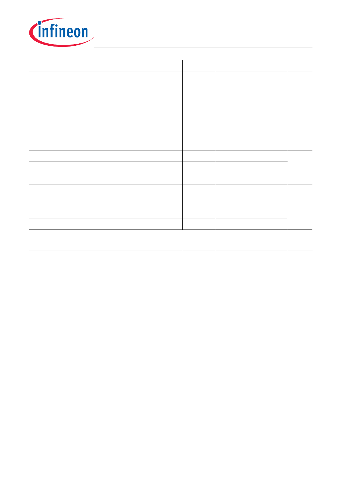
Type Marking Pin Configuration Package
BCW60B
BCW60C
BCW60D
BCW60FF
BCX70G
BCX70H
BCX70J
BCX70K
1
Pb-containing package may be available upon special request
ABs
ACs
ADs
AFs
AGs
AHs
AJs
AKs
1=B
1=B
1=B
1=B
1=B
1=B
1=B
1=B
2=E
2=E
2=E
2=E
2=E
2=E
2=E
2=E
3=C
3=C
3=C
3=C
3=C
3=C
3=C
3=C
SOT23
SOT23
SOT23
SOT23
SOT23
SOT23
SOT23
SOT23
1
2007-04-20
Maximum Ratings
BCW60, BCX70
Parameter
Collector-emitter voltage
Symbol Value Unit
V
BCW60, ...60FF
BCX70
Collector-base voltage
V
BCW60, ...60FF
BCX70
Emitter-base voltage V
Collector current I
Peak collector current I
Peak base current I
Total power dissipation
T
≤ 71 °C
S
P
Junction temperature T
Storage temperature T
CEO
CBO
EBO
C
CM
BM
tot
j
stg
32
45
32
45
6
100 mA
200
200
330 mW
150 °C
-65 ... 150
V
Thermal Resistance
Parameter
Junction - soldering point
1
For calculation of R
please refer to Application Note Thermal Resistance
thJA
1)
Symbol Value Unit
R
thJS
≤ 240
K/W
2
2007-04-20

Electrical Characteristics at TA = 25°C, unless otherwise specified
BCW60, BCX70
Parameter
DC Characteristics
Collector-emitter breakdown voltage
I
= 10 mA, IB = 0 , BCW60, ...60FF
C
I
= 10 mA, IB = 0 , BCX70
C
Collector-base breakdown voltage
I
= 10 µA, IE = 0 , BCW60, ...60FF
C
I
= 10 µA, IE = 0 , BCX70
C
Emitter-base breakdown voltage
I
= 1 µA, IC = 0
E
Collector-base cutoff current
V
= 32 V, IE = 0 , BCW60, ...60FF
CB
V
= 45 V, IE = 0 , BCX70
CB
V
= 32 V, IE = 0 , TA = 150 °C, BCW60, ...60FF
CB
V
= 45 V, IE = 0 , TA = 150 °C, BCX70
CB
Symbol Values Unit
min. typ. max.
V
(BR)CEO
V
(BR)CBO
V
(BR)EBO
I
CBO
32
45
32
45
-
-
-
-
6 - -
-
-
-
-
-
-
-
-
-
-
-
-
0.02
0.02
20
20
V
µA
Emitter-base cutoff current
V
= 4 V, IC = 0
EB
DC current gain-
I
= 10 µA, VCE = 5 V, hFE-grp. G
C
I
= 10 µA, VCE = 5 V, hFE-grp. B/ H
C
I
= 10 µA, VCE = 5 V, hFE-grp. C/ J/ FF
C
I
= 10 µA, VCE = 5 V, hFE-grp. D/ K
C
I
= 2 mA, VCE = 5 V, hFE-grp. G
C
I
= 2 mA, VCE = 5 V, hFE-grp. B/ H
C
I
= 2 mA, VCE = 5 V, hFE-grp. C/ J/ FF
C
I
= 2 mA, VCE = 5 V, hFE-grp. D/ K
C
I
= 50 mA, VCE = 1 V, hFE-grp. G
C
I
= 50 mA, VCE = 1 V, hFE-grp. B/ H
C
I
= 50 mA, VCE = 1 V, hFE-grp. C/ J/ FF
C
I
= 50 mA, VCE = 1 V, hFE-grp. D/ K
C
I
EBO
h
FE
- - 20 nA
20
20
40
100
120
180
250
380
50
70
90
100
140
200
300
460
170
250
350
500
-
-
-
-
-
-
-
-
220
310
460
630
-
-
-
-
-
3
2007-04-20

DC Electrical Characteristics
BCW60, BCX70
Parameter
Characteristics
Collector-emitter saturation voltage1)
I
= 10 mA, IB = 0.25 mA
C
I
= 50 mA, IB = 1.25 mA
C
Base emitter saturation voltage1)
I
= 10 mA, IB = 0.25 mA
C
I
= 50 mA, IB = 1.25 mA
C
Base-emitter voltage1)
I
= 10 µA, VCE = 5 V
C
I
= 2 mA, VCE = 5 V
C
I
= 50 mA, VCE = 1 V
C
1
Pulse test: t < 300µs; D < 2%
Symbol Values Unit
min. typ. max.
V
CEsat
V
BEsat
V
BE(ON)
-
-
-
-
-
0.58
-
0.12
0.2
0.7
0.83
0.52
0.65
0.78
0.25
0.55
0.85
1.05
0.7
V
-
-
4
2007-04-20
 Loading...