CDIDI 1N5546B, 1N5545B, 1N5544B, 1N5543B, 1N5542B Datasheet
...
22 COREY STREET, MELROSE, MASSACHUSETTS 02176
PHONE (781) 665-1071 FAX (781) 665-7379
WEBSITE: http://www.cdi-diodes.com E-mail: mail@cdi-diodes.com
MAXIMUM RATINGS
Junction and Storage Temperature: -65°C to +175°C
DC Power Dissipation: 500 mW @ +50°C
Power Derating: 4 mW / °C above +50°C
Forward Voltage @ 200mA: 1.1 volts maximum
ELECTRICAL CHARACTERISTICS @ 25°C
B-C-D
SUFFIX B-C-D SUFFIX
JEDEC NOMINAL ZENER MAX. ZENER MAXIMUM REVERSE MAXIMUM MAX. NOISE REGULATION LOW
TYPE ZENER TEST IMPEDANCE LEAKAGE CURRENT DC ZENER DENSITY FACTOR V
Z
NUMBER VOLTAGE CURRENT B-C-D SUFFIX CURRENT @1
Z=250
µ
A
CURRENT
VZ@ 1
ZT1ZTZZT
@ 1
ZT
l
R
VR= VOLTS 1
ZM
N
D
∆V
Z
1
ZL
(NOTE 1) (NOTE 2) (NOTE 3) (NOTE 4) (NOTE 5)
NON & A- B-C-D-
VOLTS mAdc OHMS
µ
Adc SUFFIX SUFFIX mAdc
µ
V/ HZ VOLTS mAdc
1N5518B 3.3 20 26 5.0 0.90 1.0 115 0.5 0.90 2.0
1N5519B 3.6 20 24 3.0 0.90 1.0 105 0.5 0.90 2.0
1N5520B 3.9 20 22 1.0 0.90 1.0 98 0.5 0.85 2.0
1N5521B 4.3 20 18 3.0 1.0 1.5 88 0.5 0.75 2.0
1N5522B 4.7 10 22 2.0 1.5 2.0 81 0.5 0.60 1.0
1N5523B 5.1 5.0 26 2.0 2.0 2.5 75 0.5 0.65 0.25
1N5524B 5.6 3.0 30 2.0 3.0 3.5 68 1.0 0.30 0.25
1N5525B 6.2 1.0 30 1.0 4.5 5.0 61 1.0 0.20 0.01
1N5526B 6.8 1.0 30 1.0 5.5 6.2 56 1.0 0.10 0.01
1N5527B 7.5 1.0 35 0.5 6.0 6.8 51 2.0 0.05 0.01
1N5528B 8.2 1.0 40 0.5 6.5 7.5 46 4.0 0.05 0.01
1N5529B 9.1 1.0 45 0.1 7.0 8.2 42 4.0 0.05 0.01
1N5530B 10.0 1.0 60 0.05 8.0 9.1 38 4.0 0.10 0.01
1N5531B 11.0 1.0 80 0.05 9.0 9.9 35 5.0 0.20 0.01
1N5532B 12.0 1.0 90 0.05 9.5 10.8 32 10 0.20 0.01
1N5533B 13.0 1.0 90 0.01 10.5 11.7 29 15 0.20 0.01
1N5534B 14.0 1.0 100 0.01 11.5 12.6 27 20 0.20 0.01
1N5535B 15.0 1.0 100 0.01 12.5 13.5 25 20 0.20 0.01
1N5536B 16.0 1.0 100 0.01 13.0 14.4 24 20 0.20 0.01
1N5537B 17.0 1.0 100 0.01 14.0 15.3 22 20 0.20 0.01
1N5538B 18.0 1.0 100 0.01 15.0 16.2 21 20 0.20 0.01
1N5539B 19.0 1.0 100 0.01 16.0 17.1 20 20 0.20 0.01
1N5540B 20.0 1.0 100 0.01 17.0 18.0 19 20 0.20 0.01
1N5541B 22.0 1.0 100 0.01 18.0 19.8 17 20 0.25 0.01
1N5542B 24.0 1.0 100 0.01 20.0 21.6 16 20 0.30 0.01
1N5543B 25.0 1.0 100 0.01 21.0 22.4 15 20 0.35 0.01
1N5544B 28.0 1.0 100 0.01 23.0 25.2 14 20 0.40 0.01
1N5545B 30.0 1.0 100 0.01 24.0 27.0 13 20 0.45 0.01
1N5546B 33.0 1.0 100 0.01 28.0 29.7 12 20 0.50 0.01
NOTE 1 No Suffix type numbers are +20% with guaranteed limits for only V
Z
, lR, and VF. Units
with “A” suffix are +
10% with guaranteed limits for VZ, lR, and VF. Units with guaranteed limits for
all six parameters are indicated by a “B” suffix for +
5.0% units, “C” suffix for +2.0% and “D” suffix
for +
1.0%.
NOTE 2 Zener voltage is measured with the device junction in thermal equilibrium at an ambient
temperature of 25°C +
3°C.
NOTE 3 Zener impedance is derived by superimposing on 1
ZT
A 60Hz rms a.c. current equal to 10% of 1
ZT.
NOTE 4 Reverse leakage currents are measured at VRas shown on the table.
NOTE 5 ∆VZ is the maximum difference between VZ at lZT and VZat lZLmeasured with
the device junction in thermal equilibrium at the ambient temperature of +25°C +
3°C.
DESIGN DATA
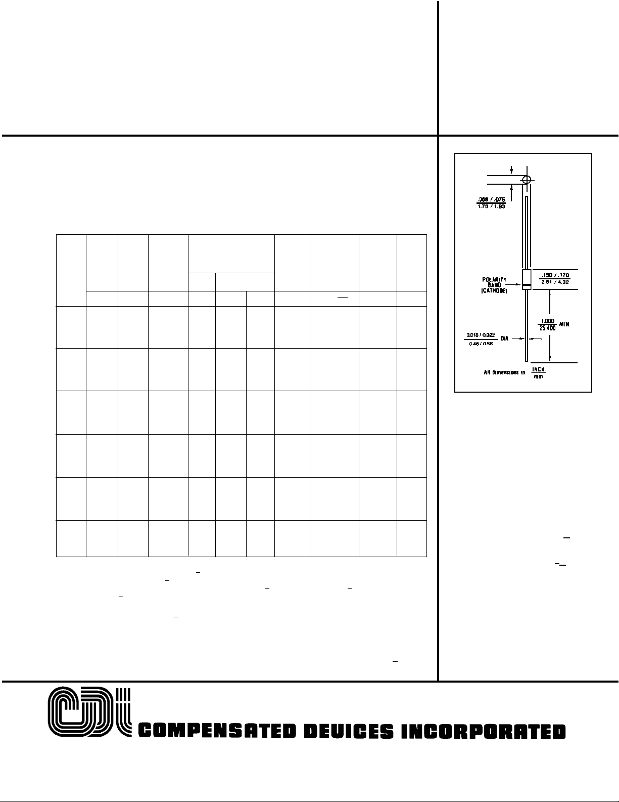
CASE: Hermetically sealed glass
case. DO – 35 outline.
LEAD MATERIAL: Copper clad steel.
LEAD FINISH: Tin / Lead
THERMAL RESISTANCE: (R
O
JEC
):
250 ˚C/W maximum at L = .375 inch
THERMAL IMPEDANCE: (Z
OJX
): 35
˚C/W maximum
POLARITY: Diode to be operated with
the banded (cathode) end positive.
MOUNTING POSITION: Any.
FIGURE 1
• 1N5518-1 THRU 1N5546B-1 AVAILABLE IN
JAN, JANTX AND JANTXV
PER MIL-PRF-19500/437
• LOW REVERSE LEAKAGE CHARACTERISTICS
• LOW NOISE CHARACTERISTICS
• DOUBLE PLUG CONSTRUCTION
• METALLURGICALLY BONDED
1N5518 thru 1N5546D
and
1N5518B-1 thru 1N5546B-1
√

1N5518 thru 1N5546D
INCLUDING -1 VERSIONS
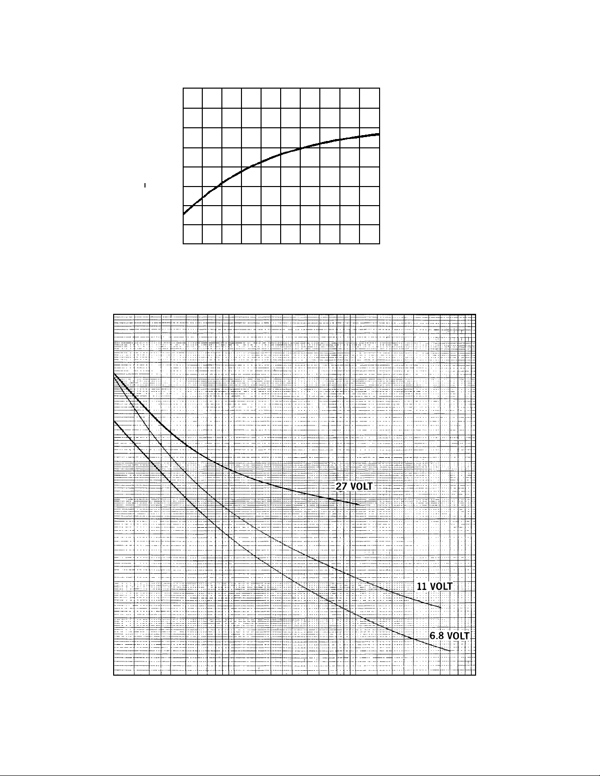
.1 .2 .5 1 2 5 10 20 50 100
OPERATING CURRENT I
ZT (mA)
FIGURE 3
ZENER IMPEDANCE VS. OPERATING CURRENT
ZENER IMPEDANCE ZZT (OHMS)
1000
500
400
300
200
100
50
40
30
20
10
5
4
3
2
1
400
300
200
100
0JL, Junction to Lead
Thermal Resistance (°C/W)
0 0.2 0.4 0.6 0.8 1.0
L, lead Length to Heat Sink (inches)
FIGURE 2
TYPICAL THERMAL RESISTANCE
 Loading...