

Page 1
5
4
3
2
1
Topstar Digital technologies Co.,LTD
D D
Board name: Mother Board Schematic
Project name: X03
Version: Ver A
Initial Date:
1. System Block Diagram & Schematic page description;
2. Power Block Diagram & Discription;
3. Annotations & information;
4. Schematic modify Item and history;
New update: 5. Power on & off Sequence;
6. ACPI Mode Switch Timings;
7. Power On Sequence Map;
8. CLOCK Distribution;
C C
9. Power Distribution;
Topstar Confidential
Hardware drawing by:
Power drawing by:
B B
Hardware check by: EMI Check by:
Power check by:
Manager Sign by:
A A
Page Name
Page Name
Page Name
Size
Size
Size
Project Name Rev
Project Name Rev
Project Name Rev
A3
A3
A3
Date: Sheet
Date: Sheet
Date: Sheet
PROPERTY NOTE: this document contains information confidential and property to
PROPERTY NOTE: this document contains information confidential and property to
PROPERTY NOTE: this document contains information confidential and property to
TOPSTAR and shall not be reproduced or transferred to other documents or disclosed
TOPSTAR and shall not be reproduced or transferred to other documents or disclosed
TOPSTAR and shall not be reproduced or transferred to other documents or disclosed
to others or used for any purpose other than that for which it was obtained without
to others or used for any purpose other than that for which it was obtained without
to others or used for any purpose other than that for which it was obtained without
the expressed written consent of TOPSTAR
the expressed written consent of TOPSTAR
5
4
3
2
the expressed written consent of TOPSTAR
TOPSTAR TECHNOLOGY
TOPSTAR TECHNOLOGY
TOPSTAR TECHNOLOGY
Swain Xu(
Swain Xu(
Swain Xu(
)
)
Title
Title
Title
X03
X03
X03
)
1
A
A
139Thursday, April 29, 2010
139Thursday, April 29, 2010
139Thursday, April 29, 2010
A
of
of
of
Page 2
5
4
3
2
1
CONTENT
Topstar Confidential
ShenZhen Topstar Industry Co.,LTD
D D
P01 SYSTEM BLOCK Ver:A
1 Title
2 System Block & Sch Page
3 PWR Block & description
4 NOTE and Annotations
5 Sch Modify and history
6 CK-505M
7 Pineview Host/k/LVDS/DMI
8 Pineview DDR3
9 Pineview VGA/RVDS
10 Pineview Power
11 CTR CONN
Backlight
Connector
+VDC
PG 15
CK505M
Clocking
CY28548
+V3.3S
PG 6
12 LVDS Inverter CONN
10.1' LED
+V3.3S
LVDS
PG 12
VGA
C C
+V5S
PG 11
R/G/B
Pineview
FCBGA 437PIN
+VCC_CORE,+VCCP
+1.05V,+V0.89V,+V1.8V
PG 7,8,9,10
DDR3
667
DDR2 SODIMM0
667
+V0.75S,+V1.5,
PG 13
13 DDRII SODIMM0
14 Tigerpoint (1of3)
15 Tigerpoint (2of3)
16 Tigerpoint (3of3)
17 SATA HDD
18 Card Reader
19 PCIE MINI SLOT 1
20 PCIE MINI SLOT 2
21 USB Port & FAN
22 Audio (ALC662)
23 LED
SIM CARD
PG 20
PCIE mini Card
PG 20
PCIE mini Card
PG 19
DMI x2
Gen1
PCIE X1
10/100M
LAN
RTL8105E
+V3.3AL,+V3.3S
RJ45
PG 26
PCIE 1X
USB1.1/2.0
B B
BIOS
8Mbit
+V3.3AL
PG 25
Tigerpoint
82801GBM 652 BGA
+V1.05S,+V3.3S
+V3.3AL,+V5AL
+V1.5S,+V5S
+V3.3A_RTC
PG 14,15,16
SATAO(R1.0)
S-ATA
2.5" HHD
+V5S,+V3.3S
PG 17
24 OTP
25 KBC(KB3310B)
26 LAN(RTL8105)
27 ADAPTER IN
28 BATTERY JACK
29 V3.3AL/+V5AL POWER
30 DDR V1.8/+V0.9S POWER
31 V1.5S/+V1.05S POWER
32 Power Good Logic_OVP
33 V5S/V3.3S/V1.8S/V1.2 Power
34 VCORE POWER
35 Power Discharge Circuit
36 CHARGER
37 Power On Secquence & Reset M
38 Power ON/OFF
39 Touchpad Board
USB PORT1
+V5AL
PG 21
USB PORT2
+V5AL
CAM
+V5S
A A
SD/MMC/MS/XD CARD
KB Controller/EC
KB3310B
BIOS
8Mbit
+V3.3AL
PG 25
+V3.3AL
PG 25
HDA
KB Matrix
LED & TouchPAD
AMP
TPS6017A2
+V5S
PG 22
AZALIA
ALC662
+V5S,+V3.3S
PG 22
PG 18
5
4
3
Speaker
L
R
MiC
PG 22
Audio Jack
TOPSTAR TECHNOLOGY
TOPSTAR TECHNOLOGY
TOPSTAR TECHNOLOGY
Swain Xu(
1
)
)
)
A
A
239Thursday, April 29, 2010
239Thursday, April 29, 2010
239Thursday, April 29, 2010
A
of
of
of
Swain Xu(
Page Name
Page Name
Page Name
Size
Size
Size
Project Name Rev
Project Name Rev
Project Name Rev
A3
A3
A3
Date: Sheet
Date: Sheet
Date: Sheet
PROPERTY NOTE: this document contains information confidential and property to
PROPERTY NOTE: this document contains information confidential and property to
PROPERTY NOTE: this document contains information confidential and property to
TOPSTAR and shall not be reproduced or transferred to other documents or disclosed
TOPSTAR and shall not be reproduced or transferred to other documents or disclosed
TOPSTAR and shall not be reproduced or transferred to other documents or disclosed
to others or used for any purpose other than that for which it was obtained without
to others or used for any purpose other than that for which it was obtained without
to others or used for any purpose other than that for which it was obtained without
the expressed written consent of TOPSTAR
the expressed written consent of TOPSTAR
2
the expressed written consent of TOPSTAR
Swain Xu(
System Block & Index
System Block & Index
System Block & Index
P01
P01
P01
Page 3
5
4
3
2
1
D D
Charger power
ISL6251
P02H POWER BLOCK Ver:A
Battery
6V-8.4V
4A
C C
B B
Adapter
12V 2.5A
Always power
ISL62382
+V3.3AL,5A
/+V5AL,4A
MOSFET
Switch
Power
Switch
Chipset Power
ISL6545
+V1.05S,4A
+VDC
DDR Power
ISL6545
+V1.8 6A
VCC_CORE
ISL6545
+VCC_CORE
1.1V,6A
GFX Power
ISL6545
+0.89S 3A
+V3.3S,4A
/+V5S,4A
A A
5
4
MOSFET
Switch
+V1.8S 0.5A
LDO
+V1.5S 2A
3
LDO
+V0.9S 2A
TOPSTAR TECHNOLOGY
TOPSTAR TECHNOLOGY
TOPSTAR TECHNOLOGY
Page Name
Page Name
Page Name
Size
Size
Size
Project Name Rev
Project Name Rev
Project Name Rev
A3
A3
A3
Date: Sheet
Date: Sheet
Date: Sheet
PROPERTY NOTE: this document contains information confidential and property to
PROPERTY NOTE: this document contains information confidential and property to
PROPERTY NOTE: this document contains information confidential and property to
TOPSTAR and shall not be reproduced or transferred to other documents or disclosed
TOPSTAR and shall not be reproduced or transferred to other documents or disclosed
TOPSTAR and shall not be reproduced or transferred to other documents or disclosed
to others or used for any purpose other than that for which it was obtained without
to others or used for any purpose other than that for which it was obtained without
to others or used for any purpose other than that for which it was obtained without
the expressed written consent of TOPSTAR
the expressed written consent of TOPSTAR
2
the expressed written consent of TOPSTAR
PWR Block & description
PWR Block & description
PWR Block & description
Swain Xu(
Swain Xu(
Swain Xu(
P01
P01
P01
)
)
)
A
A
339Thursday, April 29, 2010
339Thursday, April 29, 2010
339Thursday, April 29, 2010
1
A
of
of
of
Page 4
5
A
4
3
2
1
Voltage Rails
+VDC
D D
+VBATTERY
+VCC_CORE
+V1.05S
+V1.8
+V0.9S
+V3.3AL
+V5AL
+V3.3S
+V5S
+V0.89S 0.89V power rail for Pineview Graphics core
Primary DC system power supply (6V-9.5V)
Battery Power supply (6-8.4V)
Core Voltage for CPU
1.05V for Calistoga & ICH7M core / FSB VTT
1.8V power rail for DDR2
0.9V DDR2 Termination voltage
3.3V always on power rail
5V for ICH7-M's VCC5 Refsus
3.3V main power rail
5V main power rail
C C
Board stack up description
PCB Layers
Top(Signal1)
VCC 2
Signal 3
Signal4
Ground 5
Bottom(Signal6)
Trace Impedence:55ohm +/-15%
I2C SMB Address
Device
Clock Generator
SO-DIMM0
CPU Thermal Sensor
Smart Battery
PCIE Slot
Power States
Signal
S0(Full On)
S3(STM)
S4(STD)
S5(SoftOff)
SLP_S3#
HIGH
LOW
LOW
LOW
Wake up Events
LID switch from EC
Power switch from EC
Address Hex
1101 001x
1010 000x
1001 100x
0001 011x
TBD
SLP_S4#
D2
A0
98
16
TBD
HIGH
HIGH
LOW
LOW
SLP_S5#
HIGH
HIGH
HIGH
LOW
Master
ICH7-M
ICH7-M
KBC
KBC
ICH7-M
+V*ALW
ON
ON
ON
ON
+V*
ON ON
ON
OFF
OFF
+V*S
OFF
OFF
OFF
Clock
ON
OFF
OFF
OFF
B B
USB Table
USB Port#
0
1
2
3
4
5
6
7
Function Description
Standard USB2.0 Port
Standard USB2.0 Port
Standard USB2.0 Port
MINICARD_USB
CAM_USB
MINICARD_USB
CR_USB
NC
PCB Footprints
3
SOT23
1 2
5
SOT23_5
3
21
4
ns: Component marked "ns" is not stuff
TOPSTAR TECHNOLOGY
TOPSTAR TECHNOLOGY
TOPSTAR TECHNOLOGY
Swain Xu(
Swain Xu(
Swain Xu(
)
)
Page Name
Page Name
Page Name
Size
Size
Size
Project Name Rev
Project Name Rev
Project Name Rev
A3
A3
A3
Date: Sheet
Date: Sheet
Date: Sheet
PROPERTY NOTE: this document contains information confidential and property to
PROPERTY NOTE: this document contains information confidential and property to
PROPERTY NOTE: this document contains information confidential and property to
TOPSTAR and shall not be reproduced or transferred to other documents or disclosed
TOPSTAR and shall not be reproduced or transferred to other documents or disclosed
TOPSTAR and shall not be reproduced or transferred to other documents or disclosed
to others or used for any purpose other than that for which it was obtained without
to others or used for any purpose other than that for which it was obtained without
to others or used for any purpose other than that for which it was obtained without
the expressed written consent of TOPSTAR
the expressed written consent of TOPSTAR
the expressed written consent of TOPSTAR
NOTE
NOTE
NOTE
P01
P01
P01
)
439Thursday, April 29, 2010
439Thursday, April 29, 2010
439Thursday, April 29, 2010
of
of
of
A
A
A
A
Page 5
5
4
3
2
1
Schematic modify Item and history:
P02 VerA Release2009-7-6
P02 VerB
2009-8-21
D D
PG13: Add SM_VREF circuit
PG20: change SIMCARD connector to 621200700002
2009-8-24
PG25: Stuff TPCLK TPDAT pull up resistors
2009-8-27
PG31: Delete 0.89S reserved circuit
PG33: Delete 1.2S reserved circuit
2009-9-7
PG18: change IT1337E power rail to +V3.3AL follow demo
2009-9-8
PG6: Delete Clock Generator SMBUS 0ohm resistors
PG10: Delete 1.8S 1.2S colay circuit,change net name
C C
PG11: Delete reserved 0ohm resistors that connect GND and GND_VGA
PG13: change 2.2uF capacitors from 0805 to 0603 for layout issue
2009-9-9
PG25: Delete keyboard scanin pull up RN
PG25: Delete A20gate RCIN# reserved 2N7002
PG31: Delete colay +V5S
PG35: Delete IMVP_PWRGD reserved circuit
2009-9-14
PG6: change PCI clcok,ICH 14.318MHz clock source resistors from 22ohm
to 33ohm for SI issue
2009-9-15
PG6: change Clock Generator Crystal Y3 to TFL small package for layout issue
PG16: change boardid from vera to verb
B B
PG25: change PCB version to VerB
PG27: Connect JACK_GND with GND
2009-9-17
PG6: BUS Frequence controlled by CPU
P02 VerB Release2009-9-18
P02 VerC
2009-10-23
PG23: ADD MSI wifi/bt 2in1 module connector and peripheral circuit
PG25: ADD MSI wifi/bt 2in1 module 3 control signals to EC gpio
2009-10-26
A A
PG29: delet open points of +V3.3AL and +V5AL
2009-10-27
PG19: change part reference of pcie nut to PCIE_NUT2
2009-10-28
PG25: Colay small package EC
5
Page Name
Page Name
Page Name
Size
Size
Size
Project Name Rev
Project Name Rev
Project Name Rev
A3
A3
A3
Date: Sheet
Date: Sheet
Date: Sheet
PROPERTY NOTE: this document contains information confidential and property to
PROPERTY NOTE: this document contains information confidential and property to
PROPERTY NOTE: this document contains information confidential and property to
TOPSTAR and shall not be reproduced or transferred to other documents or disclosed
TOPSTAR and shall not be reproduced or transferred to other documents or disclosed
TOPSTAR and shall not be reproduced or transferred to other documents or disclosed
to others or used for any purpose other than that for which it was obtained without
to others or used for any purpose other than that for which it was obtained without
to others or used for any purpose other than that for which it was obtained without
the expressed written consent of TOPSTAR
the expressed written consent of TOPSTAR
4
3
2
the expressed written consent of TOPSTAR
TOPSTAR TECHNOLOGY
TOPSTAR TECHNOLOGY
TOPSTAR TECHNOLOGY
Swain Xu(
Swain Xu(
Swain Xu(
Sch Modify and history
Sch Modify and history
Sch Modify and history
P01
P01
P01
1
)
)
)
A
A
539Thursday, April 29, 2010
539Thursday, April 29, 2010
539Thursday, April 29, 2010
A
of
of
of
Page 6
5
+V3.3S
FB7
FB7
100ohm@100MHz,3A
100ohm@100MHz,3A
FB0805
FB0805
1 2
D D
C98
C98
10UF/6.3V,X5R
10UF/6.3V,X5R
C0805
C0805
+V3.3S
FB8
FB8
100ohm@100MHz,3A
100ohm@100MHz,3A
FB0805
FB0805
1 2
C C
B B
C117
C117
0.1uF/10V,X5R
0.1uF/10V,X5R
C0402
C0402
C103
C103
4.7UF/10V,Y5V
4.7UF/10V,Y5V
C0805
C0805
C100
C100
10UF/6.3V,X5R
10UF/6.3V,X5R
C0805
C0805
C99
C99
10UF/6.3V,X5R
10UF/6.3V,X5R
C0805
C0805
ns
ns
C105
C105
10UF/6.3V,X5R
10UF/6.3V,X5R
C0805
C0805
C116
C116
0.1uF/10V,X5R
0.1uF/10V,X5R
C0402
C0402
C119
C119
0.1uF/10V,X5R
0.1uF/10V,X5R
C0402
C0402
C120
C120
0.1uF/10V,X5R
0.1uF/10V,X5R
C0402
C0402
C94
C94
0.1uF/10V,X5R
0.1uF/10V,X5R
C0402
C0402
C95
C95
0.1uF/10V,X5R
0.1uF/10V,X5R
C0402
C0402
+VDDIO_CLK
+VDDIO_CLK
C115
C115
0.1uF/10V,X5R
0.1uF/10V,X5R
C0402
C0402
C118
C118
0.1uF/10V,X5R
0.1uF/10V,X5R
C0402
C0402
C93
C93
0.047uF/16V,X7R
0.047uF/16V,X7R
C0402
C0402
+VDDIO_CLK
+VDDIO_CLK
BUS FREQUENCE SELECT
CPU_BSEL07
CPU_BSEL17
CPU_BSEL27
CLK_BSEL0
CLK_BSEL1
CLK_BSEL2
R271 1K R0402R271 1K R0402
R272 1K R0402R272 1K R0402
R273 1K R0402R273 1K R0402
4
+V3.3S_CK_VDD
C96
C96
0.1uF/10V,X5R
0.1uF/10V,X5R
C0402
C0402
MCH_BSEL0 9
MCH_BSEL1 9
MCH_BSEL2 9
3
change from 22ohm to 33ohm for SI issue 090914
CLK_BSEL0
CLK_BSEL1
CLK_BSEL2
12
R313 33 R0402R313 33 R0402
R312 33 R0402R312 33 R0402
R311 33 R0402R311 33 R0402
R299 10K R0402R299 10K R0402
Set to SRC8
R316 22 R0402R316 22 R0402
R310 22 R0402R310 22 R0402
R304 2.2K R0402R304 2.2K R0402
R384 10K R0402R384 10K R0402
R395 33 R0402R395 33 R0402
CLK_XTAL_IN
Y3
Y3
14.318180MHz
14.318180MHz
XS2_3D3
XS2_3D3
CLK_XTAL_OUT
CK505_CLK_EN#15,35
+V3.3S
PCI_CLK_EC25
PCI_CLK_DEBUG19
PCI_CLK_ICH14
CR_USB4818
CLK_USB4814
CLK_ICH1415
change from 22ohm to 33ohm for SI issue 090914
C303
C303
27pF/50V,NPO
27pF/50V,NPO
C0402
C0402
C301
C301
27pF/50V,NPO
27pF/50V,NPO
C0402
C0402
+V3.3S_CK_VDD
+VDDIO_CLK
+VDDIO_CLK
+VDDIO_CLK
+VDDIO_CLK
TME
27M_SEL
PCIF_ITP_EN
CLK_XTAL_IN
CLK_XTAL_OUT
No more than 500 mil
R139
R139
1K
1K
R0402
R0402
ns
ns
U14
U14
SLG8SP510T
SLG8SP510T
TSSOP64_0D5_6D1
TSSOP64_0D5_6D1
2
VDD_PCI
9
VDD_48
16
VDD_PLL3
61
VDD_REF
39
VDD_SRC
55
VDD_CPU
12
VDD_IO
20
VDD_PLL3_IO
26
VDD_SRC_IO_1
36
VDD_SRC_IO_2
45
VDD_SRC_IO_3
49
VDD_CPU_IO
1
PCI0/OE#_0/2_A
3
PCI1/OE#_1/4_A
4
PCI2/TME
5
PCI3/FSD
6
PCI4/SRC5_SEL
7
PCIF5/ITP_EN
60
XTAL_IN
59
XTAL_OUT
10
USB_48/FSA
57
FSB/TEST_MODE
62
REF0/FSC/TEST_SEL
8
VSS_PCI
11
VSS_48
15
VSS_IO
19
VSS_PLL3
52
VSS_CPU
23
VSS_SRC_1
29
VSS_SRC_2
58
VSS_REF
42
VSS_SRC3
+V3.3S
R131
R131
10K
10K
R0402
R0402
ns
ns
1
SMB_DATA
SMB_CLK
SRC5/PCI_STOP#
SRC5#/CPU_STOP#
SRC8/CPU2_ITP
SRC8#/CPU2#_ITP
SRC11/OE#_10
SRC11#/OE#_9
SRC7/OE#_8
SRC7#/OE#_6
SRC3/OE#_0/2_B
SRC3#/OE#_1/4_B
SRC2/SATA
SRC2#/SATA#
SRC1/SE1
SRC1#/SE2
SRC0/DOT96
SRC0#/DOT96#
CK_PWRGD/PWRDWN#
VR_CLK_EN
3
Q2
Q2
2N7002
2N7002
C129
C129
SOT23
SOT23
0.1uF/10V,X5R
0.1uF/10V,X5R
ns
ns
C0402
C0402
ns
2
ns
IO_VOUT
CPU0
CPU0#
CPU1
CPU1#
SRC10
SRC10#
SRC9
SRC9#
SRC6
SRC6#
SRC4
SRC4#
2
+V3.3S 7,9,10,11,12,13,14,15,16,17,19,21,22,23,24,25,26,31,32,33,34,35
+V1.05S 7,10,15,16,24,31,32,34
SMBUS ADD:1101 001X
48
63
64
38
37
54
53
51
50
47
46
34
35
33
32
30
31
44
43
41
40
27
28
24
25
21
22
17
18
13
14
56
Remove 4P2R resistor.
Add R385 at CK_PWRGD for Power solution update
R130
R130
10K
10K
R0402
R0402
ns
ns
DEL 0 ohm resistors 090908
R372 0 R0402R372 0 R0402
R373 0 R0402R373 0 R0402
MPCIE_CLKREQ
MCH_CLKREQ
VR_CLK_EN
R385 0 R0402R385 0 R0402
100315
100315
R375 475,1% R0402 nsR375 475,1% R0402 ns
SMB_DATA_S 13,16,19
SMB_CLK_S 13,16,19
PM_STP_PCI# 15
PM_STP_CPU# 15
CLK_CPU_BCLK 7
CLK_CPU_BCLK# 7
CLK_MCH_BCLK 9
CLK_MCH_BCLK# 9
CLK_PCIE_EXPCARD 19
CLK_PCIE_EXPCARD# 19
PCIE_CLKREQ# 19
CLK_MCH_EXP 7
CLK_MCH_EXP# 7
DREFSSCLK 9
DREFSSCLK# 9
CLK_PCIE_ICH 14
CLK_PCIE_ICH# 14
CLK_PCIE_LAN 26
CLK_PCIE_LAN# 26
CLK_ICH_SATA 15
CLK_ICH_SATA# 15
DREFCLK 9
DREFCLK# 9
CK505_CLK_EN# 15,35
CLK_ICH14
CLK_USB48
PCI_CLK_DEBUG
PCI_CLK_EC
PCI_CLK_ICH
MCH_CLKREQ
MPCIE_CLKREQ
TME
C313 10PF/50V,NPO ns
C313 10PF/50V,NPO ns
C295 10PF/50V,NPO ns
C295 10PF/50V,NPO ns
C291 10PF/50V,NPO ns
C291 10PF/50V,NPO ns
C292 10PF/50V,NPO ns
C292 10PF/50V,NPO ns
C294 10PF/50V,NPO ns
C294 10PF/50V,NPO ns
0:Normal mode
1:No Overclocking
1
C0402
C0402
C0402
C0402
C0402
C0402
C0402
C0402
C0402
C0402
R315 10K R0402R315 10K R0402
R389 10K R0402R389 10K R0402
R314 10K R0402R314 10K R0402
+V3.3S
FSC FSB FSA HOST Clock
BSEL2 BSEL1 BSEL0 frequency
A A
0 0 1 133MHz
27M_SEL
1 0 1 100MHz
0 1 1 166MHz
5
4
R301
R301
10K
10K
R0402
R0402
ns
ns
R300
R300
10K
10K
R0402
R0402
3
+V1.05S +V1.05S
C219
C219
0.1UF/10V,X5R
0.1UF/10V,X5R
C0402
C0402
C133
C133
0.1UF/10V,X5R
0.1UF/10V,X5R
C0402
C0402
EMI CAP
2
TOPSTAR TECHNOLOGY
TOPSTAR TECHNOLOGY
TOPSTAR TECHNOLOGY
Swain Xu(
Swain Xu(
Swain Xu(
)
)
Page Name
Page Name
Page Name
Size
Size
Size
Project Name Rev
Project Name Rev
Project Name Rev
A3
A3
A3
Date: Sheet
Date: Sheet
Date: Sheet
PROPERTY NOTE: this document contains information confidential and property to
PROPERTY NOTE: this document contains information confidential and property to
PROPERTY NOTE: this document contains information confidential and property to
TOPSTAR and shall not be reproduced or transferred to other documents or disclosed
TOPSTAR and shall not be reproduced or transferred to other documents or disclosed
TOPSTAR and shall not be reproduced or transferred to other documents or disclosed
to others or used for any purpose other than that for which it was obtained without
to others or used for any purpose other than that for which it was obtained without
to others or used for any purpose other than that for which it was obtained without
the expressed written consent of TOPSTAR
the expressed written consent of TOPSTAR
the expressed written consent of TOPSTAR
CK505M
CK505M
CK505M
P01
P01
P01
)
of
of
of
639Thursday, April 29, 2010
639Thursday, April 29, 2010
639Thursday, April 29, 2010
1
A
A
A
Page 7
5
U3D
U3D
LVD_A_CLK_DN12
+V3.3S
R37
R37
2.2K
D D
C C
B B
A A
2.2K
R0402
R0402
NOTE
Place Resistor close to PNV
+V1.05S
R257 51 R0402nsR257 51 R0402ns
R249 51 R0402nsR249 51 R0402ns
R238 51 R0402nsR238 51 R0402ns
R250 51 R0402nsR250 51 R0402ns
R246 51 R0402nsR246 51 R0402ns
R243 51 R0402nsR243 51 R0402ns
R234 51 R0402nsR234 51 R0402ns
R233 51 R0402nsR233 51 R0402ns
R255 51 R0402nsR255 51 R0402ns
R244 51 R0402R244 51 R0402
LVD_A_CLK_DP12
LVD_A_DATA0_DN12
LVD_A_DATA0_DP12
LVD_A_DATA1_DN12
LVD_A_DATA1_DP12
LVD_A_DATA2_DN12
R50
R50
LVD_A_DATA2_DP12
2.2K
2.2K
R0402
R0402
LCTLA_CLK
LCTLA_DATA
LVDS_BKLTEN12,25
LBKLT_CTL12
LDDC_CLK12
LDDC_DATA12
LVDD_EN12
R55 2.37K,1%
R55 2.37K,1%
R0402
R0402
R49 0 R0402R49 0 R0402
R56 0 R0402R56 0 R0402
R266 62 R0603R266 62 R0603
R236 51 R0402R236 51 R0402
R248 51 R0402R248 51 R0402
R254 51 R0402R254 51 R0402
R251 51 R0402R251 51 R0402
R247 51 R0402R247 51 R0402
LVD_VREFH_OUT_R
LVD_VREFL_OUT_R
LVD_IBG
LVD_VREFH_OUT_R
LVD_VREFL_OUT_R
H_BPM_N0
H_BPM_N1
H_BPM_N2
H_BPM_N3
H_BPM2_N0
H_BPM2_N1
H_BPM2_N2
H_BPM2_N3
H_BPM4_PRDY#
H_BPM5_PRDQ#
CPU_RSVD
H_TDI
H_TMS
H_TDO
H_TCK
H_TRST#
5
LVD_IBG
LCTLA_CLK
LCTLA_DATA
H_BPM_N0
H_BPM_N1
H_BPM_N2
H_BPM_N3
H_BPM2_N0
H_BPM2_N1
H_BPM2_N2
H_BPM2_N3
CPU_RSVD
H_TDI
H_TDO
H_TCK
H_TMS
H_TRST#
H_THERMDA
H_THERMDC
U25
LVD_A_CLKM
U26
LVD_A_CLKP
R23
LVD_A_DATAM_0
R24
LVD_A_DATAP_0
N26
LVD_A_DATAM_1
N27
LVD_A_DATAP_1
R26
LVD_A_DATAM_2
R27
LVD_A_DATAP_2
R22
LVD_IBG
J28
LVD_VBG
N22
LVD_VREFH
N23
LVD_VREFL
L27
LBKLT_EN
L26
LBKLT_CTL
L23
LCTLA_CLK
K25
LCTLB_CLK
K23
LDDC_CLK
K24
LDDC_DATA
H26
LVDD_EN
PNV_22MM_REV1P10
PNV_22MM_REV1P10
G11
BPM_1B_0
E15
BPM_1B_1
G13
BPM_1B_2
F13
BPM_1B_3
B18
BPM_2_0#/RSVD
B20
BPM_2_1#/RSVD
C20
BPM_2_2#/RSVD
B21
BPM_2_3#/RSVD
G5
RSVD_G5
D14
TDI
D13
TDO
B14
TCK
C14
TMS
C16
TRST_B
D30
THRMDA_1
E30
THRMDC_1
C30
RSVD_C30
D31
RSVD_D31
PINEVIEW_M
PINEVIEW_M
?
?
REV = 1.1
REV = 1.1
LVDS
LVDS
4
ICH
ICH
CPU
CPU
+V1.05S
4
R229
R229
10K
10K
R0402
R0402
R230
R230
1K
1K
R0402
R0402
+V3.3AL
SMI_B
A20M_B
FERR_B
LINT00
LINT10
IGNNE_B
STPCLK_B
DPRSTP_B
DPSLP_B
INIT_B
PRDY_B
PREQ_B
THERMTRIP_B
PROCHOT_B
CPUPWRGOOD
GTLREF
VSS
RSVD_L6
RSVD_E17
BCLKN
BCLKP
BSEL_0
BSEL_1
BSEL_2
VID_0
VID_1
VID_2
VID_3
VID_4
VID_5
VID_6
RSVD_L7
RSVD_D20
RSVD_H13
RSVD_D18
RSVD_TP_K9
RSVD_TP_D19
EXTBGREF
4 OF 6
4 OF 6
?
?
Q16
Q16
MMBT3904-F
MMBT3904-F
23
SOT23
SOT23
1
VR_PROCHOT#
E7
H7
H6
F10
F11
E5
F8
G6
G10
G8
H_BPM4_PRDY#
E11
H_BPM5_PRDQ#
F15
E13
C18
W1
A13
H27
L6
E17
H10
J10
K5
H5
K6
H30
H29
H28
G30
G29
F29
E29
L7
D20
H13
D18
K9
D19
K7
EC_PROCHOT# 25
R235
R235
1K
1K
R0402
R0402
R258 0 R0402R258 0 R0402
VR_PROCHOT#
GTLREF_EA
T6 ICTP nsT6 ICTP ns
T5 ICTP nsT5 ICTP ns
T7 ICTP nsT7 ICTP ns
T4 ICTP nsT4 ICTP ns
T3 ICTP nsT3 ICTP ns
T2 ICTP nsT2 ICTP ns
T1 ICTP nsT1 ICTP ns
EXTBGREF
+V1.05S
H_SMI# 15
H_A20M# 15
H_FERR# 15
H_INTR 15
H_NMI 15
H_IGNNE# 15
H_DPRSTP# 15
H_DPSLP# 15
H_INIT# 15
PM_THRMTRIP# 15,24
R245 68 R0402
R245 68 R0402
ns
ns
R62 0 R0402R62 0 R0402
CLK_CPU_BCLK# 6
CLK_CPU_BCLK 6
H_THERMDA
H_THERMDC
3
DMI_TXP014
DMI_TXN014
DMI_TXP114
DMI_TXN114
H_STPCLK# 15
CLK_MCH_EXP#6
PWROK 0 ohm
,
+V1.05S
C20
C20
2200pF/25V,X7R
2200pF/25V,X7R
C0402
C0402
H_PWROK 15
+V1.05S
R498 470 R0402R498 470 R0402
R499 470 R0402R499 470 R0402
R497 470 R0402R497 470 R0402
Remove R232
CPU_BSEL0 6
CPU_BSEL1 6
CPU_BSEL2 6
NOTE
1.H_THERMDA/C10 MILS,
2.H_THERMDA/C
3
.
CLK_MCH_EXP6
debug
100315
2
DXP
3
DXN
G781
G781
ADM1032AR
ADM1032AR
LM86CIM
LM86CIM
MAX6657MSA
MAX6657MSA
SOIC-8
SOIC-8
U2
U2
F75393S
F75393S
SO8_50_150
SO8_50_150
19VVGA
C22 0.1uF/10V,X5RC22 0.1uF/10V,X5R
C21 0.1uF/10V,X5RC21 0.1uF/10V,X5R
C28 0.1uF/10V,X5RC28 0.1uF/10V,X5R
C26 0.1uF/10V,X5RC26 0.1uF/10V,X5R
Note:
GTLREF MAX TRACE
length of 500 Mil
and 5 Mil spacing
1
SMBCLK
VCC
SMBDATA
ALERT#
THERM#
GND
5
,
EXTBGREF
8
7
6
4
2
F3
F2
H4
G3
N7
N6
R10
R9
N10
N9
K2
J1
M4
L3
976,1%
976,1%
R0402
R0402
C238
C238
C0402
C0402
1uF/10V,X5R
1uF/10V,X5R
C17
C17
0.1uF/10V,X5R
0.1uF/10V,X5R
C0402
C0402
THERM#
2
DMI_RXP_0
DMI_RXN_0
DMI_RXP_1
DMI_RXN_1
EXP_CLKINN
EXP_CLKINP
RSVD_R10
RSVD_R9
RSVD_N10
RSVD_N9
RSVD_K2
RSVD_J1
RSVD_M4
RSVD_L3
R268
R268
R31
R31
10K
10K
R0402
R0402
+V1.05S 6,10,15,16,24,31,32,34
PINEVIEW_M
R269
R269
3.32K,1%
3.32K,1%
R0402
R0402
+V3.3S
PINEVIEW_M
U3A
U3A
PNV_22MM_REV1P10
PNV_22MM_REV1P10
+V1.05S
R15
R15
220
220
R0402
R0402
?
?
REV = 1.1
REV = 1.1
DMI
DMI
+V3.3S 6,9,10,11,12,13,14,15,16,17,19,21,22,23,24,25,26,31,32,33,34,35
+V3.3AL 12,14,15,16,18,19,23,25,26,27,28,29,30,31,32,33,35
DMI_TXP_0
DMI_TXN_0
DMI_TXP_1
DMI_TXN_1
EXP_RCOMPO
EXP_ICOMPI
EXP_RBIAS
RSVD_TP_N11
RSVD_TP_P11
RSVD_K3
RSVD_L2
RSVD_M2
RSVD_N2
1 OF 6
1 OF 6
Note:
CPU GTLREF need to be
2/3 of VCCP1 1.05V
please near GTLREF's pin
GTLREF_EA
C220
C220
C0402
C0402
220pF/50V,X7R
220pF/50V,X7R
EC SMBUS ADD:1001 100X
C18
+V3.3S
C18
27pF/50V,NPO
27pF/50V,NPO
R26
R26
C0402
C0402
10K
10K
R0402
R0402
Page Name
Page Name
Page Name
Size
Size
Size
A3
A3
A3
Date: Sheet
Date: Sheet
Date: Sheet
PROPERTY NOTE: this document contains information confidential and property to
PROPERTY NOTE: this document contains information confidential and property to
PROPERTY NOTE: this document contains information confidential and property to
TOPSTAR and shall not be reproduced or transferred to other documents or disclosed
TOPSTAR and shall not be reproduced or transferred to other documents or disclosed
TOPSTAR and shall not be reproduced or transferred to other documents or disclosed
to others or used for any purpose other than that for which it was obtained without
to others or used for any purpose other than that for which it was obtained without
to others or used for any purpose other than that for which it was obtained without
the expressed written consent of TOPSTAR
the expressed written consent of TOPSTAR
the expressed written consent of TOPSTAR
C19
C19
27pF/50V,NPO
27pF/50V,NPO
C0402
C0402
Project Name Rev
Project Name Rev
Project Name Rev
R28 0 R0402R28 0 R0402
G2
R29 0 R0402R29 0 R0402
G1
R39 0 R0402R39 0 R0402
H3
R45 0 R0402R45 0 R0402
J2
L10
L9
L8
N11
P11
K3
L2
M2
N2
?
?
+V1.05S
R253
R253
1K,1%
1K,1%
R0402
R0402
C221
C221
C0402
C0402
R252
R252
2K,1%
2K,1%
R0402
R0402
1uF/10V,X5R
1uF/10V,X5R
R27 0 R0402
R27 0 R0402
ns
ns
TOPSTAR TECHNOLOGY
TOPSTAR TECHNOLOGY
TOPSTAR TECHNOLOGY
Swain Xu(
Swain Xu(
Swain Xu(
Diamondville(1of2)(Host BUS)
Diamondville(1of2)(Host BUS)
Diamondville(1of2)(Host BUS)
P01
P01
P01
1
R277
R277
49.9,1%
49.9,1%
R0402
R0402
I2C_CLK 25
I2C_DATA 25
OVT_SHUTDOWN# 24
PM_THRM# 15
)
)
)
1
DMI_RXP0 14
DMI_RXN0 14
DMI_RXP1 14
DMI_RXN1 14
R278
R278
750
750
R0402
R0402
739Thursday, April 29, 2010
739Thursday, April 29, 2010
739Thursday, April 29, 2010
of
of
of
A
A
A
Page 8
5
D D
MA_DQS#0
MA_DQS0
AD3
DDR_A_DQS_0
PINEVIEW_M
PINEVIEW_M
C C
MA_A_A0
MA_A_A[14:0]13
B B
AD2
AH19
MA_DM0
AD4
DDR_A_DQSB_0
DDR_A_MA_0
AJ18
MA_A_A1
DDR_A_DM_0
DDR_A_MA_1
AK18
MA_A_A2
MA_DATA1
MA_DATA0
AC4
AC1
DDR_A_DQ_0
DDR_A_MA_2
DDR_A_MA_3
AJ14
AK16
MA_A_A3
MA_A_A4
MA_DATA3
MA_DATA2
AF4
DDR_A_DQ_1
DDR_A_DQ_2
DDR_A_MA_4
DDR_A_MA_5
AH14
MA_A_A5
MA_A_A6
MA_DATA4
AG2
DDR_A_DQ_3
DDR_A_MA_6
AK14
MA_A_A7
MA_DATA5
AB2
AB3
DDR_A_DQ_4
DDR_A_MA_7
AJ12
AH13
MA_A_A8
MA_DATA6
AE2
DDR_A_DQ_5
DDR_A_DQ_6
DDR_A_MA_8
DDR_A_MA_9
AK12
MA_A_A9
MA_DATA7
AE3
DDR_A_DQ_7
DDR_A_MA_10
AK20
MA_A_A10
MA_A_A11
MA_DQS1
DDR_A_MA_11
AH12
MA_A_A12
MA_DQS#1
AB8
DDR_A_DQS_1
DDR_A_MA_12
AJ11
MA_A_A13
MA_DM1
AD7
DDR_A_DQSB_1
DDR_A_MA_13
AJ24
MA_A_A14
AA9
AJ10
DDR_A_DM_1
DDR_A_MA_14
MA_DATA9
MA_DATA8
AB6
AB7
DDR_A_DQ_8
DDR_A_DQ_9
DDR_A_WEB
AK22
MA_DATA12
MA_DATA10
MA_DATA11
AE5
AG5
AA5
DDR_A_DQ_10
DDR_A_DQ_11
DDR_A_CASB
DDR_A_RASB
AJ22
AK21
MA_DATA13
MA_DATA14
AB5
AB9
DDR_A_DQ_12
DDR_A_DQ_13
DDR_A_BS_0
AJ20
AH20
MA_DATA15
AD6
DDR_A_DQ_14
DDR_A_DQ_15
DDR_A_BS_1
DDR_A_BS_2
AK11
MA_DATA17
MA_DATA16
MA_DQS#2
MA_DQS2
MA_DM2
AE8
AD8
AG8
AG7
AD10
DDR_A_DM_2
DDR_A_DQ_16
DDR_A_DQS_2
DDR_A_DQSB_2
DDR_A_CSB_0
DDR_A_CSB_1
DDR_A_CSB_2
AJ21
AJ25
AK25
AH22
MA_DATA18
MA_DATA19
AF10
AG11
DDR_A_DQ_17
DDR_A_DQ_18
DDR_A_CSB_3
AH10
MA_DATA21
MA_DATA20
AF7
AF8
DDR_A_DQ_19
DDR_A_DQ_20
DDR_A_CKE_0
DDR_A_CKE_1
AH9
AK10
4
MA_DATA22
MA_DATA23
AD11
AE10
DDR_A_DQ_21
DDR_A_DQ_22
DDR_A_CKE_2
DDR_A_CKE_3
AJ8
DDR_A_DQ_23
DDR_A_ODT_0
AK24
3
MA_DATA27
MA_DATA24
MA_DATA25
MA_DQS#3
MA_DQS3
MA_DM3
AJ3
AK5
AH1
AK3
DDR_A_DM_3
DDR_A_DQ_24
DDR_A_DQS_3
DDR_A_DQSB_3
DDR_A_ODT_1
DDR_A_ODT_2
DDR_A_ODT_3
AK27
AH26
AH24
MA_DATA26
AJ2
AK6
DDR_A_DQ_25
AG15
MA_DATA28
AJ7
DDR_A_DQ_26
DDR_A_DQ_27
DDR_A_CK_0
DDR_A_CKB_0
AF15
MA_DATA29
AF3
AH2
DDR_A_DQ_28
DDR_A_DQ_29
DDR_A_CK_1
DDR_A_CKB_1
AD13
AC13
MA_DATA31
MA_DATA30
AL5
DDR_A_DQ_30
AJ6
DDR_A_DQ_31
MA_DATA32
MA_DATA33
MA_DATA37
MA_DATA39
MA_DATA35
MA_DATA36
MA_DATA34
AE19
DDR_A_DQ_32
AG19
DDR_A_DQ_33
AF22
DDR_A_DQ_34
RSVD_AD17
AD17
MA_DATA38
AD22
AG17
AF19
AE21
DDR_A_DQ_35
DDR_A_DQ_36
DDR_A_DQ_37
DDR_A_DQ_38
RSVD_AC17
RSVD_AB15
RSVD_AB17
AB15
AB17
AC17
M_CLK_DDR#1 13
M_CLK_DDR1 13
M_CLK_DDR#0 13
M_CLK_DDR0 13
M_ODT1 13
M_ODT0 13
M_CKE1 13
M_CKE0 13
M_CS#1 13
M_CS#0 13
MA_A_BS#2 13
MA_A_BS#1 13
MA_A_BS#0 13
MA_A_RAS# 13
MA_A_CAS# 13
MA_A_WE# 13
MA_DQS#4
MA_DQS4
MA_DM4
AD19
AG22
AG21
DDR_A_DM_4
DDR_A_DQS_4
DDR_A_DQSB_4
DDR_A_CK_3
DDR_A_CKB_3
DDR_A_CK_4
DDR_A_CKB_4
AF13
AC15
AD15
AG13
AD21
DDR_A_DQ_39
MA_DATA40
MA_DQS#5
MA_DQS5
MA_DM5
AJ27
AE26
AG27
DDR_A_DM_5
DDR_A_DQS_5
DDR_A_DQSB_5
VSS
RSVD_AK8
AB4
AK8
MA_DATA41
AE24
AG25
DDR_A_DQ_40
DDR_A_DQ_41
MA_DATA42
AD25
MA_DATA46
MA_DATA44
MA_DATA45
MA_DATA43
MA_DATA47
AD24
AC22
AG24
AD27
DDR_A_DQ_42
DDR_A_DQ_43
DDR_A_DQ_44
DDR_A_DQ_45
DDR_A_DQ_46
RSVD_TP_AB11
RSVD_TP_AB13
DDR_VREF
AL28
AB11
AB13
DDE_RPD
DDR_VREF
R72 0 R0402R72 0 R0402
R88
R88
5.6K,1%
5.6K,1%
R0402
R0402
AE27
DDR_A_DQ_47
DDR_RPD
AK28
AJ26
DDR_RPU
DDR_RPU
MA_DQS6
AE30
MA_DATA51
MA_DATA52
MA_DATA50
MA_DATA49
MA_DATA48
MA_DQS#6
MA_DM6
AF30
AG31
AG30
AD30
AD29
AF29
DDR_A_DQS_6
DDR_A_DQSB_6
AJ30
DDR_A_DM_6
DDR_A_DQ_48
DDR_A_DQ_49
DDR_A_DQ_50
DDR_A_DQ_51
DDR_A
DDR_A
RSVD_AK29
+V1.5
AK29
R71
R71
10K
10K
R0402
R0402
ns
ns
R80
R0402R80
R0402
5.6K,1%
5.6K,1%
Add RESET & POWEROK FOR DDR3
MA_DATA53
MA_DATA54
AJ29
AE29
DDR_A_DQ_52
DDR_A_DQ_53
100315
MA_DATA55
DDR_A_DQ_54
MA_DATA56
MA_DQS#7
MA_DQS7
MA_DM7
AB26
AB27
AD28
AA24
AA27
DDR_A_DM_7
DDR_A_DQ_55
DDR_A_DQ_56
DDR_A_DQS_7
DDR_A_DQSB_7
DDR3_DRAM_RST# 13
DDR3_DRAM_PWROK 25,30,32
MA_DATA57
AB25
MA_DATA58
MA_DATA59
W24
W22
DDR_A_DQ_57
DDR_A_DQ_58
MA_DATA60
MA_DATA61
AB24
AB23
DDR_A_DQ_59
DDR_A_DQ_60
2
MA_DATA63
MA_DATA62
AA23
W27
DDR_A_DQ_61
DDR_A_DQ_62
DDR_A_DQ_63
MA_DATA[63:0]13
MA_DQS[7:0]13
U3B
U3B
PNV_22MM_REV1P10
PNV_22MM_REV1P10
REV = 1.1
REV = 1.1
2 OF 6
2 OF 6
?
?
?
?
DDE_RPD
DDR_RPU
Note:
COLSE TO MCH PIN ON MCH_VREF
DDR_VREF
MA_DQS#[7:0]13
MA_DM[7:0]13
R82 80.6,1%
R82 80.6,1%
R0402
R0402
R81 80.6,1%
R81 80.6,1%
R0402
R0402
C65
C65
0.1UF/10V,X5R
0.1UF/10V,X5R
C0402
C0402
1
+V1.5 10,13,30,32,33,34
+V1.5
C270
C270
0.1UF/10V,X5R
0.1UF/10V,X5R
C0402
C0402
+V1.5
R84
R84
1K,1%
1K,1%
R0402
R0402
R83
R83
1K,1%
1K,1%
R0402
R0402
A A
Page Name
Page Name
Page Name
Size
Size
Size
Project Name Rev
Project Name Rev
Project Name Rev
A3
A3
A3
Date: Sheet
Date: Sheet
Date: Sheet
PROPERTY NOTE: this document contains information confidential and property to
PROPERTY NOTE: this document contains information confidential and property to
PROPERTY NOTE: this document contains information confidential and property to
TOPSTAR and shall not be reproduced or transferred to other documents or disclosed
TOPSTAR and shall not be reproduced or transferred to other documents or disclosed
TOPSTAR and shall not be reproduced or transferred to other documents or disclosed
to others or used for any purpose other than that for which it was obtained without
to others or used for any purpose other than that for which it was obtained without
to others or used for any purpose other than that for which it was obtained without
the expressed written consent of TOPSTAR
the expressed written consent of TOPSTAR
5
4
3
2
the expressed written consent of TOPSTAR
TOPSTAR TECHNOLOGY
TOPSTAR TECHNOLOGY
TOPSTAR TECHNOLOGY
)
)
Swain Xu(
Swain Xu(
Swain Xu(
Diamondville (PWR&GND)(2of2)
Diamondville (PWR&GND)(2of2)
Diamondville (PWR&GND)(2of2)
P01
P01
P01
)
839Thursday, April 29, 2010
839Thursday, April 29, 2010
839Thursday, April 29, 2010
1
A
A
A
of
of
of
Page 9
5
4
3
2
+V3.3S 6,7,10,11,12,13,14,15,16,17,19,21,22,23,24,25,26,31,32,33,34,35
1
PINEVIEW_M
U3C
U3C
MCH_BSEL06
MCH_BSEL16
D D
C C
B B
MCH_BSEL26
XDP_RSVD_5
XDP_RSVD_9
XDP_RSVD_11
XDP_RSVD_17
D12
XDP_RSVD_00
A7
XDP_RSVD_01
D6
XDP_RSVD_02
C5
XDP_RSVD_03
C7
XDP_RSVD_04
C6
XDP_RSVD_05
D8
XDP_RSVD_06
B7
XDP_RSVD_07
A9
XDP_RSVD_08
D9
XDP_RSVD_09
C8
XDP_RSVD_10
B8
XDP_RSVD_11
C10
XDP_RSVD_12
D10
XDP_RSVD_13
B11
XDP_RSVD_14
B10
XDP_RSVD_15
B12
XDP_RSVD_16
C11
XDP_RSVD_17
L11
RSVD_L11
PNV_22MM_REV1P10
PNV_22MM_REV1P10
AA7
RSVD_TP_AA7
AA6
RSVD_TP_AA6
R5
RSVD_TP_R5
R6
RSVD_TP_R6
AA21
RSVD_TP_AA21
W21
RSVD_TP_W21
T21
RSVD_TP_T21
V21
RSVD_TP_V21
PINEVIEW_M
?
?
REV = 1.1
REV = 1.1
VGA
VGA
PM_EXTTS#_1/DPRSLPVR
MISC
MISC
CRT_HSYNC
CRT_VSYNC
CRT_RED
CRT_GREEN
CRT_BLUE
CRT_IRTN
CRT_DDC_DATA
CRT_DDC_CLK
DAC_IREF
DPL_REFCLKINP
DPL_REFCLKINN
DPL_REFSSCLKINP
DPL_REFSSCLKINN
3 OF 6
3 OF 6
PM_EXTTS#_0
PWROK
RSTINB
HPL_CLKINN
HPL_CLKINP
M30
M29
N31
P30
P29
N30
L31
L30
P28
Y30
Y29
AA30
AA31
K29
?
?
J30
L5
AA3
W8
W9
Note:
HSYNC/VSYNC: Locate series
esistor strsps within 750 mil of MCH
R4210R0402 R4210R0402
R4110R0402 R4110R0402
CRT_RED 11
CRT_GREEN 11
CRT_BLUE 11
CRT_DDC_DATA 11
DACREFSET
R33 0 R0402R33 0 R0402
CRT_DDC_CLK 11
R70 665,1%R0402R70 665,1%R0402
DREFCLK 6
DREFCLK# 6
DREFSSCLK 6
DREFSSCLK# 6
IMVP_PWRGD 15,25,35
BUF_PLT_RST# 15,19,25,26
CLK_MCH_BCLK# 6
CLK_MCH_BCLK 6
R240 1K,1% R0402 nsR240 1K,1% R0402 ns
R256 1K,1% R0402R256 1K,1% R0402
R239 1K,1% R0402 nsR239 1K,1% R0402 ns
R237 1K,1% R0402 nsR237 1K,1% R0402 ns
PM_DPRSLPVR 15
PM_EXTTS0# 13
CRT_HSYNC 11
CRT_VSYNC 11
R779 T ,
R0402,
XDP_RSVD_5
XDP_RSVD_9
XDP_RSVD_11
XDP_RSVD_17
090513
+V3.3S
090910
37.5ohm
50ohm
PM_EXTTS0#
+V3.3S
CRT_BLUE
CRT_GREEN
CRT_RED
GMCH
VGA
R30 10K R0402R30 10K R0402
CRT_DDC_DATA
CRT_DDC_CLK
R54 150,1% R0402R54 150,1% R0402
R60 150,1% R0402R60 150,1% R0402
R48 150,1% R0402R48 150,1% R0402
150ohm
150ohm
PLACE 150 OHM
RESISTORS CLOSE TO
GMCH
R35
R35
2.2K
2.2K
R0402
R0402
R36
R36
2.2K
2.2K
R0402
R0402
TOPSTAR TECHNOLOGY
TOPSTAR TECHNOLOGY
TOPSTAR TECHNOLOGY
)
)
Swain Xu(
Swain Xu(
A A
5
4
3
2
Page Name
Page Name
Page Name
Size
Size
Size
Project Name Rev
Project Name Rev
Project Name Rev
B
B
B
Date: Sheet
Date: Sheet
Date: Sheet
PROPERTY NOTE: this document contains information confidential and property to
PROPERTY NOTE: this document contains information confidential and property to
PROPERTY NOTE: this document contains information confidential and property to
TOPSTAR and shall not be reproduced or transferred to other documents or disclosed
TOPSTAR and shall not be reproduced or transferred to other documents or disclosed
TOPSTAR and shall not be reproduced or transferred to other documents or disclosed
to others or used for any purpose other than that for which it was obtained without
to others or used for any purpose other than that for which it was obtained without
to others or used for any purpose other than that for which it was obtained without
the expressed written consent of TOPSTAR
the expressed written consent of TOPSTAR
the expressed written consent of TOPSTAR
Swain Xu(
Calistoga(HOST)
Calistoga(HOST)
Calistoga(HOST)
P01
P01
P01
)
A
A
A
of
of
of
939Thursday, April 29, 2010
939Thursday, April 29, 2010
939Thursday, April 29, 2010
1
Page 10
5
+V0.89S
2.64A
2A
C244
C244
C0402
C0402
ns
ns
0.1uF/10V,X5R
0.1uF/10V,X5R
0.1uF/10V,X5R
0.1uF/10V,X5R
C0402
C0402
0.35A
+V0.89S
+V1.5
+V3.3S
C248
C247
C247
C257
C257
C0402
C0402
C0402
D D
+V0.89S
+V1.5
C271
C271
C0402
C0402
ns
ns
1uF/10V,X5R
1uF/10V,X5R
C C
+V1.5
+V1.05S
C229
C229
C0805
C0805
4.7uF/10V,X5R
4.7uF/10V,X5R
B B
+V1.8S
+V1.8S
A A
C0402
1uF/10V,X5R
1uF/10V,X5R
C250
C250
C254
C254
C0603
C0603
1uF/10V,X5R
1uF/10V,X5R
2.2UF/10V,X5R
2.2UF/10V,X5R
C276
C276
C269
C269
C0402
C0402
C0402
C0402
1uF/10V,X5R
1uF/10V,X5R
R283 0 R0805R283 0 R0805
C242
C242
C153
C153
C0805
C0805
C0805
C0805
10uF/6.3V,X5R
10uF/6.3V,X5R
R75 0 R0805R75 0 R0805
L1
L1
1 2
600ohm@100MHz,1.5A
600ohm@100MHz,1.5A
FB0805
FB0805
+V1.05S
C243
C243
C0402
C0402
1uF/10V,X5R
1uF/10V,X5R
1uF/10V,X5R
1uF/10V,X5R
C0402
C0402
C233
C233
C0402
C0402
C248
C246
C246
C0402
C0402
C0402
C0402
1uF/10V,X5R
1uF/10V,X5R
C255
C255
C0402
C0402
ns
ns
1uF/10V,X5R
1uF/10V,X5R
C277
C277
C0402
C0402
ns
ns
1uF/10V,X5R
1uF/10V,X5R
1uF/10V,X5R
1uF/10V,X5R
C272
C272
C0805
C0805
C253
C253
C0402
C0402
+V1.05S
1uF/10V,X5R
1uF/10V,X5R
10uF/6.3V,X5R
10uF/6.3V,X5R
R280
R280
0
0
R0402
R0402
C54 1uF/10V,X5R
C54 1uF/10V,X5R
C0402
C0402
C41 1uF/10V,X5R
C41 1uF/10V,X5R
C263
C263
C0402
C0402
1uF/10V,X5R
1uF/10V,X5R
1uF/10V,X5R
1uF/10V,X5R
5
1uF/10V,X5R
1uF/10V,X5R
0.3A
C274
C274
C0402
C0402
ns
ns
0.1uF/10V,X5R
0.1uF/10V,X5R
10uF/6.3V,X5R
10uF/6.3V,X5R
2A
C228
C228
C0402
C0402
ns
ns
C56 1uF/10V,X5R
C56 1uF/10V,X5R
C0402
C0402
+V1.05S
C249
C249
C0402
C0402
ns
ns
1uF/10V,X5R
1uF/10V,X5R
W14
W16
W18
W19
AK13
AK19
AK9
AL11
AL16
AL21
AL25
AK7
AL7
U10
W10
W11
AA10
AA11
AA19
V11
AC31
A21
T13
T14
T16
T18
T19
V13
V19
T30
T31
J31
U5
U6
U7
U8
U9
V2
V3
V4
C3
B2
C2
VCCGFX
VCCGFX
VCCGFX
VCCGFX
VCCGFX
VCCGFX
VCCGFX
VCCGFX
VCCGFX
VCCGFX
VCCGFX
VCCSM
VCCSM
VCCSM
VCCSM
VCCSM
VCCSM
VCCSM
VCCCK_DDR
VCCCK_DDR
VCCA_DDR
VCCA_DDR
VCCA_DDR
VCCA_DDR
VCCA_DDR
VCCA_DDR
VCCA_DDR
VCCA_DDR
VCCA_DDR
VCCA_DDR
VCCA_DDR
VCCACK_DDR
VCCACK_DDR
VCCD_AB_DPL
VCCD_HMPLL
VCCSFR_AB_DPL
VCCACRTDAC
VCC_GIO
VCCRING_EAST
VCCRING_WEST
VCCRING_WEST
VCCRING_WEST
VCC_LGI_VID
U3E
U3E
PNV_22MM_REV1P10
PNV_22MM_REV1P10
PINEVIEW_M
PINEVIEW_M
GFX/MCH
GFX/MCH
DDR
DDR
4
?
?
REV = 1.1
REV = 1.1
EXP\CRT\PLL
EXP\CRT\PLL
4
POWER
POWER
DMI
DMI
VCCSFR_DMIHMPLL
CPU
CPU
LVDS
LVDS
5 OF 6
5 OF 6
VCC
VCC
VCC
VCC
VCC
VCC
VCC
VCC
VCC
VCC
VCC
VCC
VCC
VCC
VCC
VCC
VCC
VCC
VCC
VCC
VCC
VCC
VCC
VCC
VCC
VCC
VCC
?
?
VCC
VCC
VCC
VCC
VCC
VCC
VCC
VCC
VCC
VCC
VCC
VCC
VCC
VCC
VCC
VCCSENSE
VSSSENSE
VCCA
VCC
VCCP
VCCP
VCCALVD
VCCDLVD
VCCA_DMI
VCCA_DMI
VCCA_DMI
RSVD
VCCP
+VCC_CORE
A23
A25
6.04A
A27
B23
B24
B25
B26
B27
C24
C26
D23
D24
D26
D28
E22
E24
E27
F21
F22
F25
G19
G21
G24
H17
H19
H22
H24
J17
J19
J21
J22
K15
K17
K21
L14
L16
L19
L21
N14
N16
N19
N21
Layout Note: VCCSENSE
and VSSSENSE lines
should be of equal
length
Route VCCSENSE and VSSSENSE
traces at 27.4 Ohms with 50
mil spacing
C29
B29
Y2
+V1.05S
D4
B4
B3
V30
W31
+V1.8S
C47
C47
C0805
C0805
10uF/6.3V,X5R
10uF/6.3V,X5R
VCCA_DMI
T1
T2
T3
P2
AA1
E2
+V1.05S
0.42A
0.54A
T8 ICTP nsT8 ICTP ns
C48
C48
C0402
C0402
1uF/10V,X5R
1uF/10V,X5R
+VCC_CORE
C234
C234
C0402
C0402
ns
ns
1uF/10V,X5R
1uF/10V,X5R
R16 100,1%R0402R16 100,1%R0402
R18 100,1% R0402R18 100,1% R0402
FB6
FB6
1 2
600ohm@100MHz,1.5A
600ohm@100MHz,1.5A
FB0805
FB0805
+V1.8S
0.18A
ns
ns
3
C231
C231
C230
C230
C0402
C0402
C0402
C0402
1uF/10V,X5R
1uF/10V,X5R
1uF/10V,X5R
1uF/10V,X5R
C359 C360 Gerber FootprintC1206
2010.03.23
Totol:
+VCC_CORE: N450/N45x 5.77A
N470/N47x 6.04A
+V0.89S : 2.64A
+V1.05S: 3.2A
+V1.5S: 0.16A
+V1.5: 2.3A
+V1.8S: 0.33A
+V3.3S: 0.01A
+VCC_CORE
+V1.8S
0.15A
C51
C51
C0402
C0402
Demo 1.0P2pin NC
090605
3
2
+V3.3S 6,7,9,11,12,13,14,15,16,17,19,21,22,23,24,25,26,31,32,33,34,35
+V1.5 8,13,30,32,33,34
+V1.05S 6,7,15,16,24,31,32,34
+V1.5S 14,16,19,23,33,34
+VCC_CORE 32,35
+V0.89S 31,34
+V1.8S 31,32
C359
C359
C240
C240
C0805
C0805
C0402
C0402
1uF/10V,X5R
1uF/10V,X5R
10uF/6.3V,X5R
0.16A
ns
ns
1uF/10V,X5R
1uF/10V,X5R
10uF/6.3V,X5R
C43
C43
0.01uF/16V,X7R
0.01uF/16V,X7R
C0402
C0402
R501 0 R0402R501 0 R0402
VCCA_DMI
R58 0
R58 0
C37
C37
C38
C38
C0402
C0402
C0402
C0402
ns
ns
1uF/10V,X5R
1uF/10V,X5R
1uF/10V,X5R
1uF/10V,X5R
R0603
R0603
0805
+V1.5S
+V1.05S
2
1
PINEVIEW_M
PINEVIEW_M
U3F
U3F
A11
VSS
A16
VSS
A19
VSS
A29
RSVD_NCTF
A3
RSVD_NCTF
A30
RSVD_NCTF
A4
RSVD_NCTF
AA13
VSS
AA14
VSS
AA16
VSS
AA18
VSS
AA2
VSS
AA22
VSS
AA25
VSS
AA26
VSS
AA29
VSS
AA8
VSS
AB19
VSS
AB21
VSS
AB28
VSS
AB29
VSS
AB30
VSS
AC10
VSS
AC11
VSS
AC19
VSS
AC2
VSS
AC21
PNV_22MM_REV1P10
PNV_22MM_REV1P10
VSS
AC28
VSS
AC30
VSS
AD26
VSS
AD5
VSS
AE1
VSS
AE11
VSS
AE13
VSS
AE15
VSS
AE17
VSS
AE22
VSS
AE31
VSS
AF11
VSS
AF17
VSS
AF21
VSS
AF24
VSS
AF28
VSS
AG10
VSS
AG3
VSS
AH18
VSS
AH23
VSS
AH28
VSS
AH4
VSS
AH6
VSS
AH8
VSS
AJ1
RSVD_NCTF
AJ16
VSS
AJ31
VSS
AK1
RSVD_NCTF
AK2
RSVD_NCTF
AK23
VSS
AK30
RSVD_NCTF
AK31
RSVD_NCTF
AL13
VSS
AL19
VSS
AL2
RSVD_NCTF
AL23
VSS
AL29
RSVD_NCTF
AL3
RSVD_NCTF
AL30
RSVD_NCTF
AL9
VSS
B13
VSS
B16
VSS
B19
VSS
B22
VSS
B30
RSVD_NCTF
B31
RSVD_NCTF
B5
VSS
B9
VSS
C1
RSVD_NCTF
C12
VSS
C21
VSS
C22
VSS
C25
VSS
C31
RSVD_NCTF
D22
VSS
E1
RSVD_NCTF
E10
VSS
E19
VSS
E21
VSS
E25
VSS
E8
VSS
F17
VSS
F19
VSS
Page Name
Page Name
Page Name
Size
Size
Size
Project Name Rev
Project Name Rev
Project Name Rev
A3
A3
A3
Date: Sheet
Date: Sheet
Date: Sheet
PROPERTY NOTE: this document contains information confidential and property to
PROPERTY NOTE: this document contains information confidential and property to
PROPERTY NOTE: this document contains information confidential and property to
TOPSTAR and shall not be reproduced or transferred to other documents or disclosed
TOPSTAR and shall not be reproduced or transferred to other documents or disclosed
TOPSTAR and shall not be reproduced or transferred to other documents or disclosed
to others or used for any purpose other than that for which it was obtained without
to others or used for any purpose other than that for which it was obtained without
to others or used for any purpose other than that for which it was obtained without
the expressed written consent of TOPSTAR
the expressed written consent of TOPSTAR
the expressed written consent of TOPSTAR
GND
GND
?
?
REV = 1.1
REV = 1.1
F24
VSS
F28
VSS
F4
VSS
G15
VSS
G17
VSS
G22
VSS
G27
VSS
G31
VSS
H11
VSS
H15
VSS
H2
VSS
H21
VSS
H25
VSS
H8
VSS
J11
VSS
J13
VSS
J15
VSS
J4
VSS
K11
VSS
K13
VSS
K19
VSS
K26
VSS
K27
VSS
K28
VSS
K30
VSS
K4
VSS
VSS
VSS
VSS
VSS
VSS
VSS
VSS
VSS
VSS
VSS
VSS
VSS
VSS
VSS
VSS
VSS
VSS
VSS
VSS
VSS
VSS
VSS
VSS
VSS
VSS
VSS
VSS
VSS
VSS
VSS
VSS
VSS
VSS
VSS
VSS
VSS
VSS
VSS
VSS
VSS
VSS
VSS
VSS
VSS
VSS
VSS
VSS
VSS
VSS
VSS
VSS
VSS
VSS
VSS
VSS
TOPSTAR TECHNOLOGY
TOPSTAR TECHNOLOGY
TOPSTAR TECHNOLOGY
Swain Xu(
Swain Xu(
Swain Xu(
Calistoga(Graphic)
Calistoga(Graphic)
Calistoga(Graphic)
P01
P01
P01
K8
L1
L13
L18
L22
L24
L25
L29
M28
M3
N1
N13
N18
N24
N25
N28
N4
N5
N8
P13
P14
P16
P18
P19
P21
P3
P4
R25
R7
R8
T11
U22
U23
U24
U27
V14
V16
V18
V28
V29
W13
W2
W23
W25
W26
W28
W30
W4
W5
W6
W7
Y28
Y3
Y4
T29
1
6 OF 6
6 OF 6
)
)
)
?
?
10 39Thursday, April 29, 2010
10 39Thursday, April 29, 2010
10 39Thursday, April 29, 2010
of
of
of
A
A
A
Page 11
5
4
3
2
+V5S 12,16,17,21,22,23,25,31,33,34,35
+V3.3S 6,7,9,10,12,13,14,15,16,17,19,21,22,23,24,25,26,31,32,33,34,35
1
D D
CRT_RED9
R63
R63
150,1%
150,1%
R0402
R0402
CRT_GREEN9
R47
R47
150,1%
150,1%
R0402
R0402
C C
CRT_BLUE9
150ohm
50ohm
R32
R32
150,1%
150,1%
R0402
R0402
Cross moat
place
FB5
FB5
47ohm@100MHz,500mA
47ohm@100MHz,500mA
FB0603
FB0603
1 2
C44
C44
5.6pF/50V NPO
5.6pF/50V NPO
C0402
C0402
FB4
FB4
47ohm@100MHz,500mA
47ohm@100MHz,500mA
FB0603
FB0603
1 2
C29
C29
5.6pF/50V NPO
5.6pF/50V NPO
C0402
C0402
FB3
FB3
47ohm@100MHz,500mA
47ohm@100MHz,500mA
FB0603
FB0603
1 2
C24
C24
5.6pF/50V NPO
5.6pF/50V NPO
C0402
C0402
C45
C45
15pF/50V,NPO
15pF/50V,NPO
GND_VGA
C30
C30
15pF/50V,NPO
15pF/50V,NPO
GND_VGA
C25
C25
15pF/50V,NPO
15pF/50V,NPO
GND_VGA
GND_VGA
GND_VGA
GND_VGA
132
132
+V3.3S
132
+V3.3S
D8
D8
BAT54S
BAT54S
SOT23
SOT23
+V3.3S
D7
D7
BAT54S
BAT54S
SOT23
SOT23
D4
D4
BAT54S
BAT54S
SOT23
SOT23
+V5S +V5_VGA
ROUT
GOUT
BOUT
Cross moat place
FB2
D3
D3
1 2
1N5819HW-F
1N5819HW-F
SOD123
SOD123
FB2
1 2
100ohm@100MHz,3A
100ohm@100MHz,3A
FB0805
FB0805
ROUT
GOUT
BOUT
GND_VGA
R264
R264
100K
100K
R0402
R0402
GND_VGA
GND_VGA
VGA
VGA
CONNECTOR TOP VIEW
GND
GND
6
NC
NC
R
R
1
7
2
8
3
9
4
10
5
GND
GND
G
G
GND
GND
B
B
NC
NC
NC
NC
GND
GND
GND
GND
shell
shell
16 17
HSYNC
HSYNC
VSYNC
VSYNC
shell
shell
11
SDA
SDA
12
13
14
CLK
CLK
15
C10518-11505-L
C10518-11505-L
VGADMF
VGADMF
C252
C252
15PF/50V,NPO
15PF/50V,NPO
C0402
C0402
ns
ns
+V3.3S +V3.3S
R276
R276
1K
1K
R0402
R0402
ns
ns
C239
C239
100pF/50V,NPO
100pF/50V,NPO
C0402
C0402
R265
R265
1K
1K
R0402
R0402
ns
ns
5VDDCDA
CRT_HSYNC
CRT_VSYNC
5VDDCCK
C235
C235
100pF/50V,NPO
100pF/50V,NPO
C0402
C0402
CRT_HSYNC 9
CRT_VSYNC 9
C227
C227
15PF/50V,NPO
15PF/50V,NPO
C0402
C0402
ns
ns
GND_VGA
No external level shifter for HSync & VSync at PINEVIEW
090605
+V5_VGA+V3.3S
Update C25,C30,C45 to 15PF for EMI issue
100315
R267
R267
2.2K
2.2K
R0402
R0402
CRT_DDC_CLK9
R281
R281
2.2K
2.2K
R0402
R0402
+V3.3S
B B
+V3.3S
CRT_DDC_DATA9
Q17
Q17
2N7002
2N7002
2
1
Q18
Q18
2N7002
2N7002
2
3
3
+V5_VGA
R263
R263
2.2K
2.2K
R0402
R0402
R282
R282
2.2K
2.2K
R0402
R0402
5VDDCCK
132
GND_VGA
5VDDCDA
+V5_VGA
D26
D26
BAT54S
BAT54S
SOT23
SOT23
+V3.3S
D28
D28
2
C241
CRT_HSYNC
3
BAT54S
BAT54S
SOT23
SOT23
A A
C241
0.1uF/10V,X5R
0.1uF/10V,X5R
C0402
C0402
1
CRT_VSYNC
GND_VGA
3
D27
D27
BAT54S
BAT54S
SOT23
SOT23
2
1
C237
C237
0.1uF/10V,X5R
0.1uF/10V,X5R
C0402
C0402
GND_VGA
GND_VGA
+V3.3S+V3.3S
Connect GND to GND_VGA for EMI requirement
Swain 080724
DEL R19 R80 0ohm resistors
5
4
3
2
1
GND_VGA
Page Name
Page Name
Page Name
Size
Size
Size
Project Name Rev
Project Name Rev
Project Name Rev
A3
A3
A3
Date: Sheet
Date: Sheet
Date: Sheet
PROPERTY NOTE: this document contains information confidential and property to
PROPERTY NOTE: this document contains information confidential and property to
PROPERTY NOTE: this document contains information confidential and property to
TOPSTAR and shall not be reproduced or transferred to other documents or disclosed
TOPSTAR and shall not be reproduced or transferred to other documents or disclosed
TOPSTAR and shall not be reproduced or transferred to other documents or disclosed
to others or used for any purpose other than that for which it was obtained without
to others or used for any purpose other than that for which it was obtained without
to others or used for any purpose other than that for which it was obtained without
the expressed written consent of TOPSTAR
the expressed written consent of TOPSTAR
the expressed written consent of TOPSTAR
D29
D29
BAT54S
BAT54S
SOT23
SOT23
132
+V5_VGA
TOPSTAR TECHNOLOGY
TOPSTAR TECHNOLOGY
TOPSTAR TECHNOLOGY
Swain Xu(
Swain Xu(
Swain Xu(
CRT CONN & S TV OUT & LIDR SWITCH
CRT CONN & S TV OUT & LIDR SWITCH
CRT CONN & S TV OUT & LIDR SWITCH
P01
P01
P01
1
)
)
)
A
A
11 39Friday, April 30, 2010
11 39Friday, April 30, 2010
11 39Friday, April 30, 2010
A
of
of
of
Page 12
5
R1
R1
100K
100K
D1
D1
R0402
+V3.3S
R0402
BAT54A
BAT54A
SOT23
SOT23
1
2
1
2
D16
D16
BAT54A
BAT54A
SOT23
SOT23
Q11
Q11
AO6409
AO6409
TSOP6_0D95_1D6
TSOP6_0D95_1D6
564
S
S
D
D
G
G
123
C210
C210
0.1UF/10V,X5R
0.1UF/10V,X5R
C0402
C0402
High : Enable
Low : Disable
D D
C C
LVDD_EN7
1
R220
R220
100K
100K
R0402
R0402
LVDS_BKLTEN7,25
LIDR#21,25
HW_OFF_BKLT#25
PM_SUS_STAT#15,25
ns LCD Back light on function
Swain 080820
+V3.3AL
R208
R208
10K
10K
R0402
R0402
R209
R209
100K
100K
R0402
R0402
3
Q14
Q14
2N7002E-T1
2N7002E-T1
SOT23
SOT23
2
SPWG Require LCDVDD rising time
is 0.5-10ms,1-10ms is better
B B
4
+V3.3S
R5
0801222
R5
1K
1K
CLOSE TO INTCON
R0402
R0402
BKLT_ON
C5
C5
1000pF/50V,X7R
1000pF/50V,X7R
C0402
C0402
3
3
Add LCD Back light on function
500mA
C215
LVDD_EN
C215
10UF/6.3V,X5R
10UF/6.3V,X5R
C0805
C0805
C214
C214
0.1uF/10V,X5R
0.1uF/10V,X5R
C0402
C0402
PQ45
PQ45
2N7002
2N7002
SOT23
SOT23
1
ns
ns
LCDVDD
R215
R215
2.2K
2.2K
R0402
R0402
ns
ns
3
2
+V5AL
3
LCDVDD
LVD_A_DATA1_DN7
LVD_A_DATA1_DP7
LVD_A_CLK_DP7
3
R221
R221
100
100
R0603
R0603
ns
ns
PQ46
PQ46
2N7002
2N7002
SOT23ns
SOT23ns
+VDC
R226
R226
100K
100K
ns
ns
+VDC
+V5S
LVD_A_CLK_DN7
+V5AL_CAM
IVT_I_ADJ25
FB1 0 R0805FB1 0 R0805
FB21 0 R0805
FB21 0 R0805
ns
ns
EDID_PWR
BKLT_PWM
BKLT_ON
INVT_VDD
C3
C3
0.1UF/25V,Y5V
0.1UF/25V,Y5V
C0402
C0402
+V3.3AL +V3.3S
1
C216
C216
R225
2
+V5S
R225
100K
100K
ns
ns R514 0 R0603
ns
ns
100pF/50V,NPO
100pF/50V,NPO
BT_PWRON22
2
LCDVDD
R514 0 R0603
R515 0 R0603
R515 0 R0603
500mA
LCDCON
LCDCON
88242-4001
88242-4001
CNS40_LCD_R1
CNS40_LCD_R1
31
33
35
37
39
Update LCDCON fot 40 pin pannle conn
081111
BT
BT
ns
ns
112
334
556
778
9910
111112
131314
151516
171718
191920
212122
232324
252526
272728
292930
31
33
35
37
39
41
32
34
36
38
40
42
R517
R517
100K
100K
ns
ns
BT_ON#
41
2
4
6
8
10
12
14
16
18
20
22
24
26
28
30
32
34
36
38
40
42
BT_PWR
R894 0
R894 0
2
ns
ns
C260
C260
1000pF/50V,X7R
1000pF/50V,X7R
ns
ns
R516 1KnsR516 1Kns
1
+V3.3AL 14,15,16,18,19,21,23,25,26,27,28,29,30,31,32,33,35
+V3.3S 6,7,9,10,11,13,14,15,16,17,19,21,22,23,24,25,26,31,32,33,34,35
+V5AL 16,21,29,30,31,32,33
+VDC 19,21,27,29,30,31,32,33,34,35
+V5S 11,16,17,21,22,23,25,31,33,34,35
+V3.3S
LDDC_CLK
R43 2.2KR0402R43 2.2K R0402
LDDC_DATA
R34 2.2KR0402R34 2.2K R0402
LVD_A_DATA0_DN7
LVD_A_DATA0_DP7
LVD_A_DATA2_DN7
LVD_A_DATA2_DP7
LDDC_CLK 7
LDDC_DATA 7
USB_CAM_PN5 14
USB_CAM_PP5 14
BT_DISABLE 22
USB_BT_PP7 23
USB_BT_PN7 23
BTR0603
BTR0603
Q23
Q23
AO3415
AO3415
3
BT_PWR
Add R698,R701 at SM BUS
081218
1
R213
R213
R212
R212
0
0
0
0
R0805
R0805
R0805
EC_BKLT_PWM25
LBKLT_CTL7
A A
+V3.3S
R4 0 R0402R4 0 R0402
R3 0 R0402
R3 0 R0402
ns
ns
R210 0 R0402R210 0 R0402
5
R2
R2
10K
10K
R0402
R0402
C212
C212
100pF/50V,NPO
100pF/50V,NPO
C0402
C0402
BKLT_PWM
C4
C4
100pF/50V,NPO
100pF/50V,NPO
C0402
C0402
EDID_PWR
CAM_PWRON25
4
1
R222
R222
100K
100K
R0402
R0402
ns
ns
ns
ns
R224
R224
10K
10K
R0402
R0402
ns
ns
R223 10K
R223 10K
3
Q12
Q12
2
2N7002E-T1
2N7002E-T1
SOT23
SOT23
ns
ns
R0805
R214 0 R0805R214 0 R0805
2
R0402
R0402
ns
ns
3
Q13
Q13
SOT23
SOT23
AO3415
AO3415
1
ns
ns
Add +5S to CAM POWER
081111
500mA
C211
C211
0.1uF/10V,X5R
0.1uF/10V,X5R
C0402
C0402
3
+V5AL_CAM
C213
C213
10UF/6.3V,X5R
10UF/6.3V,X5R
C0805
C0805
TOPSTAR TECHNOLOGY
TOPSTAR TECHNOLOGY
TOPSTAR TECHNOLOGY
Swain Xu(
Swain Xu(
Swain Xu(
)
)
Page Name
Page Name
Page Name
Size
Size
Size
Project Name Rev
Project Name Rev
Project Name Rev
A3
A3
A3
Date: Sheet
Date: Sheet
Date: Sheet
PROPERTY NOTE: this document contains information confidential and property to
PROPERTY NOTE: this document contains information confidential and property to
PROPERTY NOTE: this document contains information confidential and property to
TOPSTAR and shall not be reproduced or transferred to other documents or disclosed
TOPSTAR and shall not be reproduced or transferred to other documents or disclosed
TOPSTAR and shall not be reproduced or transferred to other documents or disclosed
to others or used for any purpose other than that for which it was obtained without
to others or used for any purpose other than that for which it was obtained without
to others or used for any purpose other than that for which it was obtained without
the expressed written consent of TOPSTAR
the expressed written consent of TOPSTAR
2
the expressed written consent of TOPSTAR
LVDS
LVDS
LVDS
P01
P01
P01
)
A
A
12 39Thursday, April 29, 2010
12 39Thursday, April 29, 2010
12 39Thursday, April 29, 2010
1
A
of
of
of
Page 13

5
+V1.5
+V0.75S
4
3
2
+V0.75S 30,34
+V1.5 8,10,30,32,33,34
+V3.3S 6,7,9,10,11,12,14,15,16,17,19,21,22,23,24,25,26,31,32,33,34,35
1
SO-DIMM
0
C197
C197
0.1UF/10V,X5R
0.1UF/10V,X5R
C0402
C0402
close to DDR pin
Layout note:
+V1.5
12
1
1
C280
C280
+
+
220UF/6.3V,OSCON
220UF/6.3V,OSCON
CAP6_6x7_3
CAP6_6x7_3
ns
ns
+V1.5
C90
C90
0.1uF/10V,X5R
0.1uF/10V,X5R
C0402
C0402
+V1.5
C88
C88
2.2UF/10V,X5R
2.2UF/10V,X5R
C0603
C0603
+V0.75S
C70
C70
0.1uF/10V,X5R
0.1uF/10V,X5R
C0402
C0402
151
145
150
155
156
161
162
167
168
172
173
178
179
184
185
189
190
195
100
105
106
111
112
117
118
123
203
107
119
109
108
114
121
136
153
170
187
113
115
110
101
103
102
104
116
120
137
154
171
188
200
202
197
201
199
126
198
122
125
98
97
96
95
92
91
90
86
89
85
84
83
80
78
79
11
28
46
63
73
74
12
29
47
64
30
77
1
204
A0
A1
A2
A3
A4
A5
A6
A7
A8
A9
A10/AP
A11
A12/BC#
A13
A14
A15
BA0
BA1
BA2
CS0
CS1
DQM0
DQM1
DQM2
DQM3
DQM4
DQM5
DQM6
DQM7
WE
CAS
RAS
CKE0
CKE1
CK0
CK0
CK1
CK1
ODT0
ODT1
DQS0
DQS1
DQS2
DQS3
DQS4
DQS5
DQS6
DQS7
SDA
SCL
SA0
SA1
VDDSPD
VREF_DQ
VREF_CA
EVENT#
RESET#
NC1
NC2
NCTEST
VTT1
VTT2
VDD175VDD276VDD381VDD482VDD587VDD688VDD793VDD894VDD9
VSS1
2
MA_A_BS#08
MA_A_BS#18
MA_A_BS#28
M_CS#08
M_CS#18
MA_DM[7:0]8
MA_A_WE#8
MA_A_CAS#8
MA_A_RAS#8
M_CKE08
M_CKE18
M_ODT08
M_ODT18
MA_DQS[7:0]8
SMB_DATA_S6,16,19
SMB_CLK_S6,16,19
1010 000x
MA_A_A[14:0]8
MA_A_A0
MA_A_A1
MA_A_A2
MA_A_A3
MA_A_A5
MA_A_A6
MA_A_A7
MA_A_A8
MA_A_A9
MA_A_A10
MA_A_A11
MA_A_A12
MA_A_A13
ICTPns
ICTPns
PM_EXTTS0#9
DDR3_DRAM_RST#8
MA_A_A14
T93
T93
MA_DM0
MA_DM1
MA_DM2
MA_DM3
MA_DM4
MA_DM5
MA_DM6
MA_DM7
MA_DQS0
MA_DQS1
MA_DQS2
MA_DQS3
MA_DQS4
MA_DQS5
MA_DQS6
MA_DQS7
R298 10K R0402R298 10K R0402
R297 10K R0402R297 10K R0402
VREF_DQ
VREF_CA
DDR3_SODIMM204_0
DDR3_SODIMM204_0
D D
C C
M_CLK_DDR08
M_CLK_DDR#08
M_CLK_DDR18
M_CLK_DDR#18
B B
+V3.3S
C80
C80
0.1UF/10V,X5R
0.1UF/10V,X5R
C0402
C0402
C81
C81
2.2UF/10V,X5R
2.2UF/10V,X5R
C0603
C0603
99
VDD10
VDD11
VSS23VSS38VSS49VSS513VSS614VSS719VSS820VSS925VSS1026VSS1131VSS1232VSS1337VSS1438VSS1543VSS1644VSS1748VSS1849VSS1954VSS2055VSS2160VSS2261VSS2365VSS2466VSS2571VSS2672VSS27
124
VSS36
VSS34
VSS35
VSS37
VSS38
VDD12
VDD13
VDD14
VDD15
VDD16
VDD17
VDD18
VSS39
DDRIII
VSS40
VSS41
VSS42
VSS43
VSS44
VSS45
VSS29
VSS30
VSS28
127
133
134
138
128
196
DIM1
DIM1
MA_DATA0
VSS46
VSS47
VSS31
VSS32
139
5
VSS48
VSS49
VSS50
VSS51
VSS52
D0
D1
D2
D3
D4
D5
D6
D7
D8
D9
D10
D11
D12
D13
D14
D15
D16
D17
D18
D19
D20
D21
D22
D23
D24
D25
D26
D27
D28
D29
D30
D31
D32
D33
D34
D35
D36
D37
D38
D39
D40
D41
D42
D43
D44
D45
D46
D47
D48
D49
D50
D51
D52
D53
D54
D55
D56
D57
D58
D59
D60
D61
D62
D63
DQS#0
DQS#1
DQS#2
DQS#3
DQS#4
DQS#5
DQS#6
DQS#7
VSS33
GND1
GND2
144
205
206
MA_DATA1
7
MA_DATA2
15
MA_DATA3
17
MA_DATA4MA_A_A4
4
MA_DATA5
6
MA_DATA6
16
MA_DATA7
18
MA_DATA8
21
MA_DATA9
23
MA_DATA10
33
MA_DATA11
35
MA_DATA12
22
MA_DATA13
24
MA_DATA14
34
MA_DATA15
36
MA_DATA16
39
MA_DATA17
41
MA_DATA18
51
MA_DATA19
53
MA_DATA20
40
MA_DATA21
42
MA_DATA22
50
MA_DATA23
52
MA_DATA24
57
MA_DATA25
59
MA_DATA26
67
MA_DATA27
69
MA_DATA28
56
MA_DATA29
58
MA_DATA30
68
MA_DATA31
70
MA_DATA32
129
MA_DATA33
131
MA_DATA34
141
MA_DATA35
143
MA_DATA36
130
MA_DATA37
132
MA_DATA38
140
MA_DATA39
142
MA_DATA40
147
MA_DATA41
149
MA_DATA42
157
MA_DATA43
159
MA_DATA44
146
MA_DATA45
148
MA_DATA46
158
MA_DATA47
160
MA_DATA48
163
MA_DATA49
165
MA_DATA50
175
MA_DATA51
177
MA_DATA52
164
MA_DATA53
166
MA_DATA54
174
MA_DATA55
176
MA_DATA56
181
MA_DATA57
183
MA_DATA58
191
MA_DATA59
193
MA_DATA60
180
MA_DATA61
182
MA_DATA62
192
MA_DATA63
194
MA_DQS#0
10
MA_DQS#1
27
MA_DQS#2
45
MA_DQS#3
62
MA_DQS#4
135
MA_DQS#5
152
MA_DQS#6
169
MA_DQS#7
186
MA_DATA[63:0] 8
MA_DQS#[7:0] 8
C130
C130
2.2UF/10V,X5R
2.2UF/10V,X5R
C0603
C0603
C264
C264
10uF/6.3V,X5R
10uF/6.3V,X5R
C0805
C0805
ns
ns
C85
C85
2.2UF/10V,X5R
2.2UF/10V,X5R
C0603
C0603
C91
C91
0.1uF/10V,X5R
0.1uF/10V,X5R
C0402
C0402
C69
C69
0.1uF/10V,X5R
0.1uF/10V,X5R
C0402
C0402
ns
ns
+V1.5
R505
R505
1K,1%
1K,1%
R0402
R0402
R508
R508
1K,1%
1K,1%
R0402
R0402
DDR slot VDD PIN
C282
C282
10uF/6.3V,X5R
10uF/6.3V,X5R
C0805
C0805
C287
C287
0.1uF/10V,X5R
0.1uF/10V,X5R
C0402
C0402
ns
ns
C281
C281
2.2UF/10V,X5R
2.2UF/10V,X5R
C0603
C0603
C68
C68
0.1uF/10V,X5R
0.1uF/10V,X5R
C0402
C0402
0.1UF/10V,X5R
0.1UF/10V,X5R
C286
C286
0.1uF/10V,X5R
0.1uF/10V,X5R
C0402
C0402
C86
C86
2.2UF/10V,X5R
2.2UF/10V,X5R
C0603
C0603
ns
ns
C285
C285
0.1uF/10V,X5R
0.1uF/10V,X5R
C0402
C0402
ns
ns
C67
C67
0.1uF/10V,X5R
0.1uF/10V,X5R
C0402
C0402
VREF_DQVREF_CA
C83
C83
C0402
C0402
close to DDR pin
C82
C82
2.2UF/10V,X5R
2.2UF/10V,X5R
C0603
C0603
C267
C267
2.2UF/10V,X5R
2.2UF/10V,X5R
C0603
C0603
C89
C89
0.1uF/10V,X5R
0.1uF/10V,X5R
C0402
C0402
C273
C273
2.2UF/10V,X5R
2.2UF/10V,X5R
C0603
C0603
Ns C
+V1.5
R502
R502
1K,1%
1K,1%
R0402
R0402
R503
R503
1K,1%
1K,1%
R0402
R0402
2
A A
5
4
0.1UF
TOPSTAR TECHNOLOGY
TOPSTAR TECHNOLOGY
TOPSTAR TECHNOLOGY
leixiaoyu
leixiaoyu
Page Name
Page Name
Page Name
Size
Size
Size
Project Name Rev
Project Name Rev
Project Name Rev
A3
A3
A3
Date: Sheet
Date: Sheet
Date: Sheet
PROPERTY NOTE: this document contains information confidential and property to
PROPERTY NOTE: this document contains information confidential and property to
PROPERTY NOTE: this document contains information confidential and property to
TOPSTAR and shall not be reproduced or transferred to other documents or disclosed
TOPSTAR and shall not be reproduced or transferred to other documents or disclosed
TOPSTAR and shall not be reproduced or transferred to other documents or disclosed
to others or used for any purpose other than that for which it was obtained without
to others or used for any purpose other than that for which it was obtained without
to others or used for any purpose other than that for which it was obtained without
the expressed written consent of TOPSTAR
the expressed written consent of TOPSTAR
3
2
the expressed written consent of TOPSTAR
leixiaoyu
DDRII SODIMM0
DDRII SODIMM0
DDRII SODIMM0
P02H
P02H
P02H
A
A
13 39Thursday, April 29, 2010
13 39Thursday, April 29, 2010
13 39Thursday, April 29, 2010
1
A
of
of
of
Page 14

5
TGP
U1LB
U1LB
DMI
DMI
PCI-E
PCI-E
TGP
USB
USB
U18B
U18B
M18
M19
M21
W23
W24
R23
R24
P21
P20
T21
T20
T24
T25
T19
T18
U23
U24
V21
V20
V24
V23
K21
K22
K24
K25
L23
L24
L22
P17
P18
N25
N24
H24
J23
J24
J22
DMI0RXN
DMI0RXP
DMI0TXN
DMI0TXP
DMI1RXN
DMI1RXP
DMI1TXN
DMI1TXP
DMI2RXN
DMI2RXP
DMI2TXN
DMI2TXP
DMI3RXN
DMI3RXP
DMI3TXN
DMI3TXP
PERN1
PERP1
PETN1
PETP1
PERN2
PERP2
PETN2
PETP2
PERN3
PERP3
PETN3
PETP3
PERN4
PERP4
PETN4
PETP4
TGP
TGP
DMI_ZCOMP
DMI_IRCOMP
DMI_CLKN
DMI_CLKP
DMI_RXN07
DMI_RXP07
DMI_TXN07
+V1.5S
DMI_TXP07
DMI_RXN17
DMI_RXP17
DMI_TXN17
DMI_TXP17
PCIE_RXN0_LAN26
PCIE_RXP0_LAN26
PCIE_TXN0_LAN26
PCIE_TXP0_LAN26
PCIE_RXN1_SLOT19
PCIE_RXP1_SLOT19
PCIE_TXN1_SLOT19
PCIE_TXP1_SLOT19
CLK_PCIE_ICH#6
CLK_PCIE_ICH6
C304 0.1UF/10V,X7RC304 0.1UF/10V,X7R
C305 0.1UF/10V,X7RC305 0.1UF/10V,X7R
C307 0.1UF/10V,X7RC307 0.1UF/10V,X7R
C309 0.1UF/10V,X7RC309 0.1UF/10V,X7R
DMI_IRCOMP_R
R13524.9,1%R0402 R13524.9,1%R0402
D D
C C
4
USBP0N
USBP0P
USBP1N
USBP1P
USBP2N
USBP2P
USBP3N
USBP3P
USBP4N
USBP4P
USBP5N
USBP5P
USBP6N
USBP6P
USBP7N
USBP7P
OC0#
OC1#
OC2#
OC3#
OC4#
OC5#/GPIO29
OC6#/GPIO30
OC7#/GPIO31
USBRBIAS
USBRBIAS#
CLK48
?
?
2
2
H7
USB_PORT_PN0 21
H6
USB_PORT_PP0 21
H3
H2
J2
J3
K6
USB_PORT_PN1 21
K5
USB_PORT_PP1 21
K1
USB_CAM_PN5 12
K2
USB_CAM_PP5 12
L2
MINICARD_USB_PN4 19
L3
MINICARD_USB_PP4 19
M6
USB_CR_PN6 18
M5
USB_CR_PP6 18
N1
USB_BT_PN7 23
N2
USB_BT_PP7 23
D4
C5
D3
D2
E5
E6
C2
C3
G2
USB_RBIAS_PN
G3
Trace tied togerther close to pins length
no longer than 200 mill to resistor
F4
R364
R364
R0402
R0402
10K
10K
USB_PORT_OC0# 21
+V3.3AL
R370 22.6,1% R0402R370 22.6,1% R0402
CLK_USB48 6
3
+V3.3S
R353 8.2KR353 8.2K
R348 8.2KR348 8.2K
R329 8.2KR329 8.2K
R330 8.2KR330 8.2K
R349 8.2KR349 8.2K
R328 8.2KR328 8.2K
R351 8.2KR351 8.2K
R354 8.2KR354 8.2K
R333 8.2KR333 8.2K
R337 8.2KR337 8.2K
R355 8.2K nsR355 8.2K ns
R323 8.2K nsR323 8.2K ns
R345 8.2KR345 8.2K
R325 8.2KR325 8.2K
R324 8.2KR324 8.2K
R115 8.2KR115 8.2K
R327 8.2KR327 8.2K
R347 8.2KR347 8.2K
R116 8.2KR116 8.2K
R326 8.2KR326 8.2K
R117 8.2KR117 8.2K
R114 8.2KR114 8.2K
R331 8.2KR331 8.2K
R350 10K
R350 10K
PCI_DEVSEL#
PCI_IRDY#
PCI_SERR#
PCI_STOP#
PCI_LOCK#
PCI_TRDY#
PCI_PERR#
PCI_FRAME#
PCI_REQ#1
PCI_REQ#2
FLASH_SEL0
FLASH_SEL1
PCI_PIRQ#0
PCI_PIRQ#1
PCI_PIRQ#2
PCI_PIRQ#3
PCI_PIRQ#4
PCI_PIRQ#5
PCI_PIRQ#6
PCI_PIRQ#7
RSVD_K9
RSVD_M13
GPIO22
EC_RUNTIME_SCI#
R0402
R0402
R332
R332
10K
10K
R0402
R0402
ns
ns
FLASHSEL1 FLASHSEL0 Boot BIOS
0 1 SPI
1 0 PCI
R346
R346
10K
10K
R0402
R0402
ns
ns
2
+V3.3S 6,7,9,10,11,12,13,15,16,17,19,21,22,23,24,25,26,31,32,33,34,35
+V3.3AL 12,15,16,18,19,21,23,25,26,27,28,29,30,31,32,33,35
+V1.5S 10,16,19,23,33,34
TGP
U18A
U18A
A5
PAR
B15
DEVSEL#
J12
PCICLK
A23
PCIRST#
B7
IRDY#
C22
PME#
B11
SERR#
F14
STOP#
A8
PLOCK#
A10
TRDY#
D10
PERR#
A16
FRAME#
A18
GNT1#
E16
GNT2#
G16
REQ1#
A20
REQ2#
G14
GPIO48/ STRAP1#
A2
GPIO17/ STRAP2#
C15
GPIO22
C9
GPIO1
B2
PIRQA#
D7
PIRQB#
B3
PIRQC#
H10
PIRQD#
E8
PIRQE#/GPIO2
D6
PIRQF#/GPIO3
H8
PIRQG#/GPIO4
F8
PIRQH#/GPIO5
D11
STRAP0#
K9
RSVD01
M13
RSVD02
TGP
TGP
T14 nsT14 ns
R352 1K
R352 1K
R0402 ns
R0402 ns
PCI_DEVSEL#
PCI_RST#
PCI_IRDY#
PCI_SERR#
PCI_STOP#
PCI_LOCK#
PCI_TRDY#
PCI_PERR#
PCI_FRAME#
PCI_REQ#1
PCI_REQ#2
FLASH_SEL0
FLASH_SEL1
GPIO22
PCI_PIRQ#0
PCI_PIRQ#1
PCI_PIRQ#2
PCI_PIRQ#3
PCI_PIRQ#4
PCI_PIRQ#5
PCI_PIRQ#6
PCI_PIRQ#7
PCI_STRAP0#
RSVD_K9
RSVD_M13
PCI_CLK_ICH6
EC_RUNTIME_SCI#25
TGP
U1LB
U1LB
PCI
PCI
AD0
AD1
AD2
AD3
AD4
AD5
AD6
AD7
AD8
AD9
AD10
AD11
AD12
AD13
AD14
AD15
AD16
AD17
AD18
AD19
AD20
AD21
AD22
AD23
AD24
AD25
AD26
AD27
AD28
AD29
AD30
AD31
C/BE0#
C/BE1#
C/BE2#
C/BE3#
1
1
1
B22
D18
C17
C18
B17
C19
B18
B19
D16
D15
A13
E14
H14
L14
J14
E10
C11
E12
B9
B13
L12
B8
A3
B5
A6
G12
H12
C8
D9
C7
C1
B1
H16
M15
C13
L16
?
?
1 1 LPC
B B
+V3.3S+V3.3AL
R321
R321
0
0
R0402
R0402
ns
ns
R317 3.3K R0402
R317 3.3K R0402
R379 3.3K R0402
R379 3.3K R0402
C306
C306
0.1uF/10V,X5R
0.1uF/10V,X5R
C0402
C0402
ns
A A
ns
SPI ROOM used +3.3S, reserved 3.3AL
Swain 080815
SPI_POWER
R320
R322
R322
0
0
R0402
R0402
ns
ns
ns
ns
ns
ns
5
SPI_WP#
SPI_HD#
SPI_POWER
SPI_HD#
SPI_SCK
SPI_SI
U16
U16
W25X40
W25X40
8
VDD
3
WP#
7
HOLD#
8
7
6
5
U15
U15
W25X80A
W25X80A
SOIC8_50_208
SOIC8_50_208
ns
ns
VCC
HOLD#
CLK
D
CE#
SCK
VSS
CS#
VSS
R320
10K
10K
R0402
R0402
ns
ns
nsSO8_50_150
nsSO8_50_150
SPI_SI
5
SI
SPI_SO
2
SO
SPI_CE#
1
SPI_SCK
6
4
SPI_CE#
1
SPI_SO
2
Q
SPI_WP#
3
W#
4
R376
R376
8.2K
8.2K
R0402
R0402
ns
ns
R377 22 R0402 nsR377 22 R0402 ns
R319 22 R0402 nsR319 22 R0402 ns
R378 22 R0402 nsR378 22 R0402 ns
NS SPI ROOM at ICH7
Swain 081113
R318
R318
8.2K
8.2K
R0402
R0402
ns
ns
4
SPI_SI_ICH
SPI_SO_ICH
SPI_CE#_ICH
SPI_SCK_ICH
SPI_SI_ICH 15
SPI_SO_ICH 15
SPI_CE#_ICH 15
SPI_SCK_ICH 15
TOPSTAR TECHNOLOGY
TOPSTAR TECHNOLOGY
TOPSTAR TECHNOLOGY
)
)
Swain Xu(
Swain Xu(
Page Name
Page Name
Page Name
Size
Size
Size
Project Name Rev
Project Name Rev
Project Name Rev
A3
A3
A3
Date: Sheet
Date: Sheet
Date: Sheet
PROPERTY NOTE: this document contains information confidential and property to
PROPERTY NOTE: this document contains information confidential and property to
PROPERTY NOTE: this document contains information confidential and property to
TOPSTAR and shall not be reproduced or transferred to other documents or disclosed
TOPSTAR and shall not be reproduced or transferred to other documents or disclosed
TOPSTAR and shall not be reproduced or transferred to other documents or disclosed
to others or used for any purpose other than that for which it was obtained without
to others or used for any purpose other than that for which it was obtained without
to others or used for any purpose other than that for which it was obtained without
the expressed written consent of TOPSTAR
the expressed written consent of TOPSTAR
3
2
the expressed written consent of TOPSTAR
Swain Xu(
ICH7_M(1 of 4)
ICH7_M(1 of 4)
ICH7_M(1 of 4)
P01
P01
P01
)
A
A
A
of
of
of
14 39Thursday, April 29, 2010
14 39Thursday, April 29, 2010
14 39Thursday, April 29, 2010
1
Page 15
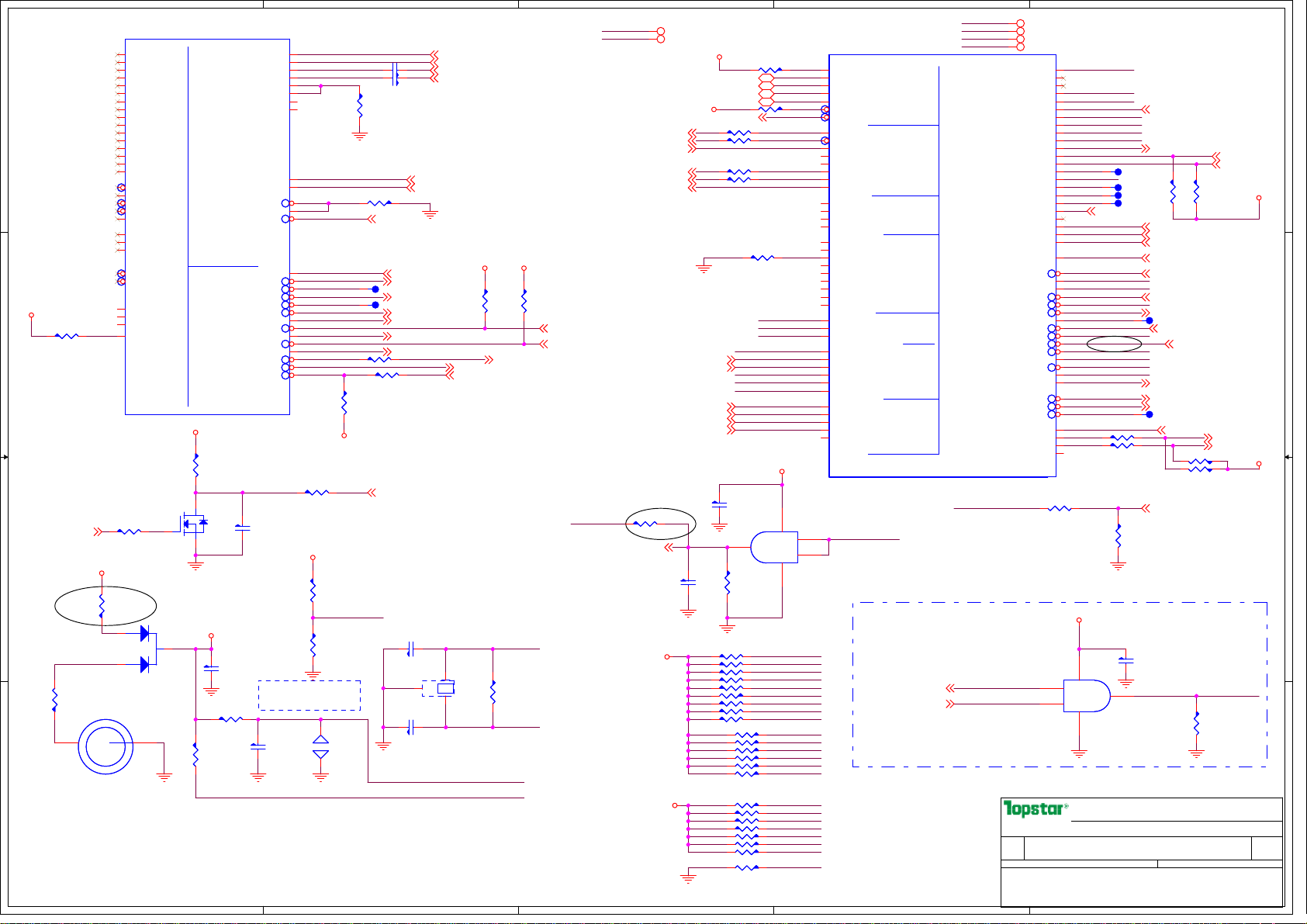
5
TGP
U1LB
U1LB
TGP
A20GATE
A20M#
CPUSLP#
IGNNE#
INIT3_3V#
INIT#
INTR
FERR#
NMI
RCIN#
SERIRQ
SMI#
STPCLK#
?
?
3
3
AE6
AD6
AC7
AD7
AE8
AD8
AD9
AC9
AD4
AC4
AD11
AC11
AD25
U16
Y20
Y21
Y18
AD21
AC25
AB24
Y22
T17
AC21
AA16
AA21
V18
AA20
CPUSLP#
SATA0RXN
SATA0RXP
SATA0TXN
SATA0TXP
SATA1RXN
SATA1RXP
SATA1TXN
SATA
SATA
HOST
HOST
SATA1TXP
SATA_CLKN
SATA_CLKP
SATARBIAS#
SATARBIAS
SATALED#
THERMTRIP#
U18C
U18C
R12
RSVD03
AE20
RSVD04
AD17
RSVD05
AC15
RSVD06
AD18
RSVD07
Y12
RSVD08
AA10
RSVD09
AA12
RSVD10
Y10
RSVD11
R0402
R0402
AD15
W10
V12
AE21
AE18
AD19
U12
AC17
AB13
AC13
AB15
Y14
AB16
AE24
AE23
AA14
V14
AD16
AB11
AB10
AD23
RSVD12
RSVD13
RSVD14
RSVD15
RSVD16
RSVD17
RSVD18
RSVD19
RSVD20
RSVD21
RSVD22
RSVD23
RSVD24
RSVD25
RSVD26
RSVD27
RSVD28
RSVD29
RSVD30
RSVD31
GPIO36
TGP
TGP
D D
+V3.3S
R446 10K
R446 10K
C C
+V3.3S
+V1.05S
R144
R144
10K
10K
R0402
R0402
VRM_PWRGD
3
Q4
R143
R143
1K
1K
R0402
R0402
CK505_CLK_EN#6,35
B B
EC_RTC
R11
R11
1K
1K
R0402
R0402
1
ns
ns
1
Q4
2N7002
2N7002
SOT23
SOT23
ns
ns
2
+V3.3A_RTC
3
C13
R455
R455
1M
1M
R0402
R0402
C13
1uF/10V,X7R
1uF/10V,X7R
C0603
C0603
R458
R458
20K
20K
R0402
R0402
D2
2
R9
R9
1K
1K
R0402
R0402
1
CR2032_DH
CR2032_DH
A A
VCC
RTCBAT1
RTCBAT1
GND
D2
BAT54C
BAT54C
SOT23
SOT23
2
5
R512 0 R0402
R512 0 R0402
C143
C143
0.1uF/10V,X5R
0.1uF/10V,X5R
C0402
C0402
ns
ns
+V3.3A_RTC
CMOS Settings J1
Clear CMOS Shunt
Keep CMOS Open
C338
C338
1uF/10V,X7R
1uF/10V,X7R
C0603
C0603
ns
ns
Reserved R512 ,NS Q4,R143 for POWER GOOD
R12
R12
332K,1%
332K,1%
R0402
R0402
ICH_INTVRMEN
R10
R10
0
0
R0402
R0402
ns
ns
12
CLR_CMOS1
CLR_CMOS1
JOPEN
JOPEN
RESISTOR_1
RESISTOR_1
ns
ns
4
C3270.01uF/25V,X7RC0402 C3270.01uF/25V,X7RC0402
C3260.01uF/25V,X7RC0402 C3260.01uF/25V,X7RC0402
R433
R433
0
0
R0402
R0402
R43524.9,1%R0402 R43524.9,1%R0402
HDD_LED# 23
H_A20GATE 25
H_A20M# 7
T24 nsT24 ns
H_IGNNE# 7
T25 nsT25 ns
H_INIT# 7
H_INTR 7
H_NMI 7
INT_SERIRQ 25
R444 0 R0402R444 0 R0402
R442 0 R0402R442 0 R0402
R441
R441
56
56
R0402
R0402
CK505_CLK_EN# 6,35
100315
C316
C316
4
SATA_RXN0 17
SATA_RXP0 17
SATA_TXN0 17
SATA_TXP0 17
CLK_ICH_SATA# 6
CLK_ICH_SATA 6
H_STPCLK# 7
PM_THRMTRIP# 7,24
C317
C317
18pF/50V,NPO
18pF/50V,NPO
C0402
C0402
12
Y4
Y4
3
32.768KHz
32.768KHz
Assy
Assy
xd3_2X6
xd3_2X6
18pF/50V,NPO
18pF/50V,NPO
C0402
C0402
RTC_RST#
SM_INTRUDER#
+V1.05S
H_SMI# 7
RTCX2
R404
R404
56
56
R0402
R0402
RTCX1
R400
10M
10M
R0402
R0402
+V3.3S
090604
R445
R445
10K
10K
R0402
R0402
H_FERR# 7
H_RCIN# 25
PLT_RST#
3
HDA_BITCLK22
HDA_RST#22
HDA_SDATA_IN022
HDA_SDOUT22
HDA_SYNC22
CLK_ICH146
R513 0 R0402R513 0 R0402
BUF_PLT_RST#9,19,25,26
+V3.3AL
+V3.3S
3
+V5S 11,12,16,17,21,22,23,25,31,33,34,35
EC_RTC 29
+V3.3S
R414 10K R0402
+V3.3S
LPC_FRAME#19,25
R394 33 R0402R394 33 R0402
R397 33 R0402R397 33 R0402
R412 33 R0402R412 33 R0402
R405 33 R0402R405 33 R0402
R414 10K R0402
LPC_AD019,25
LPC_AD119,25
LPC_AD219,25
LPC_AD319,25
R434 10K R0402
R434 10K R0402
AA5
ns
ns
AA6
ns
ns
AA1
AA3
AE2
SMB_CLK16
SMB_DATA16
SPI_SO_ICH14
SPI_SI_ICH14
SPI_CE#_ICH14
SPI_SCK_ICH14
R340 0 R0402R340 0 R0402
SMB_ALERT#
SMB_CLK
SMB_DATA
SMB_LINK_ALERT#
SMLINK0
SMLINK1
SPI_SO_ICH
SPI_SI_ICH
SPI_CE#_ICH
SPI_SCK_ICH
RTCX1
RTCX2
RTC_RST#
AA2
AD1
AC2
+V3.3AL
C172
C172
0.1uF/10V,X5R
0.1uF/10V,X5R
C0402
C0402
ns
ns
C358
C358
R162
R162
0.1uF/10V,X5R
0.1uF/10V,X5R
100K
100K
C0402
C0402
R0402
R0402
ns
ns
ns
ns
R126 10K R0402R126 10K R0402
R368 10K R0402R368 10K R0402
R365 10K R0402R365 10K R0402
R356 10K R0402R356 10K R0402
R343 10K R0402R343 10K R0402R400
1KR358 R04021KR358 R0402
R118 10K R0402R118 10K R0402
R371 10K R0402R371 10K R0402
R134 10K R0402R134 10K R0402
1KR342 R04021KR342 R0402
1KR341 R04021KR341 R0402
1KR388 R04021KR388 R0402
1KR362 R04021KR362 R0402
1KR132 R04021KR132 R0402
1KR124 R04021KR124 R0402
1KR439 R04021KR439 R0402
R437 10K R0402R437 10K R0402
R443 8.2K R0402R443 8.2K R0402
R436 4.7K R0402R436 4.7K R0402
1KR410 R0402ns 1KR410 R0402ns
1KR408 R0402ns 1KR408 R0402ns
1KR145 R04021KR145 R0402
1KR344 R04021KR344 R0402
VCC
VCC
4
GND
GND
SMB_LINK_ALERT#
SMLINK0
SMLINK1
SMB_ALERT#
PM_BATLOW#
PCIE_WAKE#
SYS_RST#
PM_RI#
EXT_SMI#
PM_CLKRUN#
HDA_SDOUT
53
1
2
GPIO12
GPIO13
GPIO14
GPIO15
GPIO8
GPIO9
ICH_SYNC#
PM_THRM#
INT_SERIRQ
HDA_SYNC
GPIO0
GPIO25
U7
U7
74AHC1G08GV
74AHC1G08GV
SOT23_5
SOT23_5
ns
ns
U18D
U18D
LDRQ1#/GPIO23
V6
LAD0/FWH0
LAD1/FWH1
Y5
LAD2/FWH2
W8
LAD3/FWH3
Y8
LDRQ0#
Y4
LFRAME#
P6
HDA_BIT_CLK
U2
HDA_RST#
W2
HDA_SDI0
V2
HDA_SDIN1
P8
HDA_SDIN2
HDA_SDOUT
Y1
HDA_SYNC
CLK14
U3
EE_CS
EE_DIN
T6
EE_DOUT
V3
EE_SHCLK
T4
LAN_CLK
P7
LANR_STSYNC
B23
LAN_RST#
LAN_RXD0
LAN_RXD1
LAN_RXD2
W3
LAN_TXD0
T7
LAN_TXD1
U4
LAN_TXD2
W4
RTCX1
V5
RTCX2
T5
RTCRST#
E20
SMBALERT#/GPIO11
H18
SMBCLK
E23
SMBDATA
H21
SMLALERT#
F25
SMLINK0
F24
SMLINK1
R2
TGP
TGP
SPI_MISO
T1
SPI_MOSI
M8
SPI_CS#
P9
SPI_CLK
R4
SPI_ARB
PLT_RST#
U1LB
U1LB
2
+V3.3S 6,7,9,10,11,12,13,14,16,17,19,21,22,23,24,25,26,31,32,33,34,35
+V1.05S 6,7,10,16,24,31,32,34
+V3.3A_RTC 16
+V3.3AL 12,14,16,18,19,21,23,25,26,27,28,29,30,31,32,33,35
GPIO0
GPIO6
GPIO7
GPIO8
GPIO9
GPIO10
GPIO12
GPIO13
GPIO14
GPIO15
STP_PCI#
STP_CPU#
GPIO24
GPIO25
GPIO26
GPIO27
GPIO28
CLKRUN#
GPIO33
GPIO34
GPIO38
GPIO39
THRM#
PWRBTN#
SUSCLK
PLTRSTB
WAKE#
PWROK
RSMRST#
INTVRMEN
SPKR
SLP_S3#
SLP_S4#
SLP_S5#
BATLOW#
DPRSTP#
DPSLP#
RSVD31
R432
T15
W16
W14
GPIO8
K18
GPIO9
H19
M17
GPIO12
A24
GPIO13
C23
GPIO14
P5
GPIO15
E24
AB20
Y16
AB19
T23 ICTPnsT23 ICTPns
R3
GPIO25
C24
T15 ICTPnsT15 ICTPns
D19
T18 ICTPnsT18 ICTPns
D20
T19 ICTPnsT19 ICTPns
F22
AC19
PM_CLKRUN# 25
U14
AC1
AC23
AC24
AB22
PM_THRM#
AB17
VRM_PWRGD
V16
ICH_SYNC#
AC18
E21
H23
RI#
G22
ICH_SUSCLK
D22
SYS_RST#
G18
PLT_RST#
G23
C25
SM_INTRUDER#
T8
PM_ICH_PWROK
U10
RSMRST#
AC3
ICH_INTVRMEN
AD3
J16
H20
E25
PM_SLP_S5#
F21
PM_BATLOW#
B25
R409 0 R0402R409 0 R0402
AB23
R438 0 R0402R438 0 R0402
AA18
F20
R0402R432
R0402
12
100
100
BM_BUSY#/GPIO0
DPRSLPVR
VRMPWRGD
MCH_SYNC#
SYS_RESET#
INTRUDER#
LPC AUDIO LAN
LPC AUDIO LAN
EPROM
EPROM
RTC SMB SPI
RTC SMB SPI
TGP
TGP
CPUPWRGD/GPIO49
MISC
MISC
SUS_STAT#/LPCPD#
?
?
RSMRST#
PM_RI#
T16 ICTPnsT16 ICTPns
T17 ICTPnsT17 ICTPns
R431
R431
10K
10K
R0402
R0402
1
EXT_SMI# 25
PM_DPRSLPVR 9
R500
R500
R496
R496
10K
10K
10K
10K
R0402
R0402
R0402
R0402
ns
ns
ns
ns
BOARDID_0 16
BOARDID_1 16
BOARDID_2 16
H_PWROK 7
PM_THRM# 7
PM_PWRBTN# 25
PM_SUS_STAT# 12,25
SYS_RST# 25
PCIE_WAKE# 19,25,26
PC_BEEP 22
PM_SLP_S3# 25,32
PM_SLP_S4# 25,34
PM_BATLOW# 25
R440 56nsR0402R440 56nsR0402
R407 56nsR0402R407 56nsR0402
PM_RSMRST# 25,32
PM_STP_PCI# 6
PM_STP_CPU# 6
+V3.3S
EC
H_DPRSTP# 7
H_DPSLP# 7
+V1.05S
+V3.3S
C171
C171
0.1uF/10V,X5R
0.1uF/10V,X5R
C0402
53
VCC
VCC
EC_MAIN_PWROK25
IMVP_PWRGD9,25,35
74AHC1G08GV
74AHC1G08GV
Page Name
Page Name
Page Name
Size
Size
Size
Date: Sheet of
Date: Sheet of
Date: Sheet
PROPERTY NOTE: this document contains information confidential and property to
PROPERTY NOTE: this document contains information confidential and property to
PROPERTY NOTE: this document contains information confidential and property to
TOPSTAR and shall not be reproduced or transferred to other documents or disclosed
TOPSTAR and shall not be reproduced or transferred to other documents or disclosed
TOPSTAR and shall not be reproduced or transferred to other documents or disclosed
to others or used for any purpose other than that for which it was obtained without
to others or used for any purpose other than that for which it was obtained without
to others or used for any purpose other than that for which it was obtained without
the expressed written consent of TOPSTAR
the expressed written consent of TOPSTAR
2
the expressed written consent of TOPSTAR
1
2
GND
GND
U6
U6
SOT23_5
SOT23_5
Project Name Rev
Project Name Rev
Project Name Rev
A3
A3
A3
C0402
4
TOPSTAR TECHNOLOGY
TOPSTAR TECHNOLOGY
TOPSTAR TECHNOLOGY
)
)
Swain Xu(
Swain Xu(
Swain Xu(
ICH7_M(2 of 4)
ICH7_M(2 of 4)
ICH7_M(2 of 4)
P01
P01
P01
)
1
PM_ICH_PWROK
R158
R158
10K
10K
R0402
R0402
of
15 39Friday, April 30, 2010
15 39Friday, April 30, 2010
15 39Friday, April 30, 2010
A
A
A
Page 16

5
+V3.3S
D10
D10
1N4148WS
1N4148WS
1
1
SOD323
SOD323
TGP
U1LB
U1LB
POWER
POWER
SMB_DATA
SMB_CLK
TGP
6mA
F12
VCC5REF
10mA
VCCRTC
V_CPU_IO
VCC1_5_1
VCC1_5_2
VCC1_5_3
VCC1_5_4
VCC3_3_1
VCC3_3_2
VCC3_3_3
VCC3_3_4
VCC3_3_5
VCC3_3_6
?
?
3
5
5
R339
R339
2.2K
2.2K
R0402
R0402
Q20
Q20
2N7002
2N7002
SOT23
SOT23
F5
45mA
Y6
6uA
AE3
24mA
Y25
10mA
F6
14mA
W18
1.5A
AA8
M9
M20
N22
1A
J10
K17
P15
V10
0.22A
H25
AD13
F10
G10
R10
T9
F18
N4
K7
0.1A
F1
NEAR PIN F1 NEAR PIN K7,N4 NEAR PIN F18
Q21
Q21
2N7002
2N7002
SOT23
SOT23
3
1
2
1
+V5S
VCC5REF_SUS
VCCSATAPLL
VCCDMIPLL
VCCUSBPLL
VCC1_05_1
VCC1_05_2
VCC1_05_3
VCC1_05_4
VCCSUS3_3_1
VCCSUS3_3_2
VCCSUS3_3_3
VCCSUS3_3_4
+V3.3AL
R338
R338
2.2K
2.2K
R0402
R0402
5
+V1.05S
C127
C127
C0402
C0402
C131
C131
C0402
C0402
+V3.3S
2
1uF/10V,X7R
1uF/10V,X7R
VCCDMIPLL
1uF/10V,X5R
1uF/10V,X5R
0.1UF/10V,X5R
0.1UF/10V,X5R
R295
R295
2.2K
2.2K
R0402
R0402
C138
C138
C0402
C0402
C132
C132
C0402
C0402
C141
C141
C0402
C0402
ns
ns
1uF/10V,X5R
1uF/10V,X5R
R294
R294
2.2K
2.2K
R0402
R0402
U18E
D D
C C
B B
A A
U18E
TGP
TGP
SMB_DATA15
SMB_CLK15
+V5S
R119
R119
100
100
R0402
R0402
C113
C113
C0603
C0603
C110
C110
C0402
C0402
ns
ns
ns
ns
1uF/10V,X5R
1uF/10V,X5R
1uF/10V,X5R
1uF/10V,X5R
C146
C146
C0402
C0402
1uF/10V,X5R
1uF/10V,X5R
C145
C145
C0402
C0402
ns
ns
1uF/10V,X5R
1uF/10V,X5R
C108
C108
C0402
C0402
1uF/10V,X5R
1uF/10V,X5R
SMB_DATA_S 6,13,19
SMB_CLK_S 6,13,19
4
1N4148WS
1N4148WS
SOD323
SOD323
C156
C156
C134
C134
C0805
C0805
C0402
C0402
10uF/6.3V,X5R
10uF/6.3V,X5R
C128
C128
C0805
C0805
1uF/10V,X5R
1uF/10V,X5R
C112
C112
C0402
C0402
+V3.3AL
C124
C124
C0402
C0402
1uF/10V,X5R
1uF/10V,X5R
4
+V3.3AL +V5AL
D11
D11
1
1
0.1uF/10V,X5R
0.1uF/10V,X5R
+V1.5S
C328
C328
C0402
C0402
0.1UF/10V,X5R
0.1UF/10V,X5R
C155
C155
C0402
C0402
ns
ns
0.1UF/10V,X5R
0.1UF/10V,X5R
0.1UF/10V,X5R
0.1UF/10V,X5R
+V1.05S
10uF/6.3V,X5R
10uF/6.3V,X5R
C162
C162
C0402
C0402
0.1UF/10V,X5R
C107
C107
C0805
C0805
10uF/6.3V,X5R
10uF/6.3V,X5R
0.1UF/10V,X5R
ns
ns
0.1UF/10V,X5R
0.1UF/10V,X5R
R121
R121
R0402
R0402
C109
C109
C0402
C0402
10
10
+V3.3A_RTC
C325
C325
C0402
C0402
0.1UF/10V,X5R
0.1UF/10V,X5R
ns
ns
VCCDMIPLL
C149
C149
C0402
C0402
0.01uF/25V,Y5V
0.01uF/25V,Y5V
+V3.3S
+V3.3S
C154
C154
C0402
C0402
ns
ns
0.1uF/10V,X5R
0.1uF/10V,X5R
C148
C148
4.7uF/10V,Y5V
4.7uF/10V,Y5V
C0805
C0805
R413
R413
10K
10K
R0402
R0402
ns
ns
R411
R411
10K
10K
R0402
R0402
C158
C158
C0805
C0805
10uF/6.3V,X5R
10uF/6.3V,X5R
R148 0 R0805R148 0 R0805
OPTION FOR FB
ns
ns
R415
R415
10K
10K
R0402
R0402
R426
R426
10K
10K
R0402
R0402
ns
ns
3
R150 0 R0805R150 0 R0805
OPTION FOR FB
R429
R429
10K
10K
R0402
R0402
ns
ns
R416
R416
10K
10K
R0402
R0402
3
+V1.5S
+V1.5S
Fuction P.M2 P.M1 P.M0
P02
X01
X03
X01i
0 0 0
0 0 1
0 1 0
0 1 1
BOARDID_0 15
BOARDID_1 15
BOARDID_2 15
2
+V3.3S 6,7,9,10,11,12,13,14,15,17,19,21,22,23,24,25,26,31,32,33,34,35
+V3.3AL 12,14,15,18,19,21,23,25,26,27,28,29,30,31,32,33,35
+V5S 11,12,17,21,22,23,25,31,33,34,35
+V3.3A_RTC 15
+V1.5S 10,14,19,23,33,34
+V1.05S 6,7,10,15,24,31,32,34
+V5AL 12,21,29,30,31,32,33
U1LB
U1LB
TGP
TGP
U18F
U18F
U1LB
U1LB
TGP
TGP
Page Name
Page Name
Page Name
Size
Size
Size
Project Name Rev
Project Name Rev
Project Name Rev
A3
A3
A3
Date: Sheet
Date: Sheet
Date: Sheet
PROPERTY NOTE: this document contains information confidential and property to
PROPERTY NOTE: this document contains information confidential and property to
PROPERTY NOTE: this document contains information confidential and property to
TOPSTAR and shall not be reproduced or transferred to other documents or disclosed
TOPSTAR and shall not be reproduced or transferred to other documents or disclosed
TOPSTAR and shall not be reproduced or transferred to other documents or disclosed
to others or used for any purpose other than that for which it was obtained without
to others or used for any purpose other than that for which it was obtained without
to others or used for any purpose other than that for which it was obtained without
the expressed written consent of TOPSTAR
the expressed written consent of TOPSTAR
2
the expressed written consent of TOPSTAR
ICH7_M(2 of 3)
ICH7_M(2 of 3)
ICH7_M(2 of 3)
1
A1
VSS
A25
VSS
B6
VSS
B10
VSS
B16
VSS
B20
VSS
B24
VSS
E18
VSS
F16
VSS
G4
VSS
G8
VSS
H1
VSS
H4
VSS
H5
VSS
K4
VSS
K8
VSS
K11
VSS
K19
VSS
K20
VSS
L4
VSS
M7
VSS
M11
VSS
N3
VSS
N12
VSS
N13
VSS
N14
VSS
N23
VSS
P11
VSS
P13
VSS
P19
VSS
R14
VSS
R22
VSS
T2
VSS
T22
VSS
V1
VSS
V7
VSS
V8
VSS
V19
VSS
V22
VSS
V25
VSS
W12
VSS
W22
VSS
Y2
VSS
Y24
VSS
AB4
VSS
AB6
VSS
AB7
VSS
AB8
VSS
AC8
VSS
AD2
VSS
AD10
VSS
AD20
VSS
AD24
VSS
AE1
VSS
AE10
VSS
AE25
VSS
G24
VSS
AE13
VSS
F2
VSS
AE16
RSVD32
TOPSTAR TECHNOLOGY
TOPSTAR TECHNOLOGY
TOPSTAR TECHNOLOGY
Swain Xu(
Swain Xu(
Swain Xu(
P01
P01
P01
1
?
?
)
)
)
A
A
A
of
of
of
16 39Thursday, April 29, 2010
16 39Thursday, April 29, 2010
16 39Thursday, April 29, 2010
Page 17
5
4
3
2
1
+V5S 11,12,16,21,22,23,25,31,33,34,35
+V3.3S 6,7,9,10,11,12,13,14,15,16,19,21,22,23,24,25,26,31,32,33,34,35
D D
SATA HDD
+V5S V_HDD
SATA_HDD
FB20 0 R0805FB20 0 R0805
C320
C320
4.7uF/10V,Y5V
4.7uF/10V,Y5V
C0805
C0805
C318
C318
0.1UF/10V,X5R
0.1UF/10V,X5R
C0402
C0402
C319
C319
0.1UF/10V,X5R
0.1UF/10V,X5R
C0402
C0402
Close to connector as possible
the same distance to connector
SATA_TXP015
SATA_TXN015
SATA_RXN015
SATA_RXP015
C297 0.01uF/25V,X7R C0402C297 0.01uF/25V,X7R C0402
C298 0.01uF/25V,X7R C0402C298 0.01uF/25V,X7R C0402
V3.3_SATA
+V3.3S V3.3_SATA
C C
B B
FB19 0 R0805 nsFB19 0 R0805 ns
C308
C308
4.7uF/10V,Y5V
4.7uF/10V,Y5V
C0805
C0805
ns
ns
C312
C312
0.1UF/16V,Y5V
0.1UF/16V,Y5V
C0402
C0402
ns
ns
C311
C311
0.1UF/16V,Y5V
0.1UF/16V,Y5V
C0402
C0402
ns
ns
V_HDD
SATA_B1
SATA_B1
Screw 2*5mm
Screw 2*5mm
Assembly
Assembly
711000000117
711000000117
SATA_HDD
SATA CONN
SATA CONN
SATA_D_50B_1
SATA_D_50B_1
2
TX
3
TX#
5
RX#
6
RX
8
VCC3_0
9
VCC3_1
10
VCC3_2
14
VCC5_0
15
VCC5_1
16
VCC5_2
18
REEVE
20
VCC12_0
21
VCC12_1
22
VCC12_2
SATA_B2
SATA_B2
Screw 2*5mm
Screw 2*5mm
Assembly
Assembly
711000000117
711000000117
GND0
GND1
GND2
GND3
GND4
GND5
GND6
GND7
GND8
GND9
1
4
7
11
12
13
17
19
23
24
TOPSTAR TECHNOLOGY
TOPSTAR TECHNOLOGY
TOPSTAR TECHNOLOGY
Swain Xu(
Swain Xu(
Swain Xu(
)
)
)
Page Name
Page Name
A A
5
4
3
Page Name
Size
Size
Size
Project Name Rev
Project Name Rev
Project Name Rev
A4
A4
A4
Date: Sheet
Date: Sheet
Date: Sheet
PROPERTY NOTE: this document contains information confidential and property to
PROPERTY NOTE: this document contains information confidential and property to
PROPERTY NOTE: this document contains information confidential and property to
TOPSTAR and shall not be reproduced or transferred to other documents or disclosed
TOPSTAR and shall not be reproduced or transferred to other documents or disclosed
TOPSTAR and shall not be reproduced or transferred to other documents or disclosed
to others or used for any purpose other than that for which it was obtained without
to others or used for any purpose other than that for which it was obtained without
to others or used for any purpose other than that for which it was obtained without
the expressed written consent of TOPSTAR
the expressed written consent of TOPSTAR
the expressed written consent of TOPSTAR
2
SATA HDD
SATA HDD
SATA HDD
P01
P01
P01
A
A
A
17 39Friday, April 30, 2010
17 39Friday, April 30, 2010
17 39Friday, April 30, 2010
of
of
of
1
Page 18
5
4
All of by-pass capacitors must be closed to IC
3
2
+V3.3AL 12,14,15,16,19,21,23,25,26,27,28,29,30,31,32,33,35
1
D3.3V
D D
0.1UF/10V,X5R
0.1UF/10V,X5R
U8
U8
37
Clk12M-out
SM_CE
SM_WP
DGND
EE_SDA
C C
USB_CR_PP614
USB_CR_PN614
D3.3V
GND_USB
EE_SCL
D3.3V
DGND
GPIO7
38
Clk12M_out
39
SM_CE/SD_WP
40
SM_WP/SD_CLK/MS_CLK
41
VSS
42
SM_WR
43
EE_SDA
44
EE_CLK
45
AVDD33
46
DP
47
DM
48
AVSS
IT1337E-48D/BX
IT1337E-48D/BX
QFPS48_0D5_1D6
QFPS48_0D5_1D6
C190
C190
C0402
C0402
GND_USB
D3.3V
REG18V
REG18V
36
35
34
33
GPIO6
REG33Vin
REG18Vout
SM/SD/MS D7
IT1337E-48
IT1337E-48
SD/MS/xD
SD/MS/xD
XTALO1XTALI2xD_CD3Clk48M4SM_WP_SW/SD_CMD/MS_BS5SM_RD/MS_INS6SM_RNB/SD_CD7SM/SD/MS D08SM/SD/MS D19SM_CLE10SM/SD/MS D211VDD18
CR_USB48
XTALI
XTALO
SM_WPSW
DGND
DGND
32
29
30
26
31
27
TC
VSS
GPIO5
GPIO128GPIO4
SM/SD/MS D6
SM/SD/MS D5
SM_RNB
SM_D1
SM_D2
VDD18
SM_D0
25
REG33Vout
12
VDD18
REG3.3V
REG5Vin
GPIO0/LED
SM/SD/MS D4
SM/SD/MS D3
SM_CD
SM_ALE
PWR_SW
RST
GPIO3
ClkSel
VDD33
VSS
24
23
22
RST
21
20
ClkSel
19
SM_D3
18
17
16
15
14
13
PWR_SW2
DGND
GND_USB
RST
GND_USB
D3.3V
C195
C195
0.1UF/10V,X5R
0.1UF/10V,X5R
C0402
C0402
R165
R165
30K
30K
R0402
R0402
C175
C175
4.7uF/10V,X5R
4.7uF/10V,X5R
C0805
C0805
GND_USB
use 48Mhz crystal
B B
REG3.3V
GND_USB
REG3.3V
R0603
R0603
C177
C177
0.1UF/10V,X5R
0.1UF/10V,X5R
C0402
C0402
ClkSel
R164 0
R164 0
CR_USB48 6
R167 0R0402R167 0R0402
C180
C180
4.7uF/10V,X5R
4.7uF/10V,X5R
C0805
C0805
0R504
0R504
R188 0 R0402R188 0 R0402
R0402
R0402
GND_USB
D3.3V
GND_USB GND_USB
+V3.3AL
SD_CLKSM_WP
R168 0nsR0402R168 0nsR0402
C187
C187
2.2UF/10V,X5R
2.2UF/10V,X5R
C0603
C0603
VDD18REG18V
C182
C182
0.1UF/10V,X5R
0.1UF/10V,X5R
C0402
C0402
SM_RNB
SM_WPSW
SM_D0
SM_D1
SM_D2
SM_D3
SD_CLK
SM_CE
OLD 2IN1 CONN.
J3
10
11
2
7
8
9
1
5
J3
CD
CMD
DAT0
DAT1
DAT2
CD/DAT3
CLK
SD_WP
2 in 1 Card
2 in 1 Card
VDD
VSS1
VSS2
G1
G2
G3
G4
SD_MMC
SD_MMC
4
3
6
12
13
14
15
GND_USB
C362
C362
0.1UF/10V,X5R
0.1UF/10V,X5R
GND_USB GND_USB
PWR_SW2
C361
C361
1uF/10V,X7R
1uF/10V,X7R
C0603
C0603
R174 0
R174 0
XTALO
R0402
R0402
R0402
R0402
ns
ns
Clk12M-out
EXT-12M
Int-12MHz
Ext-12MHz
R177 0
R177 0
C186
C186
GND_USBGND_USB
27pF/50V,NPO
27pF/50V,NPO
C0402
C0402
ns
ns
Y5
Y5
12.000MHz
12.000MHz
XS2_3D3
XS2_3D3
ns
ns
1 2
C189
C189
R0402ns
R0402ns
3
27pF/50V,NPO
27pF/50V,NPO
C0402
C0402
ns
ns
GND_USB
IT1337E-48 PIN MUX
PINs
SM/xD
SM_WPSW
05
06 MS_INS
SM_RD
SM_RNB
07
SM_D0
09
SM_D1
11
SM_D2
SM_D3
18
SM_D4
22
29
SM_D5
3208SM_D6
34
SM_D7
SM_CE
39
SM_WP
40
SD/MMC
SD_CMD
SD_CD
SD_D0
SD_D1
SD_D2
SD_D3
SD_D4
SD_D5
SD_D6
SD_D7
SD_WP
SD_CLK
2
MS_BS
MS_D0
MS_D1
MS_D2
MS_D3
MS_D4
MS_D5
MS_D6
MS_D7
MS_CLK
MS
TOPSTAR TECHNOLOGY
TOPSTAR TECHNOLOGY
TOPSTAR TECHNOLOGY
Swain Xu(
Swain Xu(
Swain Xu(
Page Name
Page Name
Page Name
Size
Size
Size
Project Name Rev
Project Name Rev
Project Name Rev
A3
A3
A3
Date: Sheet
Date: Sheet
Date: Sheet
PROPERTY NOTE: this document contains information confidential and property to
PROPERTY NOTE: this document contains information confidential and property to
PROPERTY NOTE: this document contains information confidential and property to
TOPSTAR and shall not be reproduced or transferred to other documents or disclosed
TOPSTAR and shall not be reproduced or transferred to other documents or disclosed
TOPSTAR and shall not be reproduced or transferred to other documents or disclosed
to others or used for any purpose other than that for which it was obtained without
to others or used for any purpose other than that for which it was obtained without
to others or used for any purpose other than that for which it was obtained without
the expressed written consent of TOPSTAR
the expressed written consent of TOPSTAR
the expressed written consent of TOPSTAR
Card Reader(UB6232 USB)
Card Reader(UB6232 USB)
Card Reader(UB6232 USB)
P01
P01
P01
1
)
)
)
A
A
18 39Thursday, April 29, 2010
18 39Thursday, April 29, 2010
18 39Thursday, April 29, 2010
A
of
of
of
R187 0
R187 0
D3.3V
EEprom Setting
U10
U10
1
A0
2
A1
3
A2
VSS4SDA
ns
ns
GND_USB
A A
5
S0=P12=EEP_SDA
S1=P13=EEP_SCK
8
VCC
7
WP
6
SCL
5
S-24CS02AFJ-TB-G
S-24CS02AFJ-TB-G
SO8_50_150
SO8_50_150
EE_SCL
EE_SDA
GND_USB
C193
C193
0.1UF/10V,X5R
0.1UF/10V,X5R
C0402
C0402
ns
ns
R189
R189
R190
R190
0
0
0
0
R0402
R0402
R0402
R0402
ns
ns
4
XTALI
use 12Mhz crystal
Page 19

5
+DATA4
D D
D40
D40
ESDPAD_R0603
ESDPAD_R0603
EGA1-0603-V05
EGA1-0603-V05
ns
ns
-DATA4
12
12
D39
D39
ESDPAD_R0603
ESDPAD_R0603
EGA1-0603-V05
EGA1-0603-V05
ns
ns
4
+V3.3S +V3.3AL
R155
R155
0
0
R0603
R0603
ns
ns
+V3.3S_PCIE +V3.3AL_PCIE
MPCIE2
MPCIE2
MINIPCIE_TEMP1
MINIPCIE_TEMP1
2
R459
R459
0
0
R0603
R0603
52
R451
R451
0
0
R0603
R0603
24
+V3.3S
R452
R452
0
0
R0603
R0603
ns
ns
48
+V1.5S
28
3
+V3.3S 6,7,9,10,11,12,13,14,15,16,17,21,22,23,24,25,26,31,32,33,34,35
+V3.3AL 12,14,15,16,18,21,23,25,26,27,28,29,30,31,32,33,35
+V1.5S 10,14,16,23,33,34
+VDC 12,21,27,29,30,31,32,33,34,35
2
1
change pcie nut part reference 091027
PCIE_NUT2
PCIE_NUT2
MINI_HOLE
MINI_HOLE
th_230_118_6
1122334455667
6
th_230_118_6
7
Keep USB2.0 Signal stub short
+3.3V1
R453 0 R0402R453 0 R0402
R454 0 R0402R454 0 R0402
CHK5
CHK5
90ohm@100M0.33A
90ohm@100M0.33A
l4_0805 ns
+VDC
l4_0805 ns
R477 0 nsR0402R477 0 nsR0402
R478 0 DebugR0402R478 0 DebugR0402
R489 0 R0402R489 0 R0402
R493 0 DebugR0402R493 0 DebugR0402
R484 0 R0402R484 0 R0402
R485 0 DebugR0402R485 0 DebugR0402
R480 0 DebugR0402R480 0 DebugR0402
R481 0 DebugR0402R481 0 DebugR0402
R482 0 DebugR0402R482 0 DebugR0402
R483 0 DebugR0402R483 0 DebugR0402
MINICARD_USB_PN414
MINICARD_USB_PP414
C C
WIFI OptionDebug Option
CLK_PCIE_EXPCARD#6
CLK_PCIE_EXPCARD6
PCIE_TXN1_SLOT14
PCIE_TXP1_SLOT14
PCIE_RXN1_SLOT14
PCIE_RXP1_SLOT14
BUF_PLT_RST#9,15,25,26
PCI_CLK_DEBUG6
LPC_FRAME#15,25 PWR_SW_VCC2 21,29
LPC_AD015,25
LPC_AD115,25
LPC_AD215,25
LPC_AD315,25
-DATA4
43
12
PICE_39
+DATA4
36
USB_D-
38
USB_D+
11
REFCLK-
13
REFCLK+
31
PETN0
33
PETP0
23
PERN0
25
PERP0
17
RESERVED0
19
RESERVED1
37
RESERVED_PCIE0
39
RESERVED_PCIE1
41
RESERVED_PCIE2
43
RESERVED_PCIE3
45
RESERVED_PCIE4
47
RESERVED_PCIE5
49
RESERVED_PCIE6
51
RESERVED_PCIE7
+3.3V0
+1.5V0
+1.5V1
+3.3VAUX
PCIE mini Card
PCIE mini Card
+1.5V2
LED_WPAN#
LED_WLAN#
LED_WWAN#
PERST#
WAKE#
CLKREQ#
SMB_DATA
SMB_CLK
CHANNEL_CLK
CHANNEL_DATA
RESERVED_DISABLE
RESERVED_SIM0
RESERVED_SIM1
RESERVED_SIM2
RESERVED_SIM3
RESERVED_SIM4
ns ICTP
ns ICTP
46
ns ICTP
ns ICTP
44
ns ICTP
ns ICTP
42
22
minicard_Wake#
1
minicard_CLKREQ#
7
32
30
5
3
20
16
14
12
10
8
T28
T28
T32
T32
T27
T27
ns
ns
ns
ns
R486 0 nsR0402R486 0 nsR0402
R490 0 nsR0402R490 0 nsR0402
R456 0 nsR0402R456 0 nsR0402
R457 0 nsR0402R457 0 nsR0402
R461 0 R0402R461 0 R0402
T29
T29
ICTP
ICTP
R464 0 nsR0402R464 0 nsR0402
R463 0 nsR0402R463 0 nsR0402
R462 0 nsR0402R462 0 nsR0402
T26
T26
ICTP
ICTP
+V3.3AL
BUF_PLT_RST# 9,15,25,26
PCIE_WAKE# 15,25,26
PCIE_CLKREQ# 6
SMB_DATA_S 6,13,16
SMB_CLK_S 6,13,16
R0402
R0402
10K
10K
R460
R460
HW_RATIO_OFF1# 25
EC_DEBG_UTXD 25
EC_DEBG_URXD 25
minicard_CLKREQ#
minicard_Wake#
+V3.3S
R488
R488
10K
10K
R0402
R0402
ns
ns
+V3.3AL
R487
R487
10K
10K
R0402
R0402
ns
ns
B B
GND0
GND1
GND2
GND5
GND4
+V3.3AL
+V3.3S
+V1.5S
C331
C331
10UF/6.3V,X5R
10UF/6.3V,X5R
C0805
C0805
ns
A A
ns
5
R492 0 R0603R492 0 R0603
R491 0 R0603ns R491 0 R0603ns
C333
C333
0.1UF/10V,X5R
0.1UF/10V,X5R
C0402
C0402
ns
ns
PICE_39
C336
C336
0.1UF/10V,X5R
0.1UF/10V,X5R
C0402
C0402
ns
ns
C332
C332
0.1UF/10V,X5R
0.1UF/10V,X5R
C0402
C0402
4
C334
C334
0.1UF/10V,X5R
0.1UF/10V,X5R
C0402
C0402
GND3
9
15
21
35
29
27
4
GND7
GND6
18
GND8
26
GND9
34
GND10
50
40
GND11
GND1253GND13
54
PCIE MINI CARD
PCIE MINI CARD
3
+V3.3S_PCIE
C170
C170
10UF/6.3V,X5R
10UF/6.3V,X5R
C0805
C0805
ns
ns
2
C335
C335
0.1UF/10V,X5R
0.1UF/10V,X5R
C0402
C0402
Page Name
Page Name
Page Name
Size
Size
Size
Project Name Rev
Project Name Rev
Project Name Rev
A3
A3
A3
Date: Sheet
Date: Sheet
Date: Sheet
PROPERTY NOTE: this document contains information confidential and property to
PROPERTY NOTE: this document contains information confidential and property to
PROPERTY NOTE: this document contains information confidential and property to
TOPSTAR and shall not be reproduced or transferred to other documents or disclosed
TOPSTAR and shall not be reproduced or transferred to other documents or disclosed
TOPSTAR and shall not be reproduced or transferred to other documents or disclosed
to others or used for any purpose other than that for which it was obtained without
to others or used for any purpose other than that for which it was obtained without
to others or used for any purpose other than that for which it was obtained without
the expressed written consent of TOPSTAR
the expressed written consent of TOPSTAR
the expressed written consent of TOPSTAR
+V3.3AL_PCIE
C330
C330
10UF/6.3V,X5R
10UF/6.3V,X5R
C0805
C0805
TOPSTAR TECHNOLOGY
TOPSTAR TECHNOLOGY
TOPSTAR TECHNOLOGY
Swain Xu(
Swain Xu(
Swain Xu(
PCIE MINI SLOT 1
PCIE MINI SLOT 1
PCIE MINI SLOT 1
P01
P01
P01
1
C337
C337
0.1UF/10V,X5R
0.1UF/10V,X5R
C0402
C0402
)
)
)
A
A
19 39Friday, April 30, 2010
19 39Friday, April 30, 2010
19 39Friday, April 30, 2010
A
of
of
of
Page 20

5
D D
C C
4
3
2
1
B B
A A
Page Name
Page Name
Page Name
Size
Size
Size
Project Name Rev
Project Name Rev
Project Name Rev
A3
A3
A3
Date: Sheet
Date: Sheet
Date: Sheet
PROPERTY NOTE: this document contains information confidential and property to
PROPERTY NOTE: this document contains information confidential and property to
PROPERTY NOTE: this document contains information confidential and property to
TOPSTAR and shall not be reproduced or transferred to other documents or disclosed
TOPSTAR and shall not be reproduced or transferred to other documents or disclosed
TOPSTAR and shall not be reproduced or transferred to other documents or disclosed
to others or used for any purpose other than that for which it was obtained without
to others or used for any purpose other than that for which it was obtained without
to others or used for any purpose other than that for which it was obtained without
the expressed written consent of TOPSTAR
the expressed written consent of TOPSTAR
5
4
3
2
the expressed written consent of TOPSTAR
TOPSTAR TECHNOLOGY
TOPSTAR TECHNOLOGY
TOPSTAR TECHNOLOGY
Swain Xu(
Swain Xu(
Swain Xu(
Blank
Blank
Blank
X03
X03
X03
1
)
)
)
A
A
A
of
of
of
20 39Thursday, April 29, 2010
20 39Thursday, April 29, 2010
20 39Thursday, April 29, 2010
Page 21
5
+V5AL_USB1
12
D36
D36
ESDPAD_R0603
ESDPAD_R0603
EGA1-0603-V05
EGA1-0603-V05
ns
ns
USB2
USB2
5
HOLE0
GND_USB
6
HOLE1
7
HOLE2
8
HOLE3
SINGLE USB PORT
SINGLE USB PORT
USB1G_1
USB1G_1
USB1
USB1
5
HOLE0
6
HOLE1
7
HOLE2
8
HOLE3
SINGLE USB PORT
SINGLE USB PORT
USB1G_1
USB1G_1
Update USB footprint to USB1F
D D
C C
GND_USB
B B
VCC1
-DATA1
+DATA1
GND
VCC1
-DATA1
+DATA1
GND
081215
8
GND
7
GND
6
GND
5
GND
U21
U21
P2793A
P2793A
SO8_50_150
SO8_50_150
GND_USB
4
3
2
1
D33
D33
ESDPAD_R0603
ESDPAD_R0603
EGA1-0603-V05
EGA1-0603-V05
+V5AL_USB1
4
3
2
1
EN/FON#
VOUT
VSET
Change C289 to F source
Swain 080814
C302
C302
330PF/50V,X7R
330PF/50V,X7R
C0402
C0402
GND_USB
-DATA0
+DATA0
12
GND_USB GND_USB
C290
C290
330PF/50V,X7R
330PF/50V,X7R
C0402
C0402
ns
ns
GND_USB
-DATA1
+DATA1
D30
D30
ESDPAD_R0603
ESDPAD_R0603
EGA1-0603-V05
EGA1-0603-V05
R69
R69
10K
10K
ns
ns
1
2
VIN
3
4
C283
C283
4.7UF/10V,Y5V
4.7UF/10V,Y5V
C0805
C0805
C101
C101
+
+
100uF/10V
100uF/10V
ct7343_28
ct7343_28
Keep USB2.0 Signal
stub short
12
D34
D34
ESDPAD_R0603
ESDPAD_R0603
EGA1-0603-V05
EGA1-0603-V05
C84
C84
+
+
100uF/10V
100uF/10V
ns
ns
ct7343_28
ct7343_28
GND_USB
12
+V5S+V3.3S
12
GND_USB
C468
C468
2.2uF/10V,X5R
2.2uF/10V,X5R
R293
R293
200K R0402
200K R0402
C284
C284
0.1UF/10V,X5R
0.1UF/10V,X5R
C0402
C0402
GND_USB
D31
D31
ESDPAD_R0603
ESDPAD_R0603
EGA1-0603-V05
EGA1-0603-V05
R366
R366
300K
300K
R0402
R0402
12
D32
D32
ESDPAD_R0603
ESDPAD_R0603
EGA1-0603-V05
EGA1-0603-V05
ns
ns
Keep USB2.0 Signal stub short
Vfan
+V3.3S
4
S2
S2
1.6A
1.6A
FUSE1812
FUSE1812
1 2
C57
C57
1000pF/50V,X7R
1000pF/50V,X7R
ns
ns
R86
R86
4.7K
4.7K
R0402
R0402
560KR361 R0402560KR361 R0402
C300
C300
1000pF/50V,X7R
1000pF/50V,X7R
C0402
C0402
USB_PORT_OC0#14
CHK4
nsCHK4
ns
1 2
4 3
l4_0805
l4_0805
90ohm@100M0.33A
90ohm@100M0.33A
R336 0 R0603R336 0 R0603
R335 0 R0603R335 0 R0603
CHK3 L4_0805 nsCHK3 L4_0805 ns
43
12
R291 0 R0603R291 0 R0603
R290 0 R0603R290 0 R0603
+V5S +V3.3S
R73
R73
10K
10K
ns
ns
R66 1K
R66 1K
ns
ns
D9
D9
C64
C64
1N4148WS
1N4148WS
2.2uF/10V,X5R
2.2uF/10V,X5R
SOD323
SOD323
1 2
FAN1_V 25
+V5AL
Install C429 for OC# issue
Swain 080815
GND_USB
USB_PORT_PN0 14
USB_PORT_PP0 14
USB_PORT_PN1 14
USB_PORT_PP1 14
+V3.3AL
R67
R67
10K
10K
ns
ns
FAN_TACH_ON
1
2 3
CPUFAN1
CPUFAN1
1
1
4
2
2
3
3
5
Econn
Econn
CNS3_R
CNS3_R
R68
R68
10K
10K
Q1
Q1
2N2222
2N2222
SOT23
SOT23
ns
ns
4
5
GND_USB
DEL 2 hole 090908
GND_USB
FAN_FB
FAN_BACK 25
R740R74
0
3
PWR_SW
PWR_SW
Button_4P
Button_4P
BUTTON4_S
BUTTON4_S
SWVCC1
2
112
334
4
SWVCC2_SW
PC1
PC1
1000pF/50V,X7R
1000pF/50V,X7R
C0402
C0402
U1
U1
APX9132A
APX9132A
SOT23_A
SOT23_A
VS+
Output
GND
2
PR1 10K R0402PR1 10K R0402
100KPR2 R0402100KPR2 R0402
PC2
PC2
1000pF/50V,X7R
1000pF/50V,X7R
C0402
C0402
+V3.3AL
1
2
GND_USB
3
1000pF/50V,X7R
1000pF/50V,X7R
PZ1
PZ1
BZT52C5V6S
BZT52C5V6S
SOD323
SOD323
1 2
C2
C2
0.1UF/10V,X5R
0.1UF/10V,X5R
C1
C1
C0402
C0402
1
+V3.3S 6,7,9,10,11,12,13,14,15,16,17,19,22,23,24,25,26,31,32,33,34,35
+V3.3AL 12,14,15,16,18,19,23,25,26,27,28,29,30,31,32,33,35
+V5S 11,12,16,17,22,23,25,31,33,34,35
+V5AL 12,16,29,30,31,32,33
+VDC 12,19,27,29,30,31,32,33,34,35
+V3.3AL
PR138
PR138
20K
20K
R0402
R0402
Isense_SYSP 27,36
12
ESD1
ESD1
EGA1-0603-V05
EGA1-0603-V05
ESDPAD_R0603
ESDPAD_R0603
ns
ns
GND_USB
3
PQ37
PQ37
2N7002E-T1
2N7002E-T1
SOT23
1
PR137
PR137
1M
1M
R0402
R0402
SOT23
2
PWR_SW_VCC2 19,29
LIDR# 12,25
PC95
PC95
1000pF/50V,X7R
1000pF/50V,X7R
C0402
C0402
+V3.3AL
3
PWRSW# 25
2
PD16
PD16
BAT54S
BAT54S
SOT23
SOT23
ns
ns
1
A A
FAN1_V=3.30V,Vfan=5V
FAN1_V=2.65V,Vfan=4V
FAN1_V=1.98V,Vfan=3V
5
4
3
2
Page Name
Page Name
Page Name
Size
Size
Size
Project Name Rev
Project Name Rev
Project Name Rev
A3
A3
A3
Date: Sheet
Date: Sheet
Date: Sheet
PROPERTY NOTE: this document contains information confidential and property to
PROPERTY NOTE: this document contains information confidential and property to
PROPERTY NOTE: this document contains information confidential and property to
TOPSTAR and shall not be reproduced or transferred to other documents or disclosed
TOPSTAR and shall not be reproduced or transferred to other documents or disclosed
TOPSTAR and shall not be reproduced or transferred to other documents or disclosed
to others or used for any purpose other than that for which it was obtained without
to others or used for any purpose other than that for which it was obtained without
to others or used for any purpose other than that for which it was obtained without
the expressed written consent of TOPSTAR
the expressed written consent of TOPSTAR
the expressed written consent of TOPSTAR
TOPSTAR TECHNOLOGY
TOPSTAR TECHNOLOGY
TOPSTAR TECHNOLOGY
Swain Xu(
Swain Xu(
Swain Xu(
)
)
Output Board
Output Board
Output Board
P01
P01
P01
)
1
A
A
21 39Friday, April 30, 2010
21 39Friday, April 30, 2010
21 39Friday, April 30, 2010
A
of
of
of
Page 22

5
+V3.3S
D D
T31 ICTP nsT31 ICTP ns
T30 ICTPnsT30 ICTP
HDA_RST#15
HDA_BITCLK15
HDA_SYNC15
HDA_SDOUT15
R471 51K R0402R471 51K R0402
BTL_BEEP25
R469 75K R0402R469 75K R0402
PC_BEEP15
C C
C348 1uF/10V,Y5V C0603C348 1uF/10V,Y5V C0603
C347 1uF/10V,Y5V C0603C347 1uF/10V,Y5V C0603
R470
R470
4.7K
4.7K
R0402
R0402
REMOVE SHUTDOWN#
R468
R468
4.7K
4.7K
R0402
R0402
HDA_SDATA_IN015
JACK_DET_A
C350
C350
100pF/50V,NPO
100pF/50V,NPO
C0402
C0402
MIC2_L
MIC2_R
INT_MIC_L
update internal MIC circuit
Layout Note:
All of JD resistors should be
placed as close as possible to
the sense pin of codec.
4
C351
C351
C0402
C0402
0.1UF/10V,X5R
0.1UF/10V,X5R
R472 33 R0402R472 33 R0402
C352 10pF/50V,NPO C0402
C352 10pF/50V,NPO C0402
C342 4.7uF/10V,X5R C0805C342 4.7uF/10V,X5R C0805
C341 4.7uF/10V,X5R C0805C341 4.7uF/10V,X5R C0805
C344 1uF/10V,X7R C0603C344 1uF/10V,X7R C0603
C343 1uF/10V,X7R C0603C343 1uF/10V,X7R C0603
0.1UF/10V,X5R
0.1UF/10V,X5R
A_GPIO0
A_GPIO1
ns
ns
ns
3
300ohm@100MHz,2A
300ohm@100MHz,2A
FB0805
FB0805
??
VCC5CDC
ns
ns
SURR_OUT_L
SURR_OUT_R
+V5SVCC5CDC
C199
C199
0.1UF/10V,X5R
0.1UF/10V,X5R
C0402
C0402
HP_OUT_L
HP_OUT_R
GND_AUD
INT_MIC_L_R
ns
ns
MIC2_REF
INT_MIC_L_R
JACK_DET_B
GND_AUD
FB16
FB16
C345
C355
GPIO0
GPIO1
REST#
BITCLK
SYNC
SDOUT
SDIN
PC-BEEP
JD1
LINE2-L
LINE2-R
MIC2-L
MIC2-R
CD-L
CD-R
MIC1-L
MIC1-R
LINE1-L
LINE1-R
C355
C0805
C0805
10UF/6.3V,X5R
10UF/6.3V,X5R
ALC662
9
VDD11VDD2
GND14GND27CD-GND19AGND126AGND2
C354
C354
C0402
C0402
2
3
11
6
10
5
8
12
13
14
15
16
17
18
20
21
22
23
24
0.1UF/10V,X5R
0.1UF/10V,X5R
38
AVDD125AVDD2
42
C357
C357
C0402
C0402
0.1UF/10V,X5R
0.1UF/10V,X5R
U19
U19
ALC662
ALC662
QFPS48_0D5_1D6
QFPS48_0D5_1D6
FRONT-OUT-L
FRONT-OUT-R
LINE1-VREFO-R
VREF
MIC1-VREFO-L
LINE1-VREFO-L
MIC2-VREFO
LINE2-VREFO
MIC1-VREFO-R
DCVOL
CEN-OUT
LFE-OUT
SIDESURR-OUT-L
SIDESURR-OUT-R
SPDIFI/EAPD
SPDIFO
SURR-OUT-L
JDREF
SURR-OUT-R
C345
C0402
C0402
JD2
35
36
37
27
28
29
30
31
32
33
34
43
44
45
46
47
48
39
40
41
1 2
C340
C340
C0805
C0805
10UF/6.3V,X5R
10UF/6.3V,X5R
Cross moat place
GND_AUD
C353 4.7uF/10V,X5R C0805C353 4.7uF/10V,X5R C0805
C356 4.7uF/10V,X5R C0805C356 4.7uF/10V,X5R C0805
C349 0.1UF/10V,X5R C0402C349 0.1UF/10V,X5R C0402
C346 10UF/6.3V,X5R C0805C346 10UF/6.3V,X5R C0805
VREFOUT
R473 4.7K R0402
R473 4.7K R0402
R474 2.2K R0402R474 2.2K R0402
R476 4.7K R0402R476 4.7K R0402
R475 10K R0402
R475 10K R0402
ns
ns
EAPD SHUTDOWN#
R495 0 R0402
R495 0 R0402
R494 20K,1% R0402R494 20K,1% R0402
ESDPAD_R0603
ESDPAD_R0603
EGA1-0603-V05
EGA1-0603-V05
MIC2_L
MIC2_R
MIC2_JD
D43
D43
ESDPAD_R0603
ESDPAD_R0603
EGA1-0603-V05
EGA1-0603-V05
2
HP_OUT_L
HP_OUT_R
D38
D38
MIC2_REF
R466 75 R0402R466 75 R0402
R465 75 R0402R465 75 R0402
12
0.1UF/10V,X5R
0.1UF/10V,X5R
R152 75 R0402R152 75 R0402
R149 75 R0402R149 75 R0402
HP_JD
12
0.1UF/10V,X5R
0.1UF/10V,X5R
C315
C315
C0402
C0402
100pF/50V,NPO
100pF/50V,NPO
D41
D41
1N4148WS
1N4148WS
1 2
SOD323
SOD323
D42
D42
1N4148WS
1N4148WS
1 2
SOD323
SOD323
R0402
R0402
C339
C339
100pF/50V,NPO
100pF/50V,NPO
C0402
C0402
+V3.3S 6,7,9,10,11,12,13,14,15,16,17,19,21,23,24,25,26,31,32,33,34,35
+V5S 11,12,16,17,21,23,25,31,33,34,35
Headphone Jack
INPUT:HEADPHONE/LINE-OUT
OUTPUT:FRONT L/R
FB12 300ohm@100MHz,2A
FB12 300ohm@100MHz,2A
1 2
FB0805
FB0805
FB11 300ohm@100MHz,2A
FB11 300ohm@100MHz,2A
1 2
FB0805
FB0805
12
12
D14
D14
D13
D13
ESDPAD_R0603
ESDPAD_R0603
EGA1-0603-V05
EGA1-0603-V05
12
12
D19
D19
D18
D18
ESDPAD_R0603
ESDPAD_R0603
EGA1-0603-V05
EGA1-0603-V05
R156
R156
4.7K
4.7K
C161
C161
C168
C168
100pF/50V,NPO
100pF/50V,NPO
C0402
C0402
C0402
C0402
GND_AUD
R153
R153
4.7K
4.7K
R0402
R0402
FB14 300ohm@100MHz,2A
FB14 300ohm@100MHz,2A
FB13 300ohm@100MHz,2A
FB13 300ohm@100MHz,2A
C173
C173
C169
C169
100pF/50V,NPO
100pF/50V,NPO
C0402
C0402
C0402
C0402
ESDPAD_R0603
ESDPAD_R0603
EGA1-0603-V05
EGA1-0603-V05
Stereo Microphone Jack
INPUT:STEREO MIC-IN
OUTPUT:CENT/LFE
1 2
FB0805
FB0805
1 2
FB0805
FB0805
ESDPAD_R0603
ESDPAD_R0603
EGA1-0603-V05
EGA1-0603-V05
GND_AUD
1
1
4
2
5
6
3
7
8
LINE_OUT1
LINE_OUT1
L
L
R
R
AZALIAJACK
AZALIAJACK
AUDIO8B
AUDIO8B
MIC_IN1
MIC_IN1
1
4
2
5
6
3
7
8
AZALIAJACK
AZALIAJACK
AUDIO8B
AUDIO8B
L
L
R
R
GND_AUD
VCC5CDC VCC5CDC
Av(inv)
GAIN1
R185
R185
R180
R180
10K
10K
10K
10K
R0402
R0402
R0402
R0402
ns
GAIN0
GAIN1
B B
ns
Adjust Gain to 10dB
BY K' 080118
R181
R181
R183
R183
10K
10K
10K
10K
R0402
R0402
R0402
R0402
ns
ns
GND_AUD GND_AUD
GAIN0
00
10
10
1
1
6dB
10dB
15.6dB
21.6dB
Onboard Amp
U9
C194
C194
0.22uF/10V,X7R
0.22uF/10V,X7R
C0603
SURR_OUT_R
A A
SURR_OUT_L
C0603
C179 0.22uF/10V,X7R
C179 0.22uF/10V,X7R
GND_AUD
C178 0.22uF/10V,X7R
C178 0.22uF/10V,X7R
GND_AUD
C192
C192
0.22uF/10V,X7R
0.22uF/10V,X7R
C0603
C0603
Change R336,R326,R324 to 0 ohm
Swain 081120
5
R184 20K R0402R184 20K R0402
R166 10K R0402R166 10K R0402 FB10
C0603
C0603
C0603
C0603
R175 20K R0402R175 20K R0402
SHUTDOWN#
GAIN0
GAIN1
U9
APA2031
APA2031
sop20_0d65_4d4g
sop20_0d65_4d4g
17
RIN-
7
RIN+
9
LIN+
10
BYPASS
5
LIN-
12
NC
SHDWN#19GND1
2
GAIN0
3
GAIN1
ROUT+
ROUTLOUT+
LOUT-
PVDD1
PVDD2
GND2
GND3
GND4
GND5
C188
C188
C0402
C0402
0.1UF/10V,X7R
0.1UF/10V,X7R
4
INTSPR+
INTSPRINTSPL+
INTSPL-
VCC5CDC
0.1UF/10V,X7R
0.1UF/10V,X7R
18
14
4
8
16
VDD
6
15
1
11
13
20
21
HP_OUT_L JACK_DET_AHP_OUT_R
3456
2
1
De-pop Solution
R194 1K R0402R194 1K R0402
INTSPL-
INTSPL+
INTSPR+
INTSPR-
C183
C183
C0402
C0402
AMP_SHDW25
C181
C181
C0805
C0805
4.7uF/10V,Y5V
4.7uF/10V,Y5V
GND_AUD
GND_AUD GND_AUD
Q9
Q9
2N7002DW
2N7002DW
SC70_6
SC70_6
INTSPK1
INTSPK1
INT_spkR 4Pin
INT_spkR 4Pin
CNS4_R
CNS4_R
4
4
3
3
2
2
1
1
AMP_SHDWAMP_SHDW
VCC5CDC
R176
R176
10K
10K
R0402
R0402
3
1
2
R195
R195
10K
10K
R0402
R0402
6
6
5
5
2
Q10
Q10
2N7002
2N7002
R179
R179
100K
100K
R0402
R0402
GND_AUD
3
1
INT_MIC_L_R
INT_MIC_L
3456
R146
R146
R0402
R0402
Q6
Q6
2N7002DW
2N7002DW
SC70_6
SC70_6
SHUTDOWN#
1K
1K
100pF/50V,NPO
100pF/50V,NPO
onboard stereo
microphone
FB10
300ohm@100MHz,2A
300ohm@100MHz,2A
1 2
FB0805
FB0805
C135
C135
C0402
C0402
GND_AUD
12
D12
D12
ESDPAD_R0603
ESDPAD_R0603
EGA1-0603-V05
EGA1-0603-V05
ns
ns
MIC1
MIC1
Microphone
Microphone
BZ_D6027
BZ_D6027
+
+
ASSY
ASSY
1
2
2
JACK_DET_B
R479 20K,1% R0402R479 20K,1% R0402
R467 5.11K,1% R0402R467 5.11K,1% R0402
Layout Note:
Tied at three points under the
codec and near the codec
MIC2_JD
HP_JD
Page Name
Page Name
Page Name
Size
Size
Size
Project Name Rev
Project Name Rev
Project Name Rev
C
C
C
Date: Sheet
Date: Sheet
Date: Sheet
PROPERTY NOTE: this document contains information confidential and property to
PROPERTY NOTE: this document contains information confidential and property to
PROPERTY NOTE: this document contains information confidential and property to
TOPSTAR and shall not be reproduced or transferred to other documents or disclosed
TOPSTAR and shall not be reproduced or transferred to other documents or disclosed
TOPSTAR and shall not be reproduced or transferred to other documents or disclosed
to others or used for any purpose other than that for which it was obtained without
to others or used for any purpose other than that for which it was obtained without
to others or used for any purpose other than that for which it was obtained without
the expressed written consent of TOPSTAR
the expressed written consent of TOPSTAR
the expressed written consent of TOPSTAR
D20
D20
JOPEN_3
JOPEN_3
1 2
ns
ns
R157 0 R0402
R157 0 R0402
ns
ns
R182 0 R0402R182 0 R0402
C166
C191
FB15 300ohm@100MHz,2A
FB15 300ohm@100MHz,2A
C136
TOPSTAR TECHNOLOGY
TOPSTAR TECHNOLOGY
TOPSTAR TECHNOLOGY
Swain Xu(
Swain Xu(
Swain Xu(
Audio
Audio
Audio
P01
P01
P01
1
0.1UF/10V,X5R
0.1UF/10V,X5R
0.1UF/10V,X5R
0.1UF/10V,X5R
1 2
0.1UF/10V,X5R
0.1UF/10V,X5R
FB0805 ns
FB0805 ns
GND_AUD
)
)
)
nsC0402C166
nsC0402
nsC0402C191
nsC0402
nsC0402C136
nsC0402
22 39Friday, April 30, 2010
22 39Friday, April 30, 2010
22 39Friday, April 30, 2010
A
A
A
of
of
of
Page 23

5
D D
C C
TP_HDD_LED#
TP_CHG_LED#
TP_BTL_LED#
TP_POWERLED#
IDE+
CHARGE_LED
BAT_STATE_LED
PWR+
B B
C198
C198
0.1UF/10V,X5R
0.1UF/10V,X5R
C0402
C0402
+V3.3S
ns
ns
+V3.3AL
TESD6 EGA1-0603-V05
TESD6 EGA1-0603-V05
TESD4 EGA1-0603-V05
TESD4 EGA1-0603-V05
TESD3 EGA1-0603-V05
TESD3 EGA1-0603-V05
TESD5 EGA1-0603-V05
TESD5 EGA1-0603-V05
C201 1000pF/50V,X7R C0402ns C201 1000pF/50V,X7RC0402ns
C203 1000pF/50V,X7R C0402C203 1000pF/50V,X7R C0402
C204 1000pF/50V,X7R C0402C204 1000pF/50V,X7R C0402
C200 1000pF/50V,X7R C0402C200 1000pF/50V,X7R C0402
LED
IDE+
220R196 R0402
220R196 R0402
CHARGE_LED TP_CHG_LED#
220R203 R0402220R203 R0402
BAT_STATE_LED
220R202 R0402220R202 R0402
220R204 R0402220R204 R0402
1 2
ESDPAD_R0603ns
ESDPAD_R0603ns
1 2
ESDPAD_R0603ns
ESDPAD_R0603ns
1 2
ESDPAD_R0603ns
ESDPAD_R0603ns
1 2
ESDPAD_R0603ns
ESDPAD_R0603ns
1 2
HDD
HDD
BL-HB335A-TRB
BL-HB335A-TRB
TCHARGE
TCHARGE
LED4_1210B
LED4_1210B
HA1B333B AMP&BLUE
HA1B333B AMP&BLUE
Blue Color
3 1
Orange color
1 2
POWER
POWER
BL-HB335A-TRB
BL-HB335A-TRB
B
B
24
R
R
TP_CHG_LED#
TP_BTL_LED#
TP_POWERLED#
TP_HDD_LED#
ns
ns
TP_BTL_LED#
TP_POWERLED#PWR+
4
R200 10K R0402
R200 10K R0402
ns
ns
R199 10K R0402
R199 10K R0402
ns
ns
R201 10K R0402
R201 10K R0402
ns
ns
+V3.3S
CHG_LED# 25
BTL_LED# 25
POWERLED# 25
+V3.3AL
R447
R447
10K
10K
R0402
R0402
ns
ns
HDD_LED# 15
ns
ns
ns
ns
3
7
8
H11
H11
HOLE
HOLE
1
TH_S276_256_100
TH_S276_256_100
H8
H8
1
TH_256_100
TH_256_100
H4,H4 footprintTH_315_100
080820
HOLE
HOLE
ns
ns
TH_256_100A
TH_256_100A
ns
ns
TH_256_100A
TH_256_100A
H4
H4
1
1
1
2
2
3
3
7
4
4
5
5
8
6
6
CNS6_0D5_RA1
CNS6_0D5_RA1
INT_spkR 6Pin
INT_spkR 6Pin
TP
TP
H6
H6
HOLE
HOLE
1
ns
ns
H10
H10
HOLE
HOLE
1
TH_256_100
TH_256_100
ns
ns
GND_AUD
H3
H3
1
TH_256_100
TH_256_100
GND_BAT
HOLE
HOLE
+V5S
TPCLK 25
TPDAT 25
HOLE
HOLE
ns
ns
H1
H1
1
ns
ns
TH_276X236_100
TH_276X236_100
H9
H9
HOLE
HOLE
1
TH_256_100
TH_256_100
ns
ns
TH_256_100A
TH_256_100A
HOLE
HOLE
ns
ns
2
H2
H2
HOLE
HOLE
1
H5
H5
HOLE
HOLE
1
TH_S276_256_100
TH_S276_256_100
+V5S 11,12,16,17,21,22,25,31,33,34,35
+V3.3S 6,7,9,10,11,12,13,14,15,16,17,19,21,22,24,25,26,31,32,33,34,35
+V3.3AL 12,14,15,16,18,19,21,25,26,27,28,29,30,31,32,33,35
+V1.05S 6,7,10,15,16,24,31,32,34
+V1.5S 10,14,16,19,33,34
1
FD6
FD6
FD3
FD3
FD7
FD7
FD4
FD4
FD2
1
FMARKS
FMARKS
ns
ns
1
FD2
1
FMARKS
FMARKS
ns
ns
1
TOPSTAR TECHNOLOGY
TOPSTAR TECHNOLOGY
TOPSTAR TECHNOLOGY
Swain Xu(
Swain Xu(
Swain Xu(
)
)
Page Name
Page Name
Page Name
Size
Size
Size
Project Name Rev
Project Name Rev
Project Name Rev
A3
A3
A3
Date: Sheet
Date: Sheet
Date: Sheet
PROPERTY NOTE: this document contains information confidential and property to
PROPERTY NOTE: this document contains information confidential and property to
PROPERTY NOTE: this document contains information confidential and property to
TOPSTAR and shall not be reproduced or transferred to other documents or disclosed
TOPSTAR and shall not be reproduced or transferred to other documents or disclosed
TOPSTAR and shall not be reproduced or transferred to other documents or disclosed
to others or used for any purpose other than that for which it was obtained without
to others or used for any purpose other than that for which it was obtained without
to others or used for any purpose other than that for which it was obtained without
the expressed written consent of TOPSTAR
the expressed written consent of TOPSTAR
4
3
2
the expressed written consent of TOPSTAR
LED/WIFI/BT
LED/WIFI/BT
LED/WIFI/BT
P01
P01
P01
)
A
A
23 39Thursday, April 29, 2010
23 39Thursday, April 29, 2010
23 39Thursday, April 29, 2010
1
A
of
of
of
FD8
FD8
FD1
FMARKS
FMARKS
ns
ns
5
1
FD1
1
FMARKS
FMARKS
ns
ns
+V3.3AL
1
1
1
FMARKS
FMARKS
ns
ns
C222
C222
0.1UF/10V,X5R
0.1UF/10V,X5R
C0402
C0402
1
1
FMARKS
FMARKS
ns
ns
1
1
FMARKS
FMARKS
ns
ns
1
FD5
FD5
1
1
FMARKS
FMARKS
ns
ns
A A
Page 24

5
D D
4
3
2
+V1.05S 6,7,10,15,16,31,32,34
+V3.3S 6,7,9,10,11,12,13,14,15,16,17,19,21,22,23,25,26,31,32,33,34,35
1
+V3.3S
R186
R186
10K
10K
R0402
R0402
R173
R173
10K
10K
R0402
R0402
OVT_SHUTDOWN#7
C185
C185
1000pF/50V,X7R
R172
R172
100K
C C
100K
R0402
R0402
1000pF/50V,X7R
C0402
C0402
3456
1
2
Q8
Q8
MMDT3904
MMDT3904
SC70_6
SC70_6
3
Q5
Q5
2N7002E-T1
2N7002E-T1
SOT23
ALT_ON25
B B
1
R178
R178
100K
100K
R0402
R0402
SOT23
2
SHDN_LOCK#
PM_THRMTRIP#7,15
CPU
R171
R171
470
470
R0402
R0402
ns
ns
R170
R170
4.7K
4.7K
R0402
R0402
ns
ns
C184
R169
R169
100K
100K
R0402
R0402
ns
ns
C184
0.1uF/10V,X5R
0.1uF/10V,X5R
C0402
C0402
ns
ns
OVP CIRCUIT
VIN
+V1.05S
3456
R192
R192
4.7K
4.7K
R0402
R0402
ns
ns
R193
R193
100
100
R0402
R0402
ns
ns
1
R191
R191
1K
1K
R0402
R0402
ns
ns
2
Q7
Q7
MMDT3904
MMDT3904
SC70_6
SC70_6
ns
ns
SHDN_LOCK# 32
C196
C196
2.2uF/10V,X7R
2.2uF/10V,X7R
C0805
C0805
ns
ns
THRMTRIP#
THERM_ALERT#
Thermal
sensor
A A
5
4
3
AND
SHDN#
VDC
TOPSTAR TECHNOLOGY
TOPSTAR TECHNOLOGY
TOPSTAR TECHNOLOGY
Swain Xu(
Swain Xu(
Swain Xu(
)
)
Page Name
Page Name
Page Name
Size
Size
Size
Project Name Rev
Project Name Rev
Project Name Rev
A4
A4
A4
Date: Sheet
Date: Sheet
Date: Sheet
PROPERTY NOTE: this document contains information confidential and property to
PROPERTY NOTE: this document contains information confidential and property to
PROPERTY NOTE: this document contains information confidential and property to
TOPSTAR and shall not be reproduced or transferred to other documents or disclosed
TOPSTAR and shall not be reproduced or transferred to other documents or disclosed
TOPSTAR and shall not be reproduced or transferred to other documents or disclosed
to others or used for any purpose other than that for which it was obtained without
to others or used for any purpose other than that for which it was obtained without
to others or used for any purpose other than that for which it was obtained without
the expressed written consent of TOPSTAR
the expressed written consent of TOPSTAR
the expressed written consent of TOPSTAR
2
MDC&BT/FAN/OTP
MDC&BT/FAN/OTP
MDC&BT/FAN/OTP
P01
P01
P01
)
24 39Thursday, April 29, 2010
24 39Thursday, April 29, 2010
24 39Thursday, April 29, 2010
1
A
A
A
of
of
of
Page 25

5
+V3.3S
R367
R367
8.2K
8.2K
R0402
R0402
D37
D37
A20GATE
1N4148WS
1N4148WS
1
H_A20GATE15
D D
1
SOD323
SOD323
EC Output Signal!
del 2n7002 090909
+V3.3S
R359
R359
10K
10K
D35
D35
R0402
R0402
ns
ns
1
SCANOUT15
SCANOUT14
SCANOUT13
SCANOUT12
SCANOUT11
SCANOUT10
SCANOUT9
SCANOUT8
SCANOUT7
SCANOUT6
SCANOUT5
SCANOUT4
SCANIN0
SCANOUT3
SCANIN1
SCANIN2
SCANOUT2
SCANOUT1
SCANIN3
SCANIN4
SCANIN5
SCANOUT0
SCANIN6
SCANIN7
1
H_RCIN#15
1
1
2
2
3
3
4
4
5
27
5
27
6
28
6
28
7
7
8
8
9
9
C C
10
10
11
11
12
12
13
13
14
14
15
15
16
16
17
17
18
18
19
19
20
20
21
21
22
22
23
23
24
24
25
25
26
26
CNS26_1_R_UP
CNS26_1_R_UP
Econn
Econn
KBCON1
KBCON1
1N4148WS
1N4148WS
SOD323
SOD323
RCIN#
EC Output Signal!
+V3.3AL
R396 4.7K R0402
R396 4.7K R0402
EC_BUF_PLT_RST#
Connect PLTRST to EC_PCI_RST#
Swain 080819
BUF_PLT_RST#9,15,19,26
EC_V3.3AL
C142
C142
4.7UF/10V,Y5V
4.7UF/10V,Y5V
C0805
C0805
R141
R141
R137
R137
10K
10K
R0402
R0402
ns
ns
R399 0 R0402R399 0 R0402
R424 0 R0402R424 0 R0402
100,1%
100,1%
1
R0402
R0402
EC_PCI_RST#
EC_BUF_PLT_RST#
Q3
Q3
MMBT3904-F
MMBT3904-F
SOT23
SOT23
2 3
Fuction P.M2 P.M1 P.M0
VerA
0 0 0
VerB
+V3.3AL
B B
R450
R450
10K
10K
R0402
R0402
ns
ns
R423
R423
10K
10K
R0402
R0402
BIU configuration
should match flash
speed used
A A
EC_PROCHOT#7
R449
R449
10K
10K
R0402
R0402
ns
ns
R422
R422
10K
10K
R0402
R0402
R448
R448
10K
10K
R0402
R0402
ns
ns
PCB_Mark0
PCB_Mark1
PCB_Mark2
R421
R421
10K
10K
R0402
R0402
BIOS Ver: X.XX
BIOS Ver: X.XX
EC Ver: X.XX
EC Ver: X.XX
XXXXXXXX
XXXXXXXX
EC/BIOS Label
EC/BIOS Label
740601900104
740601900104
+V5S
2
R406 0 R0402R406 0 R0402
Verc
LABEL1
LABEL1
Topstar Soft
Topstar Soft
Q24
Q24
2N7002E-T1
2N7002E-T1
1
SOT23
SOT23
ns
ns
3
5
0 0 1
0 1 0
EC output Signal!
PROCHOT#
PCIE_WAKE#15,19,26
R128
R128
10K
10K
R0402
R0402
C125
C125
0.01uF/25V,X7R
0.01uF/25V,X7R
C0402
C0402
EC_RUNTIME_SCI#14
INT_SERIRQ15
LPC_FRAME#15,19
PM_CLKRUN#15
PM_RSMRST#15,32
SYS_RST#15
DDR3_DRAM_PWROK8,30,32
MAIN_PWROK32
EC_DEBG_UTXD19
EC_DEBG_URXD19
PM_BATLOW#15
4
EC_RESET#
A20GATE
RCIN#
EC_RESET#
PCI_CLK_EC6
LPC_AD015,19
LPC_AD115,19
LPC_AD215,19
LPC_AD315,19
BATT_IN#28
PWRSW#21
PM_SLP_S3#15,32
PM_SLP_S4#15,34
IMVP_ON35
V1_05S_ON31
V0_75S_ON30
ALWAYS_ON29
MAIN_ON33
IMVP_PWRGD9,15,35
V1_5S_ON33
ALW_PWROK29
V1.8S_ON31
V0_89S_ON31
4
EC_PCI_RST#
SCANIN7
SCANIN6
SCANIN5
SCANIN4
SCANIN3
SCANIN2
SCANIN1
SCANIN0
SCANOUT15
SCANOUT14
SCANOUT13
SCANOUT12
SCANOUT11
SCANOUT10
SCANOUT9
SCANOUT8
SCANOUT7
SCANOUT6
SCANOUT5
SCANOUT4
SCANOUT3
SCANOUT2
SCANOUT1
SCANOUT0
R402 1K R0402R402 1K R0402
LIDR#12,21
R391 0nsR0402R391 0nsR0402
AC_IN27
ALT_ON24
V1_5_ON30
PCIE_WAKE#_EC
R387 1K R0402R387 1K R0402
R3600R0402 R3600R0402
R374 1K R0402R374 1K R0402
The 0ohm RES will across the isolate
island of anolog GND and digital GND
R120 0 R0603R120 0 R0603
C114
C114
0.1UF/10V,X5R
0.1UF/10V,X5R
C0402
C0402
R4030R0402 R4030R0402
3
+V3.3S 6,7,9,10,11,12,13,14,15,16,17,19,21,22,23,24,26,31,32,33,34,35
+V3.3AL 12,14,15,16,18,19,21,23,26,27,28,29,30,31,32,33,35
+V5S 11,12,16,17,21,22,23,31,33,34,35
FB9
FB9
120ohm@100MHz,500mA
120ohm@100MHz,500mA
FB0603
FB0603
EC_V3.3AL
33
111
VCC
VCC
VCC96VCC
PS2
PS2
KB3926
KB3926
GPXIOA
GPXIOA
GPIO
GPIO
8051
8051
GND
GND35GND24GND
GND
11
94
113
3
22
9
VCC
VCC
FAN
FAN
PSCLK1/GPIO4A/P80CLK
PSDAT1/GPIO4B/P80DAT
SPI
SPI
CLK
CLK
C122
C122
0.1UF/10V,X5R
0.1UF/10V,X5R
C0402
C0402
1
GA20/GPIO00
2
KBRST#/GPIO01
20
SCI#/GPIO0E
37
ECRST#
12
PCICLK
3
SERIRQ
4
LFRAME#
10
LAD0
8
LAD1
7
LAD2
5
LAD3
13
PCIRST#/GPIO05
38
CLKRUN#/GPIO1D
62
KSI7/GPIO37
61
KSI6/GPIO36
60
KSI5/GPIO35
59
KSI4/GPIO34
58
KSI3/GPIO33
57
KSI2/GPIO32
56
KSI1/GPIO31
55
KSI0/GPIO30/E51_TXD(ISP)
82
KSO17/GPIO49
81
KSO16/GPIO48
54
KSO15/GPIO2F/E51_RXD(ISP)
53
KSO14/GPIO2E
52
KSO13/GPIO2D
51
KSO12/GPIO2C
50
KSO11/GPIO2B
49
KSO10/GPIO2A
48
KSO9/GPIO29
47
KSO8/GPIO28
46
KSO7/GPIO27
45
KSO6/GPIO26
44
KSO5/GPIO25
43
KSO4/GPIO24
42
KSO3/GPIO23/TP_ISP
41
KSO2/GPIO22/TP_ANA_TEST
40
KSO1/GPIO21/TP_PLL
39
KSO0/GPIO20/TP_TEST
6
GPIO04
14
GPIO07/i_clk_8051
15
GPIO08/i_clk_peri
16
GPIO0A
17
GPIO0B/ESB_CLK
18
GPIO0C/ESB_DAT_O/ESB_DAT_I
19
GPIO0D
32
GPIO18
36
GPIO1A/NUMLED#
73
GPIO40
74
GPIO41
89
GPIO50
127
GPIO59/TEST_CLKSPICLKI
68
GPO3C
70
GPO3D
71
GPO3E
72
GPO3F
76
GPI43
75
GPI42
90
E51CS#/GPIO52
30
E51TXD/GPIO16
31
E51RXD/GPIO17/E51CLK
92
E51TMR0/GPIO54/WDT_LED#
93
E51INT0/GPIO55/SCROLED#
91
E51TMR1/GPIO53/CAPSLED#
95
E51INT1/GPIO56
V18R
124
V18R
MSIC
MSIC
LPC
LPC
69
67
AGND
AVCC
KB
KB
1 2
R136
R136
0
0
R0805
R0805
125
U17
U17
ADC PWM
ADC PWM
AD0/GPI38
AD1/GPI39
AD2/GPI3A
AD3/GPI3B
PWM0/GPIO0F
PWM1/GPIO10
PWM2/GPIO11
PWM3/GPIO19
FANFB0/GPIO14
FANFB1/GPIO15
FANPWM0/GPIO12
FANPWM1/GPIO13
PSCLK2/GPIO4C
PSDAT2/GPIO4D
PSCLK3/GPIO4E
PSDAT3/GPIO4F
SMBUS
SMBUS
SDA1/GPIO47
SCL1//GPIO46
SDA0/GPIO45
SCL0/GPIO44
GPXIOA00/SDICS#
GPXIOA01/SDICLK
GPXIOA02/SDIMOSI
GPXIOA03
GPXIOA04
GPXIOA05
GPXIOA06
GPXIOA07
GPXIOA08
GPXIOA09
GPXIOA10
GPXIOA11
GPXIOD0/SDIMISO
GPXIOD
GPXIOD
GPXIOD1
GPXIOD2
GPXIOD3
GPXIOD4
GPXIOD5
GPXIOD6
GPXIOD7
MISO
MOSI
SPICLK/GPIO58
SPICS#
XCLK32K/GPIO57
XCLKI
XCLKO
KB3310B
KB3310B
+V3.3AL
C152
C152
0.1UF/10V,X5R
0.1UF/10V,X5R
C0402
C0402
63
HDD_ZOUT
64
HDD_YOUT
65
HDD_XOUT
66
21
23
25
34
28
29
26
27
83
84
85
86
EC_ICH_PWROK
87
EC_SMI#
88
80
79
78
77
GPXIOA00
97
98
99
100
101
102
103
104
PROCHOT#
105
106
107
108
109
EC_PM_SUS_STAT#
110
PCB_Mark0
112
PCB_Mark1
114
PCB_Mark2
115
116
117
EC_BUF_PLT_RST#
118
119
120
126
128
121
122
123
EC_V3.3AL
C150
C150
10UF/6.3V,X5R
10UF/6.3V,X5R
C0805
C0805
V18R
R4250R0402 R4250R0402
R2960R0402 R2960R0402
R4270R0402 R4270R0402
R4280R0402 R4280R0402
32XCLKI
32XCLKO
2
C160
C102
C102
0.1UF/10V,X5R
0.1UF/10V,X5R
C0402
C0402
ns
ns
Should have a 0.1uF capacitor close to every
GND-VCC pair + one larger cap on the supply.
C151
C151
1uF/10V,X7R
1uF/10V,X7R
C0603
C0603
SYS_I_Sense 36
BTL_BEEP 22
POWERLED# 23
SET_I 36
EC_BKLT_PWM 12
FAN_BACK 21
BT_DISABLE 23
FAN1_V 21
IVT_I_ADJ 12
TPCLK 23
TPDAT 23
HW_RATIO_OFF1# 19
R3980ns R0402 R3980ns R0402
I2C_DATA 7
I2C_CLK 7
SM_BAT_SDA2 28
SM_BAT_SCL2 28
CHG_LED# 23
R4180R0402 R4180R0402
AMP_SHDW 22
EC_IMVP_PD_OUT 35
CHG_ON 36
HW_OFF_BKLT# 12
CAM_PWRON 12
BTL_LED# 23
R4200R0402 R4200R0402
LVDS_BKLTEN 7,12
EC_IMVP_PD_IN# 35
EC_SPI_MISO
EC_SPI_MOSI
EC_SPI_SCK
EC_SPI_CS#
BT_PWRON 23
C160
0.1UF/10V,X5R
0.1UF/10V,X5R
C0402
C0402
ns
ns
EXT_SMI# 15
PM_PWRBTN# 15
R4191K
R4191K
R0402
R0402
2
C159
C159
0.1UF/10V,X5R
0.1UF/10V,X5R
C0402
C0402
C111
C111
100pF/50V,NPO
100pF/50V,NPO
C0402
C0402
EC_ICH_PWROK
MAIN_PWROK
+V3.3AL
R308
R308
4.7K
4.7K
R0402
R0402
EC_SPI_HOLD#
EC_SPI_SCK
EC_SPI_MOSI
+V3.3AL
PM_SUS_STAT# 12,15
+V3.3AL
PM_SLP_S4#
PM_SLP_S3#
C137
C137
100pF/50V,NPO
100pF/50V,NPO
C0402
C0402
ICH_PWROK from EC
Swain 080819
EC_SPI_WP#
EC_SPI_HOLD#
C167
C167
Page Name
Page Name
Page Name
PROPERTY NOTE: this document contains information confidential and property to
PROPERTY NOTE: this document contains information confidential and property to
PROPERTY NOTE: this document contains information confidential and property to
TOPSTAR and shall not be reproduced or transferred to other documents or disclosed
TOPSTAR and shall not be reproduced or transferred to other documents or disclosed
TOPSTAR and shall not be reproduced or transferred to other documents or disclosed
to others or used for any purpose other than that for which it was obtained without
to others or used for any purpose other than that for which it was obtained without
to others or used for any purpose other than that for which it was obtained without
the expressed written consent of TOPSTAR
the expressed written consent of TOPSTAR
the expressed written consent of TOPSTAR
1
C157
C126
C126
0.1UF/10V,X5R
0.1UF/10V,X5R
C0402
C0402
C157
0.1UF/10V,X5R
0.1UF/10V,X5R
C0402
C0402
GPXIOA00
HDD_ZOUT
HDD_YOUT
HDD_XOUT
CHG_ON
SYS_I_Sense
ns SPI pull up
EC_SPI_CS#
EC_SPI_MOSI
EC_SPI_MISO
EC_SPI_SCK
I2C_CLK
I2C_DATA
SM_BAT_SDA2
SM_BAT_SCL2
LIDR#
EC_IMVP_PD_IN#
PCIE_WAKE#_EC
ALT_ON
PWRSW#
EC_IMVP_PD_OUT
TPCLK
TPDAT
R390 0 R0402 nsR390 0 R0402 ns
R154 0 R0402R154 0 R0402
EC_SPI_CS#
8
VCC
7
HOLD#
6
CLK
5
D
U13
U13
W25Q80BV
W25Q80BV
SOIC8_50_208
SOIC8_50_208
C164
C164
18pF/50V,NPO
18pF/50V,NPO
C0402
C0402
12
3
Assy
Assy
18pF/50V,NPO
18pF/50V,NPO
C0402
C0402
Size
Size
Size
Project Name Rev
Project Name Rev
Project Name Rev
Custom
Custom
Custom
Date: Sheet
Date: Sheet
Date: Sheet
1
CS#
EC_SPI_MISO
2
Q
EC_SPI_WP#
3
W#
4
VSS
U20
U20
W25X40
W25X40
8
VDD
WP#
HOLD#
32XCLKI
R151
R151
10M
10M
R0402
R0402
32XCLKO
SO
CE#
SCK
VSS
090604
3
7
colay small package EC 091028
Y1
Y1
32.768KHz
32.768KHz
xd3_2X6
xd3_2X6
C144
C144
0.1UF/10V,X5R
0.1UF/10V,X5R
C0402
C0402
R417 10K
R417 10K
R0402
R0402
R357 10K
R357 10K
R0402
R0402
R363 10K
R363 10K
R0402
R0402
R369 10K
R369 10K
R0402
R0402
R122 10K R0402R122 10K R0402
C299 3300pF/50V,X7R
C299 3300pF/50V,X7R
C0402
C0402
R334 10K R0402 nsR334 10K R0402 ns
R306 10K R0402 nsR306 10K R0402 ns
R430 10K R0402 nsR430 10K R0402 ns
R305 10K R0402 nsR305 10K R0402 ns
R133 4.7K R0402R133 4.7K R0402
R138 4.7K R0402R138 4.7K R0402
R129 5.6K R0402R129 5.6K R0402
R125 5.6K R0402R125 5.6K R0402
R401 10K R0402R401 10K R0402
R127 10K R0402 nsR127 10K R0402 ns
R393 10K R0402R393 10K R0402
R147 10K nsR0402R147 10K nsR0402
R163 10K R0402
R163 10K R0402
R123 10K R0402 nsR123 10K R0402 ns
R140 10K R0402R140 10K R0402
ns
ns
R142 10K R0402R142 10K R0402
EC_MAIN_PWROK 15
R309 4.7K R0402 nsR309 4.7K R0402 ns
R307 4.7K R0402R307 4.7K R0402
nsSO8_50_150
nsSO8_50_150
EC_SPI_MOSI
5
SI
EC_SPI_MISO
2
EC_SPI_CS#
1
EC_SPI_SCK
6
4
TOPSTAR TECHNOLOGY
TOPSTAR TECHNOLOGY
TOPSTAR TECHNOLOGY
Swain Xu(
Swain Xu(
Swain Xu(
KBC(KB3310B)
KBC(KB3310B)
KBC(KB3310B)
P01
P01
P01
1
+V3.3AL
ADD R140 R142
leixy 090824
)
)
)
25 39Friday, April 30, 2010
25 39Friday, April 30, 2010
25 39Friday, April 30, 2010
+V3.3AL
of
of
of
C296
C296
1uF/10V,X7R
1uF/10V,X7R
C0603
C0603
A
A
A
Page 26
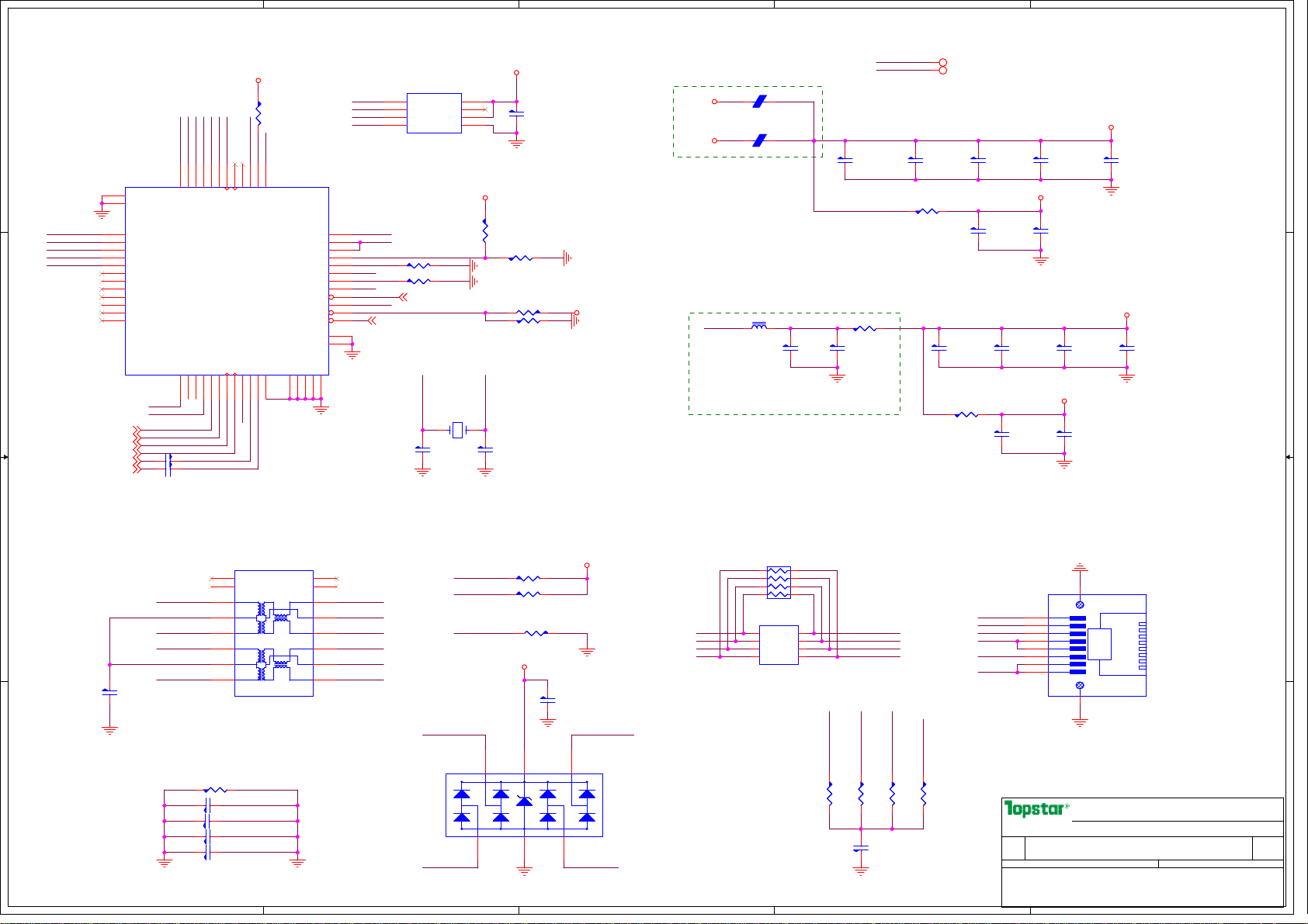
5
4
3
2
1
+V3.3AL 12,14,15,16,18,19,21,23,25,27,28,29,30,31,32,33,35
+V3.3S 6,7,9,10,11,12,13,14,15,16,17,19,21,22,23,24,25,31,32,33,34,35
VDD3D3_LAN
C34
C34
0.1uF/10V,X5R
0.1uF/10V,X5R
C0402
C0402
C55
C55
0.1uF/10V,X5R
0.1uF/10V,X5R
C0402
C0402
C61
C61
0.1uF/10V,X5R
0.1uF/10V,X5R
C0402
C0402
ns
ns
VDDREG
R90 0 R0603R90 0 R0603
C245
C245
4.7uF/10V,X5R
4.7uF/10V,X5R
C0805
C0805
C259
C259
0.1uF/10V,X5R
0.1uF/10V,X5R
C0402
C0402
Place close to VDD10 PINS.
C262
C262
0.1uF/10V,X5R
0.1uF/10V,X5R
C0402
C0402
R91 0 R0603R91 0 R0603
C266
C266
0.1uF/10V,X5R
0.1uF/10V,X5R
C0402
C0402
C40
C40
1uF/10V,X5R
1uF/10V,X5R
C0402
C0402
EVDD10
C261
C261
0.1uF/10V,X5R
0.1uF/10V,X5R
C0402
C0402
ns
ns
C62
C62
0.1uF/10V,X5R
0.1uF/10V,X5R
C0402
C0402
C279
C279
0.1uF/10V,X5R
0.1uF/10V,X5R
C0402
C0402
VDD10
C265
C265
0.1uF/10V,X5R
0.1uF/10V,X5R
C0402
C0402
8
7
6
5
VDD3D3_LAN
R78
R78
0
0
R0402
R0402
XTAL2
C46
C46
27pF/50V,NPO
27pF/50V,NPO
C0402
C0402
C63
C63
0.1uF/10V,X5R
0.1uF/10V,X5R
C0402
C0402
0R79 R0402 ns0R79 R0402 ns
1KR76 R04021KR76 R0402
15KR77 R040215KR77 R0402
+V3.3S
+V3.3AL
+V3.3S
FB18
1 2
300ohm@100MHz,2A
300ohm@100MHz,2A
FB17
FB17
ns
ns
1 2
300ohm@100MHz,2A
300ohm@100MHz,2A
L2
L2
REGOUT
1
1
4.7uH/1.22A
4.7uH/1.22A
LS2_3513
LS2_3513
FB0805FB18
FB0805
FB0805
FB0805
C466
C466
C0805
C0805
4.7uF/10V,X5R
4.7uF/10V,X5R
C36
C36
0.1uF/10V,X5R
0.1uF/10V,X5R
C0402
C0402
R92 0 R0603R92 0 R0603
C467
C467
C0402
C0402
0.1uF/10V,X5R
0.1uF/10V,X5R
Place close to VDD33_LAN PINS.
VDD3D3_LAN
ns
ns
U5
R89
R89
1K
1K
R0402
VDD3D3_LAN
42
41
AVDD33_1
DVDD10_3(NC)
EVDD10
40
VDD3D3_LAN
39
LED0
38
DVDD3_2
GPO/SMBALERT
23
R0402
EESK
37
LED1/EESK
GND
24
REGOUT
VDDREG_2
VDDREG_1
ENSWREG
EEDI/SDA
LED3/EEDO
EECS/SCL
DVDD10_2
LANWAKEB
DVDD33_1
ISOLATEB
PERSTB
G3G3G4G4G5G5G6G6G7
D D
XTAL2
XTAL1
RSET
VDD10
VDD3D3_LAN
VDD3D3_LAN
U4
U4
G1
G1
G2
G2
LAN_TX0+
VDD10
LAN_TX1+
LAN_TX1-
C C
PCIE_TXP0_LAN14
PCIE_TXN0_LAN14
CLK_PCIE_LAN6
CLK_PCIE_LAN#6
PCIE_RXP0_LAN14
PCIE_RXN0_LAN14
1
MDIP0
2
MDIN0
3
AVDD10_1
4
MDIP1
5
MDIN1
6
AVDD10_2(NC)
7
MDIP2(NC)
8
MDIN2(NC)
9
AVDD10_3(NC)
10
MDIP3(NC)
11
MDIN3(NC)
12
AVDD33_4(NC)
QFNS48_0D4_1G
QFNS48_0D4_1G
47
45
43
46
RSET
CKXTAL244CKXTAL1
AVDD33_348AVDD33_2
AVDD10_5
DVDD10_1
HSIP17HSIN18REFCLK_P19REFCLK_N20EVDD1021HSOP22HSON
SMBCLK(NC)14SMBDATA(NC)15CLKREQB
13
16
VDD10
CLKREQ#
C59 0.1UF/10V,X7RC0402C59 0.1UF/10V,X7RC0402
C60 0.1UF/10V,X7RC0402C60 0.1UF/10V,X7RC0402
EECS
EESK
EEDI/AUX
EEDO
REGOUT
36
VDDREGLAN_TX0-
35
34
33
EEDI/AUX
32
EEDO
31
EECS
30
VDD10
29
28
VDD3D3_LAN
27
26
25
G9
G9
G8
G8
G7
U5
1
CS
SK
DI
DO
93C46
93C46
so8_50_150
so8_50_150
VCC
NC1
NC2
GND
2
3
4
R692 10K R0402R692 10K R0402
R693 10K R0402R693 10K R0402
PCIE_WAKE# 15,19,25
BUF_PLT_RST# 9,15,19,25
XTAL1
Y2
Y2
25MHz
25MHz
XS2_3D3
XS2_3D3
1 2
C50
C50
27pF/50V,NPO
27pF/50V,NPO
C0402
C0402
VDD3D3_LAN
Place close to EVDD10 PINS
RN1
RN1
0x4
U11
U11
TRAN16_50_272
B B
LAN_TX0+
LAN_TX0- TX0LAN_TX1+
C223
C223
0.01uF/25V,X7R
0.01uF/25V,X7R
C0402
C0402
LAN_TX1-
TRAN16_50_272
13
N4
12
N3
9
TD-
11
TDC
10
TD+
15
RD-
14
RDC
16
RD+
1CT:1CT
1CT:1CT
1CT:1CT
1CT:1CT
CMT
RXC
TX+
RX+
PCIE_WAKE#
5
N2
4
N1
TX0+
8
TX-
MCT1
6
10K ohm close to Host side
7
TX1+
2
RX-
MCT2
3
TX1-
1
CLKREQ#
RSET
R689 10K R0402R689 10K R0402
R691 10K R0402R691 10K R0402
VDD3D3_LAN
VDD3D3_LAN
R592.49K,1%R0402 R592.49K,1%R0402
C39
C39
0.1uF/10V,X5R
0.1uF/10V,X5R
C0402
C0402
TX0+
TX0TX1+
LAN_TX1-LAN_TX1+
LD1
LD1
AZC099-04S
AZC099-04S
4
ns
ns
A A
R6 0 R0603nsR6 0 R0603ns
C8 330pF/50V,X7R C0402C8 330pF/50V,X7R C0402
5
6
0x4
RA0603_8
RA0603_8
1 2
3 4
5 6
7 8
CHK2
CHK2
ns
ns
L2+4L3+
3
L2-
2
L1+
1
L1-
100MHz0.5A
100MHz0.5A
CMC8
CMC8
RJ45_TX0+
5
6
L3-
7
L4+
8
L4-
RJ45_TX0+
RJ45_TX0RJ45_TX1+
RJ45_TX1-TX1-
MCT1
MCT2
MCT3
MCT4
R7
R7
R217
75
75
R0402
R0402
R217
75
75
R0402
R0402
R216
R216
75
75
R0402
R0402
R8
R8
75
75
R0402
R0402
RJ45_TX0RJ45_TX1+
MCT3
RJ45_TX1MCT4
C11 4.7uF/10V,Y5V C0805C11 4.7uF/10V,Y5V C0805
C6 330pF/50V,X7R C0402C6 330pF/50V,X7R C0402
C7 330pF/50V,X7R C0402C7 330pF/50V,X7R C0402
5
CASE_GND
1
3
2
LAN_TX0-LAN_TX0+
4
3
CASE_GND
C10
C10
1000pF/2000V
1000pF/2000V
C1206
C1206
2
CASE_GND
J4
J4
RJ45
RJ45
910
RJ45_SB
RJ45
RJ45
TX0+
TX0+
1
TX0-
TX0-
2
TX1+
TX1+
3
TX2+
TX2+
4
TX2-
TX2-
5
TX1-
TX1-
6
TX3+
TX3+
7
TX3-
TX3-
8
RJ45_SB
TX0+
TX0+
TX0-
TX0TX1+
TX1+
TX2+
TX2+
TX2-
TX2TX1-
TX1TX3+
TX3+
TX3-
TX3-
CASE_GND
TOPSTAR TECHNOLOGY
TOPSTAR TECHNOLOGY
TOPSTAR TECHNOLOGY
<OrgAddr1>
<OrgAddr1>
Page Name
Page Name
Page Name
Size
Size
Size
Project Name Rev
Project Name Rev
Project Name Rev
A3
A3
A3
Date: Sheet
Date: Sheet
Date: Sheet
PROPERTY NOTE: this document contains information confidential and property to
PROPERTY NOTE: this document contains information confidential and property to
PROPERTY NOTE: this document contains information confidential and property to
TOPSTAR and shall not be reproduced or transferred to other documents or disclosed
TOPSTAR and shall not be reproduced or transferred to other documents or disclosed
TOPSTAR and shall not be reproduced or transferred to other documents or disclosed
to others or used for any purpose other than that for which it was obtained with the
to others or used for any purpose other than that for which it was obtained with the
to others or used for any purpose other than that for which it was obtained with the
expressed written consent of TOPSTAR
expressed written consent of TOPSTAR
expressed written consent of TOPSTAR
<OrgAddr1>
RTL8101E/8111C(GLAN)
RTL8101E/8111C(GLAN)
RTL8101E/8111C(GLAN)
P01
P01
P01
1
26 39Friday, April 30, 2010
26 39Friday, April 30, 2010
26 39Friday, April 30, 2010
of
of
of
A
A
A
Page 27
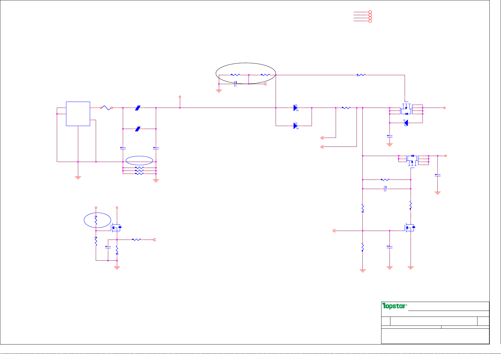
update PJ1 as N02
100315
PJ1
PJ1
DC JACK 5P
DC JACK 5P
PWR5P_DC3
PWR5P_DC3
5
SHLD2
4
SHLD1
AD+
AD-1
AD-2
2
Jack_GND
1
3
PF2
PF2
7A
7A
FUSE1206
FUSE1206
1 2
PFB3
PFB3
12
100ohm@100MHz,3A
100ohm@100MHz,3A
FB0805
FB0805
PFB4
PFB4
12
100ohm@100MHz,3A
100ohm@100MHz,3A
FB0805
FB0805
PC113
PC113
1uF/25V,Y5V
1uF/25V,Y5V
C0805
C0805
PR3 0 R0402nsPR3 0 R0402ns
PR5 0 R0402
PR5 0 R0402
ns
ns
PR4 0 R0402
PR4 0 R0402
ns
ns
AD+
3A
PC114
PC114
1uF/25V,Y5V
1uF/25V,Y5V
C0805
C0805
connect Jack_GND to GND 090915 240mil
PR177
PR177
30K
30K
S_Bot
S_Bot
PC115
PC115
0.1uF/25V,X7R
0.1uF/25V,X7R
C0603
C0603
R0402
R0402
ALW_EN
PR176
PR176
200K
200K
R0402
R0402
S_Bot
S_Bot
ALW_EN 29
PD20
PD20
1
1
SBM54PT
SBM54PT
SMB
SMB
PD19
PD19
1
1
SBM54PT
SBM54PT
SMB
SMB
BATT+ 28,33,36
+V3.3AL 12,14,15,16,18,19,21,23,25,26,28,29,30,31,32,33,35
+VDC 12,19,21,29,30,31,32,33,34,35
AD+ 33
PR17
PR17
10
10
R0402
R0402
PQ4
PQ4
AO4419
AO4419
SO8_50_150
SO8_50_150
3
2
1
PC13
PC13
0.1uF/25V,Y5V
0.1uF/25V,Y5V
C0402
C0402
PQ7
PQ7
AO4419
AO4419
SO8_50_150
SO8_50_150
R0402
R0402
4
G
G
D
D
5
S
S
1
1
PD2
PD2
SSM34PT
SSM34PT
SMA
SMA
1
2
3
S
S
G
G
4
5A5A
6
7
8
8
7
6
5
D
D
BATT+
+VDC
PC37
PC37
0.01uF/25V,X7R
0.01uF/25V,X7R
C0402
C0402
PR16
PR16
0.025,1%
0.025,1%
R2512
R2512
3A3A
ns
ns
Isense_SYSP21,36
Isense_SYSN28,32,36
5A 5A
PR54 510K
PR54 510K
0815VB:Change PR9 to 51K
Update PR175 TO 30k
bobo100315
PR175
PR175
510K
510K
R0402
R0402
PR174
PR174
510K
510K
R0402
R0402
PC116
C0402
C0402
+V3.3ALAD+
1
1000pF/50V,X7R
1000pF/50V,X7R
3
2
PR178
PR178
47K
47K
R0402
R0402
PQ44
PQ44
2N7002
2N7002
SOT23
SOT23
PR179
PR179
1K
1K
R0402
R0402PC116
AC_IN 25
PC40
PC40
0.1uF/25V,X7R
0.1uF/25V,X7R
C0603
C0603
ns
PR62
PR62
51K
51K
R0402
R0402
SHDN#28,32
ns
PR60
PR60
100K
100K
R0402
R0402
PC46
PC46
1000pF/50V,X7R
1000pF/50V,X7R
C0402
C0402
Page Name
Page Name
Page Name
Size
Size
Size
Project Name Rev
Project Name Rev
Project Name Rev
A3
A3
A3
Date: Sheet
Date: Sheet
Date: Sheet
PROPERTY NOTE: this document contains information confidential and property to
PROPERTY NOTE: this document contains information confidential and property to
PROPERTY NOTE: this document contains information confidential and property to
TOPSTAR and shall not be reproduced or transferred to other documents or disclosed
TOPSTAR and shall not be reproduced or transferred to other documents or disclosed
TOPSTAR and shall not be reproduced or transferred to other documents or disclosed
to others or used for any purpose other than that for which it was obtained without
to others or used for any purpose other than that for which it was obtained without
to others or used for any purpose other than that for which it was obtained without
the expressed written consent of TOPSTAR
the expressed written consent of TOPSTAR
the expressed written consent of TOPSTAR
PR55
PR55
100K,1%
100K,1%
R0402
R0402
3
PQ11
PQ11
2N7002
2N7002
SOT23
1
SOT23
2
TOPSTAR TECHNOLOGY
TOPSTAR TECHNOLOGY
TOPSTAR TECHNOLOGY
Liu JX
ADAPTER IN
ADAPTER IN
ADAPTER IN
P01
P01
P01
A
A
27 39Friday, April 30, 2010
27 39Friday, April 30, 2010
27 39Friday, April 30, 2010
A
of
of
of
Page 28

BATT+
SM_BAT_SDA225
SM_BAT_SCL225
100ohm@100MHz,3A
100ohm@100MHz,3A
PFB2
5A 5A
PC20
PC20
1000pF/50V,X7R
1000pF/50V,X7R
PR216
PR216
510K
510K
R0402
R0402
PC4
PC4
5.6pF/50V,NPO
5.6pF/50V,NPO
C0402
C0402
PFB1
GND_BAT
SM_BAT_SDA2
SM_BAT_SCL2
PR202
PR202
510K
510K
R0402
R0402
PQ56
PQ56
2N7002
2N7002
SOT23
SOT23
GND_BATGND_BAT
1
SM_BAT_SDA2
SM_BAT_SCL2
FB0805PFB2
FB0805
1 2
100ohm@100MHz,3A
100ohm@100MHz,3A
FB0805PFB1
FB0805
1 2
+V3.3ALBATT+
PR213
PR213
47K
47K
R0402
R0402
PR215 1K
PR215 1K
R0402
R0402
3
2
PC6
PC6
5.6pF/50V,NPO
5.6pF/50V,NPO
C0402
C0402
100PR7 R0402100PR7 R0402
100PR10 R0402100PR10 R0402
PC145
PC145
1000pF/50V,X7R
1000pF/50V,X7R
C0402
C0402
BATT_IN# 25
PF1
PF1
7A
7A
FUSE1206
FUSE1206
1 2
GND_BAT
SM_BAT_SDA
SM_BAT_SCL
GND_BAT
C9
C9
0.1uF/25V,Y5V
0.1uF/25V,Y5V
C0402
C0402
ns
ns
GND_BAT
PR15 0 R0402nsPR15 0 R0402 ns
PR11 0 R0402 nsPR11 0 R0402 ns
PR6 0 R0402
PR6 0 R0402
BATT+ 27,33,36
+V3.3AL 12,14,15,16,18,19,21,23,25,26,27,29,30,31,32,33,35
Battery connector
BATCON1
BATCON1
BATT+
BATT+
1
KEY
KEY
SDAT
SDAT
2
SCLK
SCLK
3
GND
GND
4
GND
GND
5
ns
ns
BAT_CON_1X5
BAT_CON_1X5
,
240mils.
GND_BAT
PC5
PC5
0.1UF/10V,X5R
0.1UF/10V,X5R
C0402
C0402
PC3
PC3
0.1UF/10V,X5R
0.1UF/10V,X5R
C0402
C0402
PZD2
PZD2
SOT23
SOT23
+V3.3AL
BAT54S
BAT54S
2
1
GND_BAT
PZD1
PZD1
+V3.3AL
SOT23
SOT23
BAT54S
BAT54S
2
1
GND_BAT
SM_BAT_SDA
3
SM_BAT_SCL
3
TOPSTAR TECHNOLOGY
TOPSTAR TECHNOLOGY
TOPSTAR TECHNOLOGY
Page Name
Page Name
Page Name
Size
Size
Size
Project Name Rev
Project Name Rev
Project Name Rev
A3
A3
A3
Date: Sheet
Date: Sheet
Date: Sheet
PROPERTY NOTE: this document contains information confidential and property to
PROPERTY NOTE: this document contains information confidential and property to
PROPERTY NOTE: this document contains information confidential and property to
TOPSTAR and shall not be reproduced or transferred to other documents or disclosed
TOPSTAR and shall not be reproduced or transferred to other documents or disclosed
TOPSTAR and shall not be reproduced or transferred to other documents or disclosed
to others or used for any purpose other than that for which it was obtained without
to others or used for any purpose other than that for which it was obtained without
to others or used for any purpose other than that for which it was obtained without
the expressed written consent of TOPSTAR
the expressed written consent of TOPSTAR
the expressed written consent of TOPSTAR
Liu JX
BATTERY IN
BATTERY IN
BATTERY IN
P01
P01
P01
28 39Friday, April 30, 2010
28 39Friday, April 30, 2010
28 39Friday, April 30, 2010
of
of
of
A
A
A
Page 29
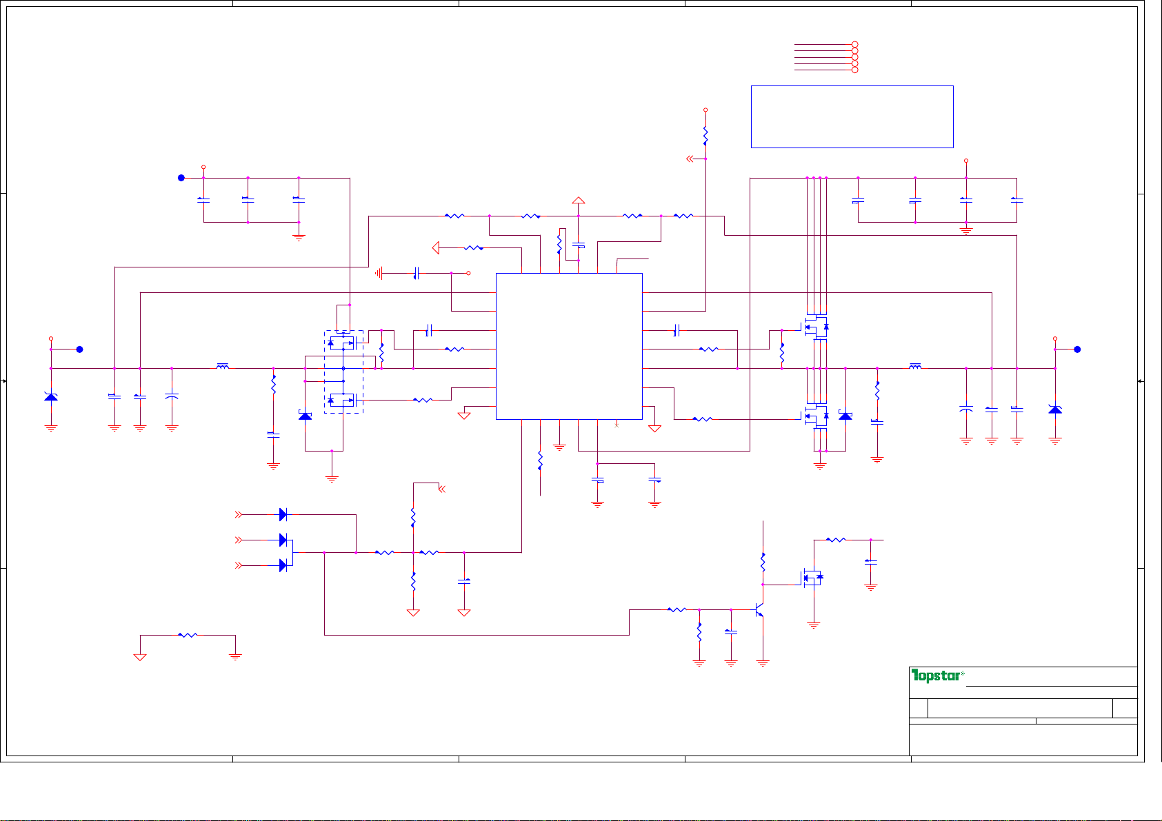
5
4
3
2
+V3.3AL 12,14,15,16,18,19,21,23,25,26,27,28,30,31,32,33,35
+VDC 12,19,21,27,30,31,32,33,34,35
AD+ 27,33
+V5AL 12,16,21,30,31,32,33
EC_RTC 15
1
D D
2
VFB1
17
VREG5
PC194
PC194
4.7uF/10V,X5R
4.7uF/10V,X5R
C0805
C0805
ALW_PWROK25
PR51
PR51
10K,1% R0402
10K,1% R0402
ENTRIP1
1
24
VO1
ENTRIP1
23
PGOOD
22
VBST1
21
DRVH1
20
LL1
19
DRVL1
G1
GND1
VCLK
18
GND_TPS51125
+VDC
VDC2
VDC2
TestP
TestP
TPC60
TPC60
ns
ns
C C
+V3.3AL
V3.3AL
V3.3AL
TestP
TestP
TPC60
TPC60
5A
ns
ns
12
PC241
PC241
1
1
C1206
C1206
PC245
PC245
+
+
220UF/6.3V,OSCON
PZ16
PZ16
BZT52C3V6S-F/3.6
BZT52C3V6S-F/3.6
SOD323
SOD323
1 2
ns
ns
PC147
PC147
1000pF/50V,X7R
1000pF/50V,X7R
C0402
C0402
Update PC245 to 533115722001 for Buyer request
B B
A A
090917
GND_TPS51125
5
220UF/6.3V,OSCON
CAP6_6x7_3
CAP6_6x7_3
4.7uF/25V,X7R
4.7uF/25V,X7R
PR251 0
PR251 0
2A 2A
T
PC189
1N5819
1N5819
PD10
PD10
1N4148WS
1N4148WS
SOD323
SOD323
1
1
PD12
PD12
BAT54C
BAT54C
SOT23
SOT23
SO8_50_150
SO8_50_150
PD32
PD32
SOD123
SOD123
ns
ns
PC189
1000pF/50V,X7R
1000pF/50V,X7R
C0402
C0402
PQ75
PQ75
AO4932
AO4932
7
6
1
1
3
1
D1 D1
D1 D1
S1
S1
D2
D2
S2 G2
S2 G2
4
3A
2
8
G1
G1
5
3
PR255 0 R0402
PR255 0 R0402
4
GND_TPS51125
PC193
PC193
PR250
PR250
10K
10K
R0402
R0402
PR247 0
PR247 0
R0402
R0402
ns
ns
GND_TPS51125
10uF/6.3V,X5R
10uF/6.3V,X5R
C0805
C0805
PR99
PR99
100K
100K
R0402
R0402
PC211
PC211
10uF/ 25V
10uF/ 25V
C1210
C1210
PL13
PL13
3.3uH/4.8A
3.3uH/4.8A
LS2_8836
LS2_8836
PWR_SW_VCC219,21
ALWAYS_ON25
ALW_EN27
R0402
R0402
1
1
PC244
PC244
0.1uF/25V,X7R
0.1uF/25V,X7R
C0603
C0603
PR260
PR260
2.2
2.2
R0805
R0805
ns
ns
PC153
PC153
1000pF/50V,X7R
1000pF/50V,X7R
C0402
C0402
ns
ns
2
1
PR252 5.11K,1%PR252 5.11K,1%
PC253
PC253
0.1uF/25V,X7R
0.1uF/25V,X7R
PR246
PR246
C0603
C0603
4.7
4.7
GND_TPS51125
Isense_SYSN
PR58
PR58
510K
510K
R0402
R0402
PR209
PR209
1K
1K
R0402
R0402
GND_TPS51125
PR272
PR272
100K
100K
R0402
R0402
EC_RTC
7
8
9
10
11
12
G2
PC57
PC57
0.022uF/16V,X7R
0.022uF/16V,X7R
C0402
C0402
ns
ns
PR56 7.68K,1%PR56 7.68K,1%
ENTRIP1
VO2
VREG3
VBST2
DRVH2
LL2
DRVL2
GND2
{43}
GND_TPS51125
PR248
PR248
0
0
4
5
6
VFB2
TONSEL
ENTRIP2
PU9
PU9
RT8205B
RT8205B
S_Top
S_Top
EN0
SKIPSEL14GND15VIN16VREG5
13
PR254
PR254
0
0
R0402
R0402
VREF
PC78
PC78
0.22uF/16V,X7R
0.22uF/16V,X7R
C0603
C0603
R0402
R0402
VREF
3
VREF
3
ns
ns
+V3.3AL
PR203
PR203
15K,1%
15K,1%
R0402
R0402
PC252
PC252
0.1uF/25V,X7R
0.1uF/25V,X7R
C0603
C0603
PR249 0
PR249 0
PC195
PC195
10uF/6.3V,X5R
10uF/6.3V,X5R
C0805
C0805
PR204
PR204
1K
1K
R0402
R0402
PR231
PR231
30K
30K
R0402
R0402
PR240
PR240
4.7
4.7
R0402
R0402
0.1uF/25V,Y5V
0.1uF/25V,Y5V
1.输入电容要靠近MOSFET漏极
2.MOS管尽量靠近IC芯片
3.芯片的Thermal
GND用至少5个过孔连到信号地,用来散热
PR253
PR253
51K
51K
4.信号地和电源地在输出电容的负极连到一起
R0402
R0402
S_Top
S_Top
10K
10K
R0402
R0402
PQ86
PQ86
AO4468
AO4468
567
D
D
4
G
G
S
S
567
D
D
4
G
G
S
S
PQ85
PQ85
AO4468
AO4468
SO8_50_150
SO8_50_150
PR243
PR243
SO8_50_150
SO8_50_150
5A
VREG5
PR207
PR207
3
47K
47K
R0402
R0402
S_Top
S_Top
PQ81
PQ81
MMBT3904-F
MMBT3904-F
2 3
1
2
2
PC146
PC146
C0402
C0402
ns
ns
1
8
123
LL2
8
123
PR232
PR232
1K
1K
R0402
R0402
PQ84
PQ84
2N7002
2N7002
SOT23
SOT23
1
1
PD33
PD33
1N5819
1N5819
SOD123
SOD123
S_Top
S_Top
ENTRIP1
PC243
PC243
1000pF/50V,X7R
1000pF/50V,X7R
C0402
C0402
PR261
PR261
2.2
2.2
R0805
R0805
ns
ns
PC144
PC144
1000pF/50V,X7R
1000pF/50V,X7R
C0402
C0402
ns
ns
PC154
PC154
0.1uF/25V,Y5V
0.1uF/25V,Y5V
C0402
C0402
ns
ns
+VDC
PC242
1
1
PC190
PC190
CAP6_6x7_3
CAP6_6x7_3
PC190
PC242
10uF/ 25V,X7R
10uF/ 25V,X7R
C1210
C1210
12
+
+
4.2
090723
PC188
PC188
0.1uF/25V,X7R
0.1uF/25V,X7R
C0603
C0603
PL17
PL17
5.2uH/5.5A
5.2uH/5.5A
LS2_1051
LS2_1051
S_Bot
S_Bot
1
1
220UF/6.3V,OSCON
220UF/6.3V,OSCON
Page Name
Page Name
Page Name
Size
Size
Size
Project Name Rev
Project Name Rev
Project Name Rev
Custom
Custom
Custom
Date: Sheet
Date: Sheet
Date: Sheet
PROPERTY NOTE: this document contains information confidential and property to
PROPERTY NOTE: this document contains information confidential and property to
PROPERTY NOTE: this document contains information confidential and property to
TOPSTAR and shall not be reproduced or transferred to other documents or disclosed
TOPSTAR and shall not be reproduced or transferred to other documents or disclosed
TOPSTAR and shall not be reproduced or transferred to other documents or disclosed
to others or used for any purpose other than that for which it was obtained without
to others or used for any purpose other than that for which it was obtained without
to others or used for any purpose other than that for which it was obtained without
the expressed written consent of TOPSTAR
the expressed written consent of TOPSTAR
the expressed written consent of TOPSTAR
PC239
PC239
4.7uF/25V,X7R
4.7uF/25V,X7R
C1206
C1206
PC139
PC139
1000pF/50V,X7R
1000pF/50V,X7R
C0402
C0402
TOPSTAR TECHNOLOGY
TOPSTAR TECHNOLOGY
TOPSTAR TECHNOLOGY
Liu JX
Liu JX
Liu JX
+V3.3AL/+V5AL
+V3.3AL/+V5AL
+V3.3AL/+V5AL
P01
P01
P01
PC143
PC143
4.7uF/25V,X7R
4.7uF/25V,X7R
C1206
C1206
+V5AL
5A
1
V5AL
V5AL
PZ17
PZ17
BZT52C5V6S-F/5.6
BZT52C5V6S-F/5.6
SOD323
SOD323
ns
ns
1 2
29 39Thursday, April 29, 2010
29 39Thursday, April 29, 2010
29 39Thursday, April 29, 2010
TestP
TestP
TPC60
TPC60
ns
ns
of
of
of
A
A
A
Page 30
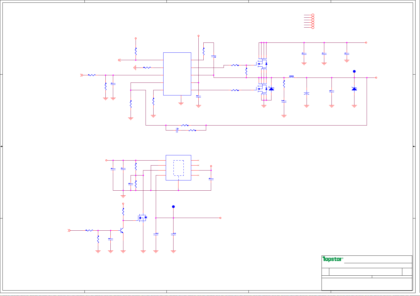
5
D D
DDR3_DRAM_PWROK8,25,32
PR195 1K
V1_5_ON25
C C
B B
PR195 1K
R0402
R0402
0.1UF/10V,X7R
0.1UF/10V,X7R
PR940
PR940
100K
100K
R0402
R0402
+V1.5
PC64
PC64
C0402
C0402
4
PC59
PC59
0.022uF/16V,X7R
0.022uF/16V,X7R
C0402
C0402
ns
ns
2A
PC66
PC66
C0805
C0805
4.7uF/10V,X5R
4.7uF/10V,X5R
PC67
PC67
0.1UF/10V,X7R
0.1UF/10V,X7R
C0402
C0402
+V3.3AL
PR80
PR80
10K,1%
10K,1%
PR194
PR194
1K
1K
R0402
R0402
S_Top
S_Top
R940 130K
R940 130K
PR98
PR98
10K,1%
10K,1%
PR100
PR100
10K,1%
10K,1%
R0402
R0402
PR86
PR86
470K
470K
Set Fsw 290K
tps51218
tps51218
PU10
PU10
1
PGOOD
2
TRIP
3
EN
4
VFB
5
RF
PU7
PU7
AP1250
AP1250
SOP8_1D27_4G
SOP8_1D27_4G
1
VIN
2
GND
3
REFEN
4
VOUT
TPS51218
TPS51218
GND
11
PR263
PR263
11.5K,1%
11.5K,1%
PC60
PC60
0.022uF/16V,X7R
0.022uF/16V,X7R
ns
ns
C0402
C0402
VCNTL
PGND
9
VBST
DRVH
V5IN
DRVL
NC3
NC2
NC1
SW
PR68
PR68
20K
20K
R0402
R0402
10
9
8
7
6
8
7
6
5
+V5AL
PC72
PC72
4.7uF/10V,X5R
4.7uF/10V,X5R
C0805
C0805
ns
ns
3
PR193
PR193
0
0
R0402
R0402
+V3.3AL
PC248
PC248
0.1uF/25V,X7R
0.1uF/25V,X7R
C0603
C0603
Update PD13 to 1N5819 for EMI request
PC65
PC65
4.7uF/10V,X5R
4.7uF/10V,X5R
C0805
C0805
PR201
PR201
R0402
R0402
PR200
PR200
0
0
R0402
R0402
090917
0
0
4
PR50
PR50
10K
10K
4
PQ54
PQ54
AO4468
AO4468
SO8_50_150
SO8_50_150
D
D
G
G
D
D
G
G
567
S
S
567
S
S
8
AO4468
AO4468
PQ53
PQ53
SO8_50_150
SO8_50_150
123
8
1
1
123
PD25
PD25
SSM34PT
SSM34PT
SMA
SMA
2
PL7
PL7
2.2UH/14A
2.2UH/14A
LS2_6530
LS2_6530
1
1
PR262
PR262
2.2
2.2
R0805
R0805
ns
ns
PC135
PC135
1000pF/50V,X7R
1000pF/50V,X7R
C0402
C0402
ns
ns
1
+V0.75S 13,34
+V5AL 12,16,21,29,31,32,33
+V3.3AL 12,14,15,16,18,19,21,23,25,26,27,28,29,31,32,33,35
+VDC 12,19,21,27,29,31,32,33,34,35
+V1.5 8,10,13,32,33,34
+V3.3S 6,7,9,10,11,12,13,14,15,16,17,19,21,22,23,24,25,26,31,32,33,34,35
PC56
PC56
4.7uF/25V,X7R
TPC60
TPC60
4.7uF/25V,X7R
C1206
C1206
V1_5
V1_5
TestP
TestP
ns
ns
PC61
PC61
1000pF/50V,X7R
PC62
PC62
0.1uF/25V,X7R
0.1uF/25V,X7R
C0603
C0603
1000pF/50V,X7R
C0402
C0402
5A 5A
PC63
PC63
C0402
C0402
0.1uF/10V,X7R
12
1
1
+
+
PC136
PC136
220UF/6.3V,OSCON
220UF/6.3V,OSCON
CAP6_6x7_3
CAP6_6x7_3
0.1uF/10V,X7R
+VDC
PZ2
PZ2
BZT52C2V0S-F/2.0V
BZT52C2V0S-F/2.0V
SOD323
SOD323
1 2
ns
ns
2A
+V1.5
+V3.3AL
PR106
PR106
3
47K
47K
R0402
R0402
PR112
PR112
1K
1K
R0402
R0402
V0_75S_ON25
PR110
PR110
30K
30K
R0402
R0402
A A
5
1
PC76
PC76
C0402
C0402
0.1UF/10V,X5R
0.1UF/10V,X5R
ns
ns
PQ24
PQ24
MMBT3904-F
MMBT3904-F
2 3
4
1
PQ22
PQ22
2N7002
2N7002
SOT23
SOT23
2
PC70
PC70
10uF/6.3V,X5R
10uF/6.3V,X5R
C0805
C0805
ns
ns
V0_75S
V0_75S
ns
ns
TestP
TestP
TPC60
TPC60
PC69
PC69
10uF/6.3V,X5R
10uF/6.3V,X5R
C0805
C0805
+V0.75S
2A
TOPSTAR TECHNOLOGY
TOPSTAR TECHNOLOGY
TOPSTAR TECHNOLOGY
Liu JX
Liu JX
Page Name
Page Name
Page Name
Size
Size
Size
Project Name Rev
Project Name Rev
Project Name Rev
A3
A3
A3
Date: Sheet
Date: Sheet
Date: Sheet
PROPERTY NOTE: this document contains information confidential and property to
PROPERTY NOTE: this document contains information confidential and property to
PROPERTY NOTE: this document contains information confidential and property to
TOPSTAR and shall not be reproduced or transferred to other documents or disclosed
TOPSTAR and shall not be reproduced or transferred to other documents or disclosed
TOPSTAR and shall not be reproduced or transferred to other documents or disclosed
to others or used for any purpose other than that for which it was obtained without
to others or used for any purpose other than that for which it was obtained without
to others or used for any purpose other than that for which it was obtained without
the expressed written consent of TOPSTAR
the expressed written consent of TOPSTAR
3
2
the expressed written consent of TOPSTAR
Liu JX
+V1.5/+V0.75S DDR
+V1.5/+V0.75S DDR
+V1.5/+V0.75S DDR
P02
P02
P02
1
30 39Friday, April 30, 2010
30 39Friday, April 30, 2010
30 39Friday, April 30, 2010
Mayc
A
A
A
of
of
of
Page 31
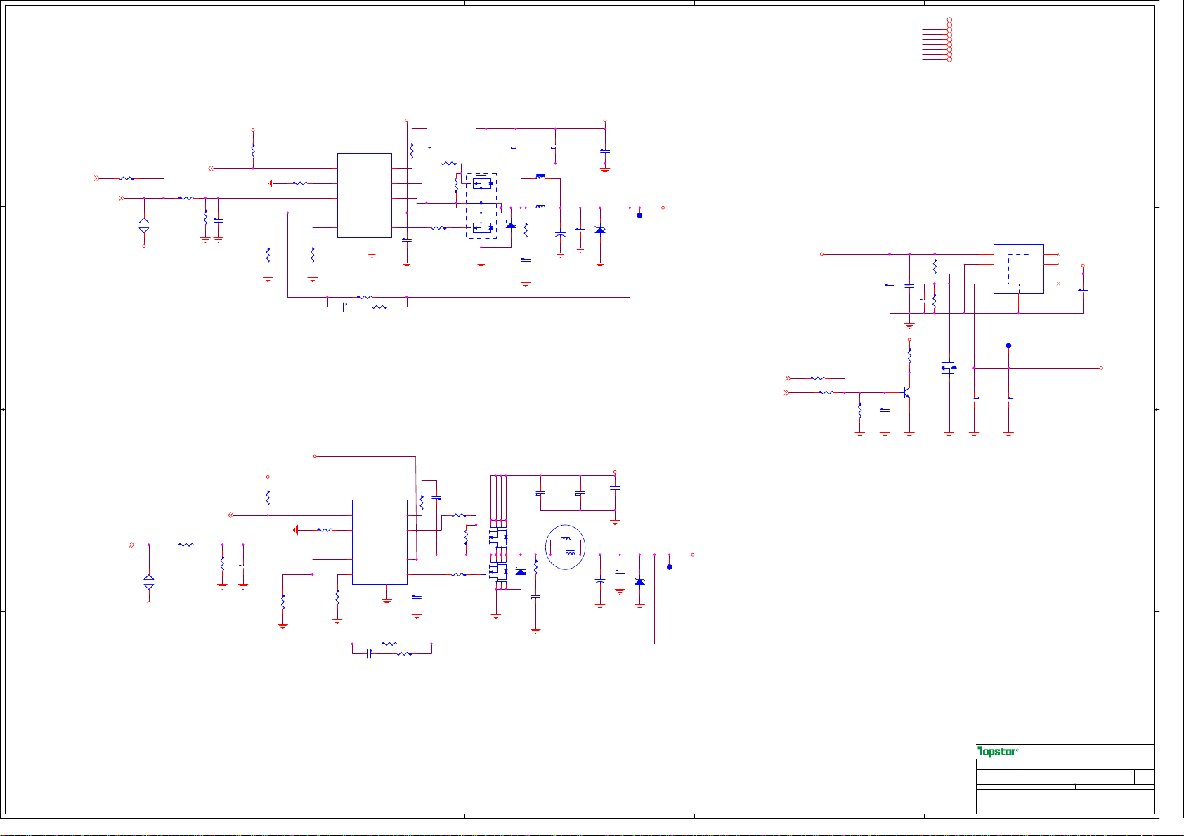
5
4
3
2
+V3.3AL 12,14,15,16,18,19,21,23,25,26,27,28,29,30,32,33,35
+V3.3S 6,7,9,10,11,12,13,14,15,16,17,19,21,22,23,24,25,26,32,33,34,35
+VDC 12,19,21,27,29,30,32,33,34,35
+V1.5S 10,14,16,19,23,33,34
+V1.05S 6,7,10,15,16,24,32,34
+V5AL 12,16,21,29,30,32,33
+V0.89S 10,34
+V1.8S 10,32
+V5S 11,12,16,17,21,22,23,25,33,34,35
1
D D
+V3.3S
PR89
PR89
47K
47K
R0402
R0402
ns
PC73
PC73
0.022uF/16V,X7R
0.022uF/16V,X7R
C0402
C0402
ns
ns
PR79
PR79
10K,1%
10K,1%
R0402
R0402
ns
+V3.3S
PC123
PC123
0.022uF/16V,X7R
0.022uF/16V,X7R
C0402
C0402
ns
ns
PR264 100K,1%
PR264 100K,1%
PR90
PR90
47K
47K
R0402
R0402
S_Top
S_Top
PR87
PR87
10K,1%
10K,1%
R0402
R0402
nsPR236
ns
+V3.3AL
12
+V3.3AL
J7
J7
JOPEN
JOPEN
RESISTOR_1
RESISTOR_1
ns
ns
12
J8
J8
JOPEN
JOPEN
RESISTOR_1
RESISTOR_1
ns
ns
+V0.89SPWROK32
PR234
PR234
1K
1K
R0402
R0402
PR942
PR942
100K
100K
R0402
R0402
+V1.05SPWROK32
PR197
PR197
PR943
PR943
1K
1K
100K
100K
R0402
R0402
R0402
R0402
+V1.05SPWROK32
C C
B B
PR236
0 R0402
0 R0402
V0_89S_ON25
V1_05S_ON25
PU14
PU14
TPS51218
TPS51218
1
PGOOD
2
TRIP
R0402
R0402
3
EN
4
VFB
5
RF
tps51218
tps51218
PR266
PR266
470K
470K
R0402
R0402
PR57
PR57
2.74K,1%
2.74K,1%
PC42
PC42
0.022uF/16V,X7R
0.022uF/16V,X7R
ns
ns
C0402
C0402
+V5S
PU3
PU3
1
PGOOD
PR267
PR267
130K
130K
2
TRIP
R0402
R0402
3
EN
4
VFB
5
RF
PR268
PR268
tps51218
tps51218
470K
470K
R0402
R0402
VBST
DRVH
SW
V5IN
DRVL
GND
11
PR53
PR53
20K
20K
R0402
R0402
TPS51218
TPS51218
GND
11
PR69
PR69
5.11K,1%
5.11K,1%
R0402
R0402
ns
ns
DRVH
VBST
DRVL
10
9
8
7
6
V5IN
SW
+V5S
PR190
PR190
0
0
R0402
R0402
PC49
PC49
4.7uF/10V,X5R
4.7uF/10V,X5R
C0805
C0805
PR187
PR187
R0402
R0402
10
9
8
7
6
PC79
PC79
4.7uF/10V,X5R
4.7uF/10V,X5R
C0805
C0805
PC249
PC249
0.1uF/25V,X7R
0.1uF/25V,X7R
C0603
C0603
PR189
PR189
R0402
R0402
PR257
PR257
10K
10K
R0402
R0402
PR183
PR183
0
0
R0402
R0402
PC250
PC250
0.1uF/25V,X7R
0.1uF/25V,X7R
C0603
C0603
0
0
1.5A
PC51
PC51
1000pF/50V,X7R
0
0
2
8
G1
G1
5
3
PR198
PR198
0
0
R0402
R0402
PR258
PR258
4
10K
10K
R0402
R0402
PR237
PR237
0
0
R0402
R0402
4
PQ70
PQ70
AO4468
AO4468
SO8_50_150
SO8_50_150
1000pF/50V,X7R
C0402
C0402
1
D1D1
D1D1
PQ6
S1
S1
D2
D2
S2G2
S2G2
4
0.01uF/25V,X7R
0.01uF/25V,X7R
567
D
D
G
G
S
S
567
D
D
G
G
S
S
PQ6
AO4932
AO4932
SO8_50_150
SO8_50_150
7
6
3.3uH/4.8A
3.3uH/4.8A
1
1
PL6
LS2_8836
PL6
LS2_8836
PL15
PL15
2.2UH/14A
2.2UH/14A
LS2_6530
LS2_6530
1
1
ns
ns
1
1
PD30
PD30
PR265
PR265
1N5819
1N5819
2.2
2.2
SOD123
SOD123
R0805
R0805
ns
ns
ns
ns
PC127
PC127
C0402
C0402
ns
ns
PC138
PC138
220UF/6.3V,OSCON
220UF/6.3V,OSCON
CAP6_6x7_3
CAP6_6x7_3
Update PC138 to 533115722001 for Buyer request
090917
PC77
PC77
1000pF/50V,X7R
1000pF/50V,X7R
C0402
C0402
8
PQ68
PQ68
AO4468
AO4468
SO8_50_150
SO8_50_150
123
8
PD31
PD31
1N5819
1N5819
SOD123
SOD123
123
R938
R938
2.2
2.2
R0805
R0805
1
1
ns
ns
PC74
PC74
1000pF/50V,X7R
1000pF/50V,X7R
C0402
C0402
ns
ns
PL11
PL11
2.2UH/14A
2.2UH/14A
LS2_6530 ns
LS2_6530 ns
+VDC
PC53
PC53
0.1uF/25V,X7R
0.1uF/25V,X7R
C0603
C0603
080716VA:Co_lay.
12
1
1
+
+
1 2
PC126
PC126
0.1uF/10V,X5R
0.1uF/10V,X5R
C0402
C0402
1.5A
PC137
PC137
0.1uF/25V,X7R
0.1uF/25V,X7R
C0603
C0603
080716VA:Co_lay.
1
1
1
1
PL5
PL5
3.3uH/4.8A
3.3uH/4.8A
LS2_8836
LS2_8836
12
1
1
+
+
PC140
PC140
220UF/6.3V,OSCON
220UF/6.3V,OSCON
CAP6_6x7_3
CAP6_6x7_3
PC68
PC68
C1206
C1206
4.7uF/25V,X7R
4.7uF/25V,X7R
2A
V0_89S
V0_89S
TestP
TestP
TPC60
TPC60
PD23
PD23
ns
ns
SOD323
SOD323
BZT52C2V0S-F/2.0V
BZT52C2V0S-F/2.0V
ns
ns
+VDC
PC131
PC131
4.7uF/25V,X7R
4.7uF/25V,X7R
C1206
C1206
PC124
PC124
0.1uF/10V,X5R
0.1uF/10V,X5R
C0402
C0402
PD24
PD24
ns
ns
1 2
SOD323
SOD323
BZT52C2V0S-F/2.0V
BZT52C2V0S-F/2.0V
+V0.89S
V1_05S
V1_05S
TestP
TestP
TPC60
TPC60
PU11
PU11
AP1250
AP1250
SOP8_1D27_4G
PQ83
PQ83
L2N7002LT1G
L2N7002LT1G
SOT23
SOT23
SOP8_1D27_4G
1
VIN
2
GND
3
REFEN
VOUT4NC1
PC50
PC50
10uF/6.3V,X5R
10uF/6.3V,X5R
C0805
C0805
ns
ns
PGND
9
TPC60
TPC60
TestP
TestP
V1_8S
V1_8S
ns
ns
PC52
PC52
10uF/6.3V,X5R
10uF/6.3V,X5R
C0805
C0805
VCNTL
8
NC3
+V3.3AL
7
NC2
6
5
PC75
PC75
4.7uF/10V,X5R
4.7uF/10V,X5R
C0805
C0805
2A
+V1.8S
PC45
PC45
4.7uF/10V,X5R
4.7uF/10V,X5R
C0805
C0805
0.1UF/10V,X7R
0.1UF/10V,X7R
+V3.3AL
1
PR226
PR226
10K,1%
10K,1%
R0402
R0402
PC71
PC71
C0402
C0402
PQ80
PQ80
MMBT3904-F
MMBT3904-F
2 3
2A
PR224
PR224
47K
47K
R0402
R0402
S_Bot
S_Bot
PR228
PR228
12.1K,1%
12.1K,1%
3
1
2
+V3.3S
PC55
PC55
0.1UF/10V,X7R
0.1UF/10V,X7R
C0402
C0402
PR256 0
PR256 0
R0402
V1.8S_ON25
+V1.05SPWROK32
+V1.05S
4A
ns
ns
PR227
PR227
R0402
R0402
R0402
ns
ns
1K
1K
PR225
PR225
30K
30K
R0402
R0402
PC152
PC152
0.1UF/10V,X5R
0.1UF/10V,X5R
C0402
C0402
ns
ns
PC41
PC41
0.022uF/16V,X7R
0.022uF/16V,X7R
C0402
C0402
A A
5
4
PR43
PR43
20K
20K
R0402
R0402
ns
ns
ns
ns
TOPSTAR TECHNOLOGY
TOPSTAR TECHNOLOGY
TOPSTAR TECHNOLOGY
Page Name
Page Name
Page Name
Size
Size
Size
Project Name Rev
Project Name Rev
Project Name Rev
A2
A2
A2
Date: Sheet
Date: Sheet
Date: Sheet of
PROPERTY NOTE: this document contains information confidential and property to
PROPERTY NOTE: this document contains information confidential and property to
PROPERTY NOTE: this document contains information confidential and property to
TOPSTAR and shall not be reproduced or transferred to other documents or disclosed
TOPSTAR and shall not be reproduced or transferred to other documents or disclosed
TOPSTAR and shall not be reproduced or transferred to other documents or disclosed
to others or used for any purpose other than that for which it was obtained without
to others or used for any purpose other than that for which it was obtained without
to others or used for any purpose other than that for which it was obtained without
the expressed written consent of TOPSTAR
the expressed written consent of TOPSTAR
3
2
the expressed written consent of TOPSTAR
1
1.8S 1.05S 0.89S
1.8S 1.05S 0.89S
1.8S 1.05S 0.89S
P02
P02
P02
mayc
A
A
A
31 39Friday, April 30, 2010
31 39Friday, April 30, 2010
31 39Friday, April 30, 2010
of
of
Page 32
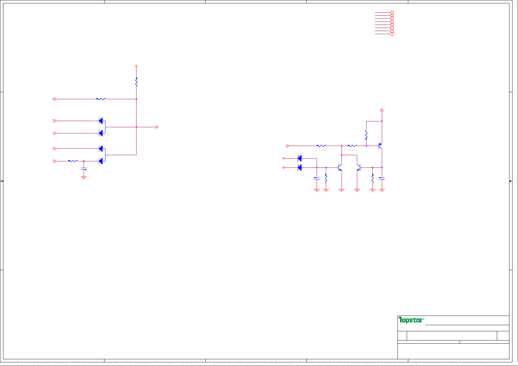
5
Power Good Logic CIRCUIT
D D
4
3
2
+V3.3S 6,7,9,10,11,12,13,14,15,16,17,19,21,22,23,24,25,26,31,33,34,35
+V5AL 12,16,21,29,30,31,33
+V3.3AL 12,14,15,16,18,19,21,23,25,26,27,28,29,30,31,33,35
+V1.05S 6,7,10,15,16,24,31,34
+V1.8S 10,31
+VCC_CORE 10,35
+V1.5 8,10,13,30,33,34
+VDC 12,19,21,27,29,30,31,33,34,35
1
+V3.3S
PR130
PR130
47K
47K
R0402
R0402
S_Top
PR81
PR81
1K
1K
R0402
+V0.89SPWROK31
R0402
S_Top
SHDN#27,28
+V1.05SPWROK31
C C
B B
DDR3_DRAM_PWROK8,25,30
PM_RSMRST#15,25
PM_SLP_S3#15,25
PR128
PR128
1K
1K
R0402
R0402
1
2
1
2
PC88
PC88
0.1uF/10V,X7R
0.1uF/10V,X7R
C0402
C0402
3
PD11
PD11
BAT54A
BAT54A
SOT23
SOT23
3
PD13
PD13
BAT54A
BAT54A
SOT23
SOT23
MAIN_PWROK 25
PR320
PR320
51K
PQ112
PQ112
MMBT3904-F
MMBT3904-F
SOT23
SOT23
1
2 3
PR313
PR313
20K
20K
R0402
R0402
51K
R0402
R0402
1
PQ69
PQ69
23
MMBT2907
MMBT2907
SOT23
SOT23
PC217
PC217
0.1uF/16V,X7R
0.1uF/16V,X7R
C0402
C0402
PR323
PR323
100
100
R0402
PR307 0
PR307 0
R0402
SHDN_LOCK#24
+V5AL
+V3.3AL
PZ9
PZ9
BZT52C5V6S-F/5.6
BZT52C5V6S-F/5.6
SOD323
SOD323
12
12
PZ8
PZ8
BZT52C3V6S-F/3.6
BZT52C3V6S-F/3.6
SOD323
SOD323
PC203
PC203
1uF/10V,X7R
1uF/10V,X7R
C0603
C0603
R0402
PQ66
PQ66
MMBT3904-F
MMBT3904-F
SOT23
SOT23
PR304
PR304
100
100
R0402
R0402
R0402
1
2 3
A A
Page Name
Page Name
Page Name
Size
Size
Size
Project Name Rev
Project Name Rev
Project Name Rev
A3
A3
A3
Date: Sheet
Date: Sheet
Date: Sheet
PROPERTY NOTE: this document contains information confidential and property to
PROPERTY NOTE: this document contains information confidential and property to
PROPERTY NOTE: this document contains information confidential and property to
TOPSTAR and shall not be reproduced or transferred to other documents or disclosed
TOPSTAR and shall not be reproduced or transferred to other documents or disclosed
TOPSTAR and shall not be reproduced or transferred to other documents or disclosed
to others or used for any purpose other than that for which it was obtained without
to others or used for any purpose other than that for which it was obtained without
to others or used for any purpose other than that for which it was obtained without
the expressed written consent of TOPSTAR
the expressed written consent of TOPSTAR
5
4
3
2
the expressed written consent of TOPSTAR
TOPSTAR TECHNOLOGY
TOPSTAR TECHNOLOGY
TOPSTAR TECHNOLOGY
Liu JX
Liu JX
Liu JX
Power Good logic/OVP
Power Good logic/OVP
Power Good logic/OVP
P02
P02
P02
1
A
A
32 39Thursday, April 29, 2010
32 39Thursday, April 29, 2010
32 39Thursday, April 29, 2010
A
of
of
of
Page 33

+VDC
MAIN_PWR_DN
34
MAIN_ON25
PR278
PR278
1K
1K
R0402
R0402
PR205
PR205
510K
510K
R0402
R0402
+VDC 12,19,21,27,29,30,31,32,34,35
+V5S 11,12,16,17,21,22,23,25,31,34,35
+V3.3S 6,7,9,10,11,12,13,14,15,16,17,19,21,22,23,24,25,26,31,32,34,35
+V5AL 12,16,21,29,30,31,32
+V3.3AL 12,14,15,16,18,19,21,23,25,26,27,28,29,30,31,32,35
+V1.5S 10,14,16,19,23,34
+V1.5 8,10,13,30,32,34
AD+ 27
BATT+ 27,28,36
4
PQ52
PQ52
+V3.3AL
567
8
D
D
G
G
S
S
123
PC166
PC166
1uF/10V,X7R
1uF/10V,X7R
C0603
C0603
V3_3S1
V3_3S1
TestP
TestP
TPC60
TPC60
ns
ns
4A
+V3.3S
PR274
PR274
1K
1K
R0402
2 3
PQ50
PQ50
DTB114EK
DTB114EK
SOT23
PR172
PR172
PC162
PC162
100K
100K
0.01uF/25V,X7R
0.01uF/25V,X7R
R0402
R0402
C0402
C0402
PR206
PR206
1K
1K
R0402
R0402
3
PQ51
PQ51
2N7002
1
2N7002
SOT23
SOT23
2
SOT23
1
R0402
PR208
PR208
100K
100K
R0402
R0402
PR245
PR245
51K
51K
R0402
R0402
567
D
D
4
G
G
S
S
AO4468
AO4468
PQ55
PQ55
SO8_50_150
SO8_50_150
PC80
PC80
0.1uF/25V,X7R
0.1uF/25V,X7R
C0603
C0603
+V5AL
8
123
PC179
PC179
1uF/10V,X7R
1uF/10V,X7R
C0603
C0603
V5S1
V5S1
TestP
TestP
TPC60
TPC60
ns
ns
+V5S
PR275
PR275
0
0
R0402
R0402
PR173
PR173
33K
33K
R0402
R0402
PD27
PD27
1N4148WS
1N4148WS
SOD323
SOD323
1
1
PR276
PR276
51K
51K
R0402
R0402
+V1.5
AO4468
AO4468
SO8_50_150
SO8_50_150
PC81
PC81
0.1uF/25V,X7R
0.1uF/25V,X7R
C0603
C0603
PD34
PR141
PR141
100K
100K
R0402
+VDC
PR273
PR273
100K
100K
R0402
R0402
ns
ns
PQ18
V1_5S_ON25
PR277 20K
R0402
R0402
nsPR277 20K
ns
PR244
PR244
100K
100K
R0402
R0402
ns
ns
1
PQ18
MMBT3904-F
MMBT3904-F
SOT23
SOT23
ns
ns
2 3
R0402
PQ65
PQ65
2N7002
2N7002
SOT23
SOT23
ns
ns
1
PR241
PR241
100K
100K
R0402
R0402
ns
ns
PD34
1N4148WS
1N4148WS
1
1
SOD323
SOD323
3
PC149
PC149
0.1UF/25V,X7R
0.1UF/25V,X7R
C0603
C0603
2
D
D
4
G
G
AO4468
AO4468
PQ34
PQ34
SO8_50_150
SO8_50_150
567
S
S
8
123
PC148
PC148
1uF/10V,X7R
1uF/10V,X7R
C0603
C0603
V1_5S
V1_5S
TestP
TestP
TPC80 ns
2A
TPC80 ns
+V1.5S
TOPSTAR TECHNOLOGY
TOPSTAR TECHNOLOGY
TOPSTAR TECHNOLOGY
Liu JX
Liu JX
Page Name
Page Name
Page Name
Size
Size
Size
Project Name Rev
Project Name Rev
Project Name Rev
A3
A3
A3
Date: Sheet
Date: Sheet of
Date: Sheet of
PROPERTY NOTE: this document contains information confidential and property to
PROPERTY NOTE: this document contains information confidential and property to
PROPERTY NOTE: this document contains information confidential and property to
TOPSTAR and shall not be reproduced or transferred to other documents or disclosed
TOPSTAR and shall not be reproduced or transferred to other documents or disclosed
TOPSTAR and shall not be reproduced or transferred to other documents or disclosed
to others or used for any purpose other than that for which it was obtained without
to others or used for any purpose other than that for which it was obtained without
to others or used for any purpose other than that for which it was obtained without
the expressed written consent of TOPSTAR
the expressed written consent of TOPSTAR
the expressed written consent of TOPSTAR
Liu JX
V5S/ V3.3S/ V1.5S Power
V5S/ V3.3S/ V1.5S Power
V5S/ V3.3S/ V1.5S Power
P02
P02
P02
A
A
A
of
33 39Thursday, April 29, 2010
33 39Thursday, April 29, 2010
33 39Thursday, April 29, 2010
Page 34
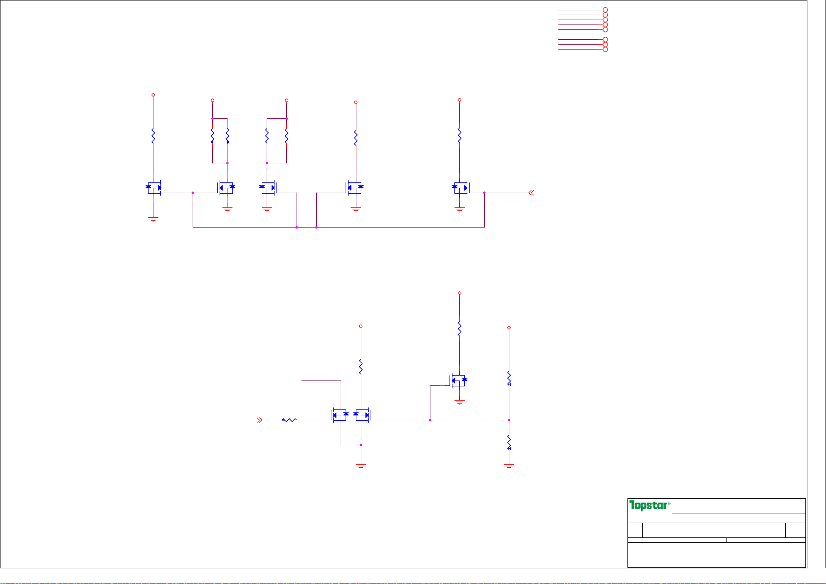
+V3.3S 6,7,9,10,11,12,13,14,15,16,17,19,21,22,23,24,25,26,31,32,33,35
+V1.05S 6,7,10,15,16,24,31,32
+V1.5S 10,14,16,19,23,33
+V1.5 8,10,13,30,32,33
+V0.75S 13,30
+VDC 12,19,21,27,29,30,31,32,33,35
+V5S 11,12,16,17,21,22,23,25,31,33,35
+V0.89S 10,31
PR217
PR217
100
100
R0402
R0402
30mA
+V1.5S
PQ63
PQ63
2N7002
2N7002
SOT23
SOT23
1
+V0.89S
1 2
3
2
+V0.75S
1 2
3
2
PR214
PR214
100
100
R0402
R0402
PR212
PR212
100
100
R0402
R0402
PQ64
PQ64
2N7002
2N7002
SOT23
SOT23
1
+VDC
PR219
PR219
510K
510K
R0402
R0402
PR211
PR211
200K
200K
R0402
R0402
MAIN_PWR_DN
33
+V3.3S+V5S
PR168
PR168
100
100
R0402
R0402
70mA
1 2
3
2
1 2
PQ41
PQ41
2N7002
2N7002
SOT23
SOT23
1
PR169
PR169
100
100
R0402
R0402
10KPR210
10KPR210
R0402
R0402
V1_5DISCHG
PQ62
PQ62
2N7002
2N7002
SOT23
SOT23
1
100mA
PR171
PR170
PR170
100
100
R0402
PQ61
PQ61
SOT23
SOT23
R0402
PQ42
PQ42
2N7002
2N7002
SOT23
SOT23
1 2
3
2N7002
2N7002
1
2
PR171
100
100
R0402
R0402
3
1
2
PM_SLP_S4#15,25
+V1.05S
PR222
PR222
100
100
R0402
R0402
1 2
3
PQ60
PQ60
2N7002
2N7002
SOT23
1
SOT23
2
+V1.5
PR221
PR221
100
100
R0402
R0402
1 2
PQ59
PQ59
3
3
2
2N7002
2N7002
SOT23
SOT23
V1_5DISCHG
1
2
TOPSTAR TECHNOLOGY
TOPSTAR TECHNOLOGY
TOPSTAR TECHNOLOGY
Liu JX
Liu JX
Page Name
Page Name
Page Name
Size
Size
Size
Project Name Rev
Project Name Rev
Project Name Rev
A3
A3
A3
Date: Sheet
Date: Sheet of
Date: Sheet of
PROPERTY NOTE: this document contains information confidential and property to
PROPERTY NOTE: this document contains information confidential and property to
PROPERTY NOTE: this document contains information confidential and property to
TOPSTAR and shall not be reproduced or transferred to other documents or disclosed
TOPSTAR and shall not be reproduced or transferred to other documents or disclosed
TOPSTAR and shall not be reproduced or transferred to other documents or disclosed
to others or used for any purpose other than that for which it was obtained without
to others or used for any purpose other than that for which it was obtained without
to others or used for any purpose other than that for which it was obtained without
the expressed written consent of TOPSTAR
the expressed written consent of TOPSTAR
the expressed written consent of TOPSTAR
Liu JX
Discharge Circuit
Discharge Circuit
Discharge Circuit
P02
P02
P02
of
34 39Thursday, April 29, 2010
34 39Thursday, April 29, 2010
34 39Thursday, April 29, 2010
A
A
A
Page 35

5
4
3
2
+VDC 12,19,21,27,29,30,31,32,33,34
+V5S 11,12,16,17,21,22,23,25,31,33,34
+VCC_CORE 10,32
+V3.3S 6,7,9,10,11,12,13,14,15,16,17,19,21,22,23,24,25,26,31,32,33,34
+V3.3AL 12,14,15,16,18,19,21,23,25,26,27,28,29,30,31,32,33
1
D D
+VDC
+V3.3S
PR188
PR188
2.2
SW
V5IN
PR44
PR44
20K
20K
R0402
R0402
10
9
8
7
6
2.2
R0402
R0402
+V5S
PC134
PC134
4.7uF/10V,X5R
4.7uF/10V,X5R
C0805
C0805
ns
ns
PR94
PR94
47K
47K
R0402
R0402
S_Top
PC141
PC141
0.1UF/10V,X5R
0.1UF/10V,X5R
C0402
C0402
ns
ns
PR97
PR97
10K,1%
10K,1%
R0402
R0402
S_Top
200KPR269
200KPR269
R0402
R0402
CK505_CLK_EN#
IMVP_ON25
12
J9
J9
JOPEN
JOPEN
RESISTOR_1
C C
RESISTOR_1
ns
ns
PR181
PR181
1K
1K
R0402
R0402
R509 0 R0402R509 0 R0402
PR941
PR941
100K
100K
R0402
R0402
+V3.3AL
PR270
PR270
470K
470K
R0402
R0402
1
2
3
4
5
tps51218
tps51218
PU1
PU1
TPS51218
TPS51218
PGOOD
TRIP
EN
VFB
RF
PR131
PR131
5.62K,1%
5.62K,1%
R0402
R0402
PC43
PC43
0.022uF/16V,X7R
0.022uF/16V,X7R
ns
ns
C0402
C0402
11
DRVH
GND
VBST
DRVL
+V3.3AL +V3.3S
B B
PR114
+VCC_CORE
PR180
PR180
20K
20K
R0402
R0402
ns
ns
PR182
PR182
10K
10K
R0402
R0402
ns
ns
PC125
PC125
0.22uF/10V,X7R
0.22uF/10V,X7R
C0603
C0603
ns
ns
PR114
20K
20K
R0402
R0402
ns
ns
PQ49
PQ49
1
MMBT3904-F
MMBT3904-F
SOT23
SOT23
2 3
ns
ns
PR191
PR191
20K
20K
R0402
R0402
ns
ns
R511 0 R0402R511 0 R0402
CK505_CLK_EN# Pull high to +3.3AL
Swain 080815
CK505_CLK_EN# 6,15 IMVP_PWRGD 9,15,25
mayc 0812 for power sequence
EC_IMVP_PD_IN# 25
CK505_CLK_EN#6,15
PGOOD CLK_EN
090723
PC251
PC251
0.1uF/25V,X7R
0.1uF/25V,X7R
C0603
C0603
567
8
D
D
PQ47
D
D
S
S
567
S
S
PQ47
AO4468
AO4468
SO8_50_150
SO8_50_150
123
8
123
PD26
PD26
SSM34PT
SSM34PT
1
1
SMA
SMA
PR196
PR196
2.2
2.2
R0402
R0402
Update PR185,PR158 to 2.2ohm,Install PR939,PC87
090917
PR259
PR259
10K
10K
R0402
R0402
PR192
PR192
0
0
R0402
R0402
4
G
G
4
G
G
AO4468
AO4468
PQ48
PQ48
SO8_50_150
SO8_50_150
+V3.3S
PR113
PR113
20K
20K
R0402
PR199
PR199
75K
75K
R0402 ns
R0402 ns
PC122
PC122
0.22uF/10V,X7R
0.22uF/10V,X7R
C0603
C0603
ns
ns
R0402
1
ns
ns
3
PQ74
PQ74
2N7002
2N7002
SOT23
SOT23
ns
ns
2
R510 0 R0402R510 0 R0402
PC132
PC129
PC129
1000pF/50V,X7R
1000pF/50V,X7R
C0402
C0402
R939
R939
2.2
2.2
R0805
R0805
220UF/6.3V,OSCON
220UF/6.3V,OSCON
PC128
PC128
1000pF/50V,X7R
1000pF/50V,X7R
C0402
C0402
PC132
0.1uF/25V,X7R
0.1uF/25V,X7R
C0603
C0603
PL12
PL12
2.2UH/14A
2.2UH/14A
LS2_6530
LS2_6530
1
1
PL16
PL16
1
1
3.3uH/4.8A
3.3uH/4.8A
LS2_8836
LS2_8836
ns
ns
PC142
PC142
CAP6_6x7_3
CAP6_6x7_3
Update PC142 to POSTCAP
Swain 090708
EC_IMVP_PD_OUT 25
PC120
PC120
10uF/25V,X5R
10uF/25V,X5R
C1210
C1210
ns
ns
080716VA:Co_lay.
12
1
1
+
+
PC130
PC130
0.1uF/10V,X5R
0.1uF/10V,X5R
C0402
C0402
PC133
PC133
4.7uF/25V,X7R
4.7uF/25V,X7R
C1206
C1206
PD29
PD29
BZT52C2V0S-F/2.0V
BZT52C2V0S-F/2.0V
SOD323
SOD323
1 2
ns
ns
7A
VCORE
VCORE
TestP
TestP
TPC60
TPC60
ns
ns
+VCC_CORE
A A
Page Name
Page Name
Page Name
Size
Size
Size
Project Name Rev
Project Name Rev
Project Name Rev
A3
A3
A3
Date: Sheet
Date: Sheet
Date: Sheet
PROPERTY NOTE: this document contains information confidential and property to
PROPERTY NOTE: this document contains information confidential and property to
PROPERTY NOTE: this document contains information confidential and property to
TOPSTAR and shall not be reproduced or transferred to other documents or disclosed
TOPSTAR and shall not be reproduced or transferred to other documents or disclosed
TOPSTAR and shall not be reproduced or transferred to other documents or disclosed
to others or used for any purpose other than that for which it was obtained without
to others or used for any purpose other than that for which it was obtained without
to others or used for any purpose other than that for which it was obtained without
the expressed written consent of TOPSTAR
the expressed written consent of TOPSTAR
5
4
3
2
the expressed written consent of TOPSTAR
TOPSTAR TECHNOLOGY
TOPSTAR TECHNOLOGY
TOPSTAR TECHNOLOGY
Liu JX
+VCC CORE
+VCC CORE
+VCC CORE
P01
P01
P01
1
A
A
35 39Thursday, April 29, 2010
35 39Thursday, April 29, 2010
35 39Thursday, April 29, 2010
A
of
of
of
Page 36

Isense_SYSP21,27
Isense_SYSN27,28,32
PR14
SET_I25
PR14
R0402
R0402
10K
10K
SET_I 充电电流
0V 0A
0.2V 0.2A
1V 1A
PC121
PC121
1uF/10V,X7R
PR37
PR37
10 R0402
10 R0402
CHG_GND
PC7
PC7
1uF/10V,X7R
1uF/10V,X7R
C0603
C0603
1uF/10V,X7R
C0603
C0603
PC35
PC35
1uF/10V,X7R
1uF/10V,X7R
C0603
C0603
PR35
PR35
PC31
PC31
1000pF/25V,X7R
1000pF/25V,X7R
PR12
PR12
15.4K,1%
15.4K,1%
R0402
R0402
ns
ns
CHG_GND
Change from 10k to 6.98k
55mV/25m ohm=2.2A.
PR186
PR186
4.7
4.7
R0402
R0402
PC25
PC25
0.1uF/25V,Y5V
0.1uF/25V,Y5V
C0402
C0402
C0402
C0402
PC24 0.01uF/25V,X7R
PC24 0.01uF/25V,X7R
C0402
C0402
10KR0402
10KR0402
3.3V
CHG_ON25
VDDP
5V_internal_LDO
PC27
PC27
5600pF/50V,Y5V
5600pF/50V,Y5V
C0603
C0603
2.39V_Vref
12
PR23
PR23
10K,1%
10K,1%
R0402
R0402
0.1 Vref
PR20
PR20
1K,1%
1K,1%
R0402
R0402
15
1
19
20
5
6
11
3
9
8
10
23
CHG_GND
PU2
PU2
VDDP
VDD
CSIP
CSIN
ICOMP
VCOMP
VADJ
EN
CHLIM
VREF
ACLIM
ACPRN
2
ACSET
24
DCIN
17
UGATE
16
ISL6251HAZ
ISL6251HAZ
SSOP24_25_150
SSOP24_25_150
PR18 0
PR18 0
R0402
R0402
Change solution from OZ8602 to ISL6251
BOOT
PHASE
LGATE
PGND
CSOP
CSON
CELLS
ICM
GND
0.1uF/25V,Y5V
0.1uF/25V,Y5V
18
14
13
21
22
4
7
12
PC36
PC36
0.1uF/25V,Y5V
0.1uF/25V,Y5V
C0402
C0402
PC18
PC18
C0402
C0402
PR26
PR26
100
100
R0402
R0402
CHG_GND
PR24
PR24
0R0402
0R0402
PD22
PD22
1
1
1N4148WS/75V/150mA
1N4148WS/75V/150mA
SOD323
SOD323
PC32
PC32
1uF/10V,X7R
1uF/10V,X7R
C0603
C0603
PD21
SOD323
PD21
SOD323
1N4148WS/75V/150mA
1N4148WS/75V/150mA
1
1
ns
ns
PR184 0
PR184 0
R0402
R0402
VDDP
PR27
PR27
10K
10K
R0402
R0402
SYS_I_Sense 25
PC19
PC19
3300pF/50V,X7R
3300pF/50V,X7R
C0402
C0402
BATT+ 27,28,33
1.5A
PC11
PC12
PC12
1000pF/50V,X7R
1000pF/50V,X7R
C0402
C0402
1
2
D1D1
D1D1
PQ1
PQ1
AO4932
S1
S1
D2
D2
S2G2
S2G2
4
AO4932
SO8_50_150
SO8_50_150
2A
7
6
1
1
1N5819
1N5819
SOD123
SOD123
PD3
PD3
ns
ns
phase
PR47 2.2
PR47 2.2
R0402
R0402
8
G1
G1
5
3
PC11
0.1uF/25V,X7R
0.1uF/25V,X7R
C0603
C0603
PL1
PL1
15uH/3.6A
15uH/3.6A
LS2_1040
LS2_1040
1
1
R941
R941
2.2
2.2
R0805
R0805
PC150
PC150
ns
ns
C0402
C0402
ns
ns
1000pF/50V,X7R
1000pF/50V,X7R
PC15
PC15
10uF/ 25V
10uF/ 25V
C1210
C1210
ns
ns
070906VACo-lay
PC119
PC119
4.7uF/25V,X7R
4.7uF/25V,X7R
C1206
C1206
PR185
PR185
50mOHM,1%
50mOHM,1%
R2512
R2512
PC14
PC14
4.7uF/25V,X7R
4.7uF/25V,X7R
C1206
C1206
2A2A
Isense_SYSN 27,28,32
PC117
PC117
10uF/ 25V
10uF/ 25V
C1210
C1210
ns
ns
PC118
PC118
0.1uF/25V,X7R
0.1uF/25V,X7R
C0603
C0603
PC34
PC34
1uF/25V,Y5V
1uF/25V,Y5V
C0805
C0805
8.4V
BATT+
VBATS1
VBATS1
TestP
TestP
TPC60
TPC60
ns
ns
Layout note:
Far away from critical signal trace
SYS_CURRENT
>3.6A >1.8V
<3A
SYS_I_Sense
<1.5V
SYS_I_Trip
High
Low
TOPSTAR TECHNOLOGY
TOPSTAR TECHNOLOGY
TOPSTAR TECHNOLOGY
Page Name
Page Name
Page Name
Size
Size
Size
Project Name Rev
Project Name Rev
Project Name Rev
A3
A3
A3
Date: Sheet
Date: Sheet of
Date: Sheet of
PROPERTY NOTE: this document contains information confidential and property to
PROPERTY NOTE: this document contains information confidential and property to
PROPERTY NOTE: this document contains information confidential and property to
TOPSTAR and shall not be reproduced or transferred to other documents or disclosed
TOPSTAR and shall not be reproduced or transferred to other documents or disclosed
TOPSTAR and shall not be reproduced or transferred to other documents or disclosed
to others or used for any purpose other than that for which it was obtained without
to others or used for any purpose other than that for which it was obtained without
to others or used for any purpose other than that for which it was obtained without
the expressed written consent of TOPSTAR
the expressed written consent of TOPSTAR
the expressed written consent of TOPSTAR
CHARGER
CHARGER
CHARGER
P01
P01
P01
of
36 39Friday, April 30, 2010
36 39Friday, April 30, 2010
36 39Friday, April 30, 2010
A
A
A
Page 37

5
4
3
2
1
1B
BATT+
PQ1
1A
D D
AD+
PQ2
PD1
+VDC
Always_On
Power
ISL62382
PWRSWVCC2
ALWAYS_ON
5A
3B
AD+
C C
PWRSWVCC2
TigerPoint
ICH_POWGD
ALW_EN
VR_PWRGD_EN
7
PWRSW#
7B
ALW_PWROK
PM_SLP_S4#
PM_SLP_S3#
7
6A
8
8
PM_RSMRST#
PM_PWRBTN#
5B
4A 6B
7
3A
ALWAYS_ON
DDR POWER
ISL6545
13
V1_8_ON
EC_KBC
KB3310B
V1_5S_ON
V0_89S_ON
V1_05S_ON
9
PLT_RST#
21
H_PWRGD
22
B B
19
22
+V1.05S
+V0.89S
14
V1_05S_ON
+V1.5S
Chipset PWR
ISL6545*2
2A
ALW_PWROK
3A
5B
V1_8_PWROK
DDR_PWROK
V0_9S_ON
MAIN_ON
IMVP_ON
SYS_I_Sense
MAIN_PWROK
to IMVP_ON
Delay 100mS
17
CHIPPWROK
2B
4B
2A
10
13
SET_I
CHG_ON
11
11
APL5331
10
MAIN_PWROK
V1_5S_ON
15
+V5_STBY
EC_RTC
+V3.3AL
+V5AL
+V1.8
+V3.3S
MAIN_ON
16
13
10
+V0.9S
PU7
APL5331
System Power
+V_S
DDR_PWG
DDR_PWG
CHIPPWROK
PM_RSMRST#
PM_SLP_S3#
+V1.5S
14
11
15
5A 6B
8
11
+V1.5S
+V3.3S
+V5S
14
+V5S
+VDC
KIA1117
SYS_I_Sense
SET_I
CHG_ON
Charge
ISL6251
12
+V2.5S
AC_IN
BATT+
Note:
*A:For adapter in
*B:For battery only
* :For all
H_PWRGD
PineViwe
20
IMVP_PWRGD
+VCC_CORE
18
17
IMVP_ON
VCC_CORE
ISL6545
VR_PWRGD_CLK_EN
VR_PWRGD
CLK_EN
20
19
Clock
CK410M
MAIN_PWROK
IMVP_PWRGD
19
19
ICH_POWGD
21
+VCC_CORE
A A
5
CPU
TOPSTAR TECHNOLOGY
TOPSTAR TECHNOLOGY
TOPSTAR TECHNOLOGY
Page Name
Page Name
Page Name
Size
Size
Size
Project Name Rev
Project Name Rev
Project Name Rev
A3
A3
A3
Date: Sheet
Date: Sheet
Date: Sheet
PROPERTY NOTE: this document contains information confidential and property to
PROPERTY NOTE: this document contains information confidential and property to
PROPERTY NOTE: this document contains information confidential and property to
TOPSTAR and shall not be reproduced or transferred to other documents or disclosed
TOPSTAR and shall not be reproduced or transferred to other documents or disclosed
TOPSTAR and shall not be reproduced or transferred to other documents or disclosed
to others or used for any purpose other than that for which it was obtained without
to others or used for any purpose other than that for which it was obtained without
to others or used for any purpose other than that for which it was obtained without
the expressed written consent of TOPSTAR
the expressed written consent of TOPSTAR
4
3
2
the expressed written consent of TOPSTAR
PowerOnSequence & Reset Map
PowerOnSequence & Reset Map
PowerOnSequence & Reset Map
N02
N02
N02
1
of
of
of
37 39Thursday, April 29, 2010
37 39Thursday, April 29, 2010
37 39Thursday, April 29, 2010
C
C
C
Page 38

5
4
3
2
1
Power On Sequence(Battery mode)
G3
With Main Battery
Without AC adapter
CPURST#
PCIRST#
D D
PM_ICH_PWROK (Input to ICH)
+V3.3S,+V5S,+V2.5S,+V1.5S,+V1.05S,+V1.8,
+V1.8S,+V0.9S,+V0.89S
V0_9S_ON,V1_8S_ON V1_05S_ON,V0_89S_ON(EC Output)
C C
SUS_STAT#
(CPU PWRGD)
H_PWRGD
Clock Gen Output
IMVP_PWRGD
CK505_CLK_EN#
+VCC_CORE
IMVP_ON(EC Output)
MAIN_PWROK(Input to EC)
V1_8_ON(EC Output)
MAIN_ON(EC Output)
SLP_S3#(Input to EC)
SLP_S4#(Input to EC)
PWRBTN#(EC Output)
ALWAYS_ON(EC Output)
RSMRST#(Input to EC)
+V3.3AL,+V5AL
PWRSW#(Input to EC)
(PRESS POWER BUTTON)
EC_RTC
+VDC
RTCRST#
VCCRTC
T01
T02
S5G3
T04
T04
T03
Press Power Button
Power Off Sequence(Battery Mode)
S0
S0
B B
IMVP_PWROK(ISL6545 Output)
V0_9S_ON,V1_8S_ON V1_05S_ON,V0_89S_ON(EC Output)
+V3.3S,+V5S,+V2.5S,+V1.5S,+V1.05S,+V1.8,
+V1.8S,+V0.9S,+V0.89S
SUS_STAT#
STP_PCI#
PCIRST#
PLTRST#
SLP_S3#(Input to EC)
SLP_S4#(Input to EC)
IMVP_ON(EC Output)
MAIN_PWROK
MAIN_ON(EC Output)
V1_8_ON(EC Output)
T18
T21
ALWAYS_ON(EC Output)
+V3.3AL,+V5AL
A A
RSMRST#(Input to EC)
IacN
5
S5
T19
T22
T22a
T22c
Pull out
Main
Battery
S3/S4/S5
T08
130ms
T49
T06
Keep up
+V3.3AL
PLUG
Main
Battery
S0
T24
T15
T14
T17
T23
T10
S0
T16
PM_ICH_PWROK (Input to ICH)
IMVP_ON(EC Output)
MAIN_PWROK(Input to EC)
+V3.3S,+V5S,+V2.5S,+V1.5S,+V1.05S,+V1.8,
+V1.8S,+V0.9S,+V0.89S
V0_9S_ON,V1_8S_ON V1_05S_ON,V0_89S_ON(EC Output)
V1_8_ON(EC Output)
MAIN_ON(EC Output)
ALWAYS_ON(EC Output)
SLP_S3#(Input to EC)
SLP_S4#(Input to EC)
PWRBTN#(EC Output)
CPURST#
PCIRST#
PLTRST#
SUS_STAT#
(CPU PWRGD)
H_PWRGD
Clock Gen Output
IMVP_PWRGD
CK410_CLK_EN#
+VCC_CORE
With AC adapter
PWRSW#(Input to EC)
(PRESS POWER
PWRSWVCC2
BUTTON)
RSMRST#(Input to ICH&EC)
+V3.3AL,+V5AL,
+V5_STBY,EC_RTC
RTCRST#
VCCRTC
AC_IN
+VDC
Power Off Sequence(Adapter Mode)
S5
4
G3
SLP_S3#(Input to EC)
SLP_S4#(Input to EC)
IMVP_ON(EC Output)
IMVP_PWROK(ISL6545 Output)
MAIN_PWROK
MAIN_ON(EC Output)
V0_9S_ON(EC Output)
+V3.3S,+V5S,+V2.5S,+V1.5S,+V1.05S,+V1.8,
+V0.9S
V1_8_ON(EC Output)
SUS_STAT#
STP_PCI#
PCIRST#
PLTRST#
S0
ALWAYS_ON(EC Output)
IacN
ACIN
+V3.3AL
+V5AL
3
Power On Sequence(Adapter mode)
G3
G3
S5
T04
T04
T03
T01
T02
S5
S0
T18
T21
T19
2
S5
T22
T22a
Pull out
AC_ADPTER
S3/S4/S5
T23
T10
T08
130ms
T49
Press Power Button
T06
PLUG
Adapter
G3
Page Name
Page Name
Page Name
Size
Size
Size
Project Name Rev
Project Name Rev
Project Name Rev
Custom
Custom
Custom
Date: Sheet
Date: Sheet
Date: Sheet
PROPERTY NOTE: this document contains information confidential and property to
PROPERTY NOTE: this document contains information confidential and property to
PROPERTY NOTE: this document contains information confidential and property to
TOPSTAR and shall not be reproduced or transferred to other documents or disclosed
TOPSTAR and shall not be reproduced or transferred to other documents or disclosed
TOPSTAR and shall not be reproduced or transferred to other documents or disclosed
to others or used for any purpose other than that for which it was obtained without
to others or used for any purpose other than that for which it was obtained without
to others or used for any purpose other than that for which it was obtained without
the expressed written consent of TOPSTAR
the expressed written consent of TOPSTAR
the expressed written consent of TOPSTAR
S0
T16
T24
T15
T14
T17
TOPSTAR TECHNOLOGY
TOPSTAR TECHNOLOGY
TOPSTAR TECHNOLOGY
Power ON/OFF Timing
Power ON/OFF Timing
Power ON/OFF Timing
N02
N02
N02
1
S0
B
B
B
of
of
of
38 39Thursday, April 29, 2010
38 39Thursday, April 29, 2010
38 39Thursday, April 29, 2010
Page 39
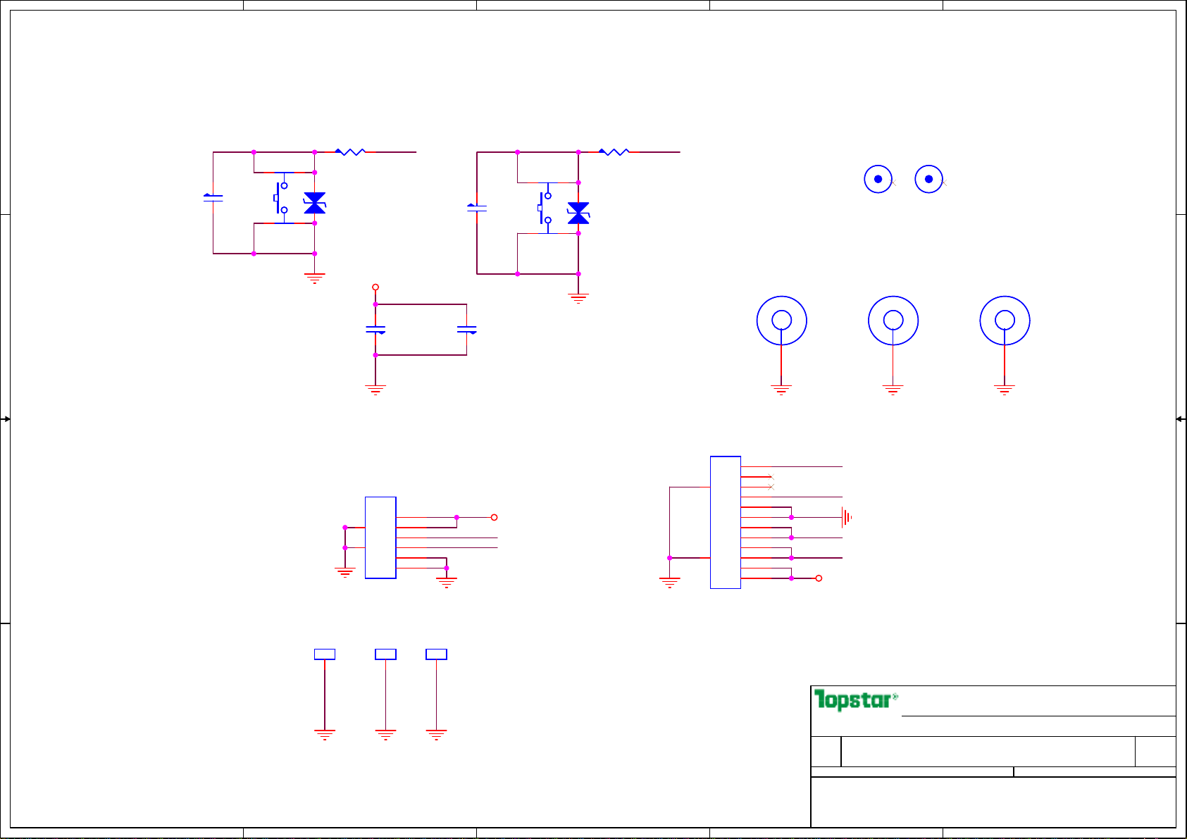
5
4
3
2
1
Touchpad
D D
3
TC1
TC1
100pF/50V,NPO
100pF/50V,NPO
TP
TP
1
L_SW
L_SW
TD-13XA
TD-13XA
BUTTON4_S
BUTTON4_S
TP
TP
C C
TR1
TR1
1K
1K
R0402
R0402
TP
TP
4
12
TESD1
TESD1
ESDPAD_R0603
ESDPAD_R0603
EGA1-0603-V05
EGA1-0603-V05
ns
ns
2
TR2
TR2
1K
1K
R0402
LEFT RIGHT
3
TC2
TC2
100pF/50V,NPO
100pF/50V,NPO
TP
TP
1
R_SW
R_SW
TD-13XA
TD-13XA
BUTTON4_S
TP_+V5S
TC3
TC3
0.1UF/10V,X5R
0.1UF/10V,X5R
C0402
C0402
TP
TP
BUTTON4_S
TP
TP
TC4
TC4
0.1UF/10V,X5R
0.1UF/10V,X5R
C0402
C0402
TP
TP
R0402
TP
TP
4
12
TESD2
TESD2
EGA1-0603-V05
EGA1-0603-V05
ESDPAD_R0603
ESDPAD_R0603
ns
ns
2
TH2
TH2
HOLE
HOLE
1
TH_315_410_230
TH_315_410_230
ns
ns
TFD2
TFD2
1
1
FMARKS
FMARKS
ns
ns
TH1
TH1
1
TH_R217X268_100
TH_R217X268_100
TFD1
TFD1
1
FMARKS
FMARKS
ns
ns
HOLE
HOLE
ns
ns
1
TH3
TH3
HOLE
HOLE
1
TH_R217X268_100
TH_R217X268_100
ns
ns
TP_CAP1
TP_CAP1
12
TP1
TP1
INT_spkR 6Pin
INT_spkR 6Pin
CNS6_0D5_RA1
CNS6_0D5_RA1
6
6
5
8
4
3
7
2
1
TP
TP
TE3
TE3
1
EMI
EMI
1
ns
ns
EMIPOINT
EMIPOINT
5
4
3
2
1
EMIPOINT
EMIPOINT
TE2
TE2
1
EMI
EMI
1
ns
ns
B B
8
7
TE1
TE1
1
EMI
EMI
1
ns
ns
EMIPOINT
EMIPOINT
A A
5
4
TP_TPCLK
TP_TPDAT
TP_+V5S
3
12
11
14
10
14
9
8
7
6
5
4
13
3
13
2
1
TPCON_USB
TPCON_USB
CNS12_0D5_RA1
CNS12_0D5_RA1
TP
TP
11
10
9
8
7
6
5
4
3
2
1
RIGHT
LEFT
TP_TPCLK
TP_TPDAT
TP_+V5S
TOPSTAR TECHNOLOGY
TOPSTAR TECHNOLOGY
TOPSTAR TECHNOLOGY
Swain Xu(
Swain Xu(
Swain Xu(
)
)
Touchpad Board
Touchpad Board
Page Name
Page Name
Page Name
Size
Size
Size
Project Name Rev
Project Name Rev
Project Name Rev
A4
A4
A4
Date: Sheet
Date: Sheet
Date: Sheet
PROPERTY NOTE: this document contains information confidential and property to
PROPERTY NOTE: this document contains information confidential and property to
PROPERTY NOTE: this document contains information confidential and property to
TOPSTAR and shall not be reproduced or transferred to other documents or disclosed
TOPSTAR and shall not be reproduced or transferred to other documents or disclosed
TOPSTAR and shall not be reproduced or transferred to other documents or disclosed
to others or used for any purpose other than that for which it was obtained without
to others or used for any purpose other than that for which it was obtained without
to others or used for any purpose other than that for which it was obtained without
the expressed written consent of TOPSTAR
the expressed written consent of TOPSTAR
the expressed written consent of TOPSTAR
2
Touchpad Board
P01
P01
P01
)
39 39Friday, April 30, 2010
39 39Friday, April 30, 2010
39 39Friday, April 30, 2010
of
of
of
1
A
A
A
 Loading...