

Page 1

第 1 页,共 122 页
维 修 手 册
型号:
LCD26P08/LCD26P08A
LCD32P08/LCD32P08A
LCD37P08/LCD40P08
LCD42P08/LCD42P08A
P08系列 中文维修手册仅用于维修参考
Page 2

目录
第 2 页,共 122 页
封面------------------------------------------------------------------------------------1
目录------------------------------------------------------------------------------------2
1 安全与注意事项--------------------------------------------------------------------------4
1.1 安全注意事项----------------------------------------------------------------------4
1.2 操作使用注意点--------------------------------------------------------------------4
1.3 高压警告--------------------------------------------------------------------------4
1.4 静电敏感器件(ESD)注意事项-------------------------------------------------------4
1.5 安装注意事项----------------------------------------------------------------------4
2 液晶电视规格----------------------------------------------------------------------------6
2.1 基本规格---------------------------------------------------------------------------6
2.2 LCD TV 描述------------------------------------------------------------------------7
2.3 电源连接---------------------------------------------------------------------------7
3 操作说明及调整--------------------------------------------------------------------------8
3.1 遥控器说明------------------------------------------------------------------------8
3.2 正面示意图及控制面板--------------------------------------------------------------9
3.3 菜单功能-------------------------------------------------------------------------10
4 连接介绍-------------------------------------------------------------------------------13
4.1 底面及背面连接示意图--------------------------------------------------------------13
4.2 后AV连接示意图--------------------------------------------------------------------13
4.3 机内连接示意图--------------------------------------------------------------------13
1. LCD26P08A---------------------------------------------------------------------14
2. LCD32P08A---------------------------------------------------------------------15
3. LCD37P08----------------------------------------------------------------------16
4. LCD42P08A---------------------------------------------------------------------17
5 TV电气方框图---------------------------------------------------------------------------18
6 故障处理流程------------------------------------------------------7 PCB LAYOUT ----------------------------------------------------------------------------24
7.1 主板-----------------------------------------------------------------------------24
7.2 电源板---------------------------------------------------------------------------26
1. MIP260B-19(LCD26P08A)---------------------------------------------------------26
2. MIP320G-A(LCD32P08A)----------------------------------------------------------27
3. MIP328B-K-1(LCD37P08)---------------------------------------------------------29
4. MIP988-J(LCD42P08A)-----------------------------------------------------------31
7.3 IR 板----------------------------------------------------------------------------34
7.4 SIED AV板------------------------------------------------------------------------34
7.5 按键转接板与薄膜按键-------------------------------------------------------------35
8 电路图---------------------------------------------------------------------------------36
8.1 主板-----------------------------------------------------------------------------36
8.2 电源板---------------------------------------------------------------------------43
1. MIP260B-19(LCD26P08A)---------------------------------------------------------43
2. MIP320G-A(LCD32P08A)----------------------------------------------------------48
3. MIP328B-K-1(LCD37P08)---------------------------------------------------------52
4. MIP988-J(LCD42P08A)-----------------------------------------------------------56
9.3 IR 板----------------------------------------------------------------------------60
8.4 按键板---------------------------------------------------------------------------61
9 主要芯片规格-------------------------------------------------------------------------62
9.1 TSUMV36K--------------------------------------------------------------------------63
--------------------19
Page 3

9.2 AT24CXX---------------------------------------------------------------------------70
第 3 页,共 122 页
9.3 AT26DF081A------------------------------------------------------------------------73
9.4 TDA7266SA-------------------------------------------------------------------------77
9.5 LD1117----------------------------------------------------------------------------79
10 屏&电源接口说明-----------------------------------------------------------------------86
10.1 屏接口说明-----------------------------------------------------------------------86
1.IVO M260TWR1 R1-----------------------------------------------------------------86
2.LG LC320WXE SB V1---------------------------------------------------------------91
3.LG LC370WXE SV V2---------------------------------------------------------------95
4.AUO T420HW06 V.3----------------------------------------------------------------99
10.2 电源接口规格--------------------------------------------------------------------103
1.MIP260B-19---------------------------------------------------------------------103
2. MIP320G-A---------------------------------------------------------------------105
3. MIP328B-K-1-------------------------------------------------------------------107
4. MIP988-J----------------------------------------------------------------------110
11 爆炸图-------------------------------------------------------------------------------111
12 软件升级-----------------------------------------------------------------------------115
Page 4

1. 安全与注意事项
第 4 页,共 122 页
1.1 安全注意事项
(1) 为了持续保持安全,不要企图修改电路板。
(2) 在维修之前,断开交流电源。
(3) 维修技术人员配有任何时候都可以使用的准确电压表,这一点至关重要。定期检查电压表的校准。
(4) 请不要使显示器受强烈的外力震动。
1.2 操作使用注意点
(1) 移动显示器之前请拔掉电源接线。
(2) 为安全起见,一些部件被抬高,高过印刷电路板。有时,使用绝缘管或胶带。有时,内部接线被
加起来,目的是为了防止与致热部件接触。把所有此类元件重新安装到其原来的位置
(3) 在维修后,要检查螺钉和接线是否正确地重新安装。要保证维修过的部件周围区域没有损坏。
(4) 请注意在长时间显示同一个画面后关机原来的图象信息可能还保持在上面。
(5) 检查交流插头的插片和易碰到的导电部件(如金属盘、输入端子和耳机塞孔)之间的绝缘情况。
1.3 高压警告
显示器高压是由电源升压板产生的,如果不注意接触到高压,可能被严重电击。
1.4 静电敏感器件(ESD)注意事项
一些半导体(固态)设备很容易被静电损坏,此类部件一般称为静电敏感器件器件(ESD)。典型的
ESD器件有集成电路和一些场效应晶体管。下列方法会减少静电造成部件损坏时间的发生率。
1. 在处理任何半导体部件或组件之前,要立即通过接触已知的接地点,将静电从身体上放到。另一
种发放是,带上放电的腕带装置。为了避免点击的危险,在给液晶电视加电之前,务必取下腕带。
2.在拆除有ESD的组件后,将其放到导电平面(如铝箔)以防积聚静电。
3. 不要使用带氟利昂的化学品,这会产生足以破坏ESD的电荷。
4.仅使用接地的铝铁焊接或焊开ESD.
5. 仅使用防静电除焊装置。一些不属于“防静电”类的除焊装置可能产生以破坏ESD的电荷。
6.在准备安装之前,不要将设备用ESD由保护包装中取出。绝大多数用ESD包装有导线,这些导线通
过导电泡沫与、铝箔或其它导电材料短接。
7. 即将由设备ESD导线上出去保护材料之前,应使保护材料与安装器件的地板和电路组件接触。
注意:不要给底板或电路加电并遵守其它安全注意事项。
8. 在处理没有包装的备用ESD时,要尽量减少身体的运动。一些运动如摩擦衣服或由铺地毯的地板上
抬起脚都会产生足以破坏ESD的静电。
1.5 安装注意事项
1. 为了保障安全,搬运产品需要两人以上。
Page 5

2. 让电源线远离散热设备,否则外壳融化可能导致起火或触电。
第 5 页,共 122 页
3. 不要将产品置于通风不良的区域,如书架和壁橱。内部温度升高可能造成起火。
4. 把外部天线接到产片上时,要弯曲内部天线。该措施旨在防止天线受潮。否则,可能造成
起火或触电。
5. 必须保证在重新放置产品之前关闭电源并从插座拔下电源线。如果天线或外部链接器未完
全插入,还应检查天线或外部连接器。天线损坏可能造成起火或触电。
6. 让天线远离高压线,并将天线安装牢靠。与高压线接触或天线掉下来可能造成起火或触电。
7. 当安装产品时,在产品和墙壁之间留下足够的空间(10cm),以便通风。
Page 6
2. 液晶电视规格
第 6 页,共 122 页
2.1 基本规格
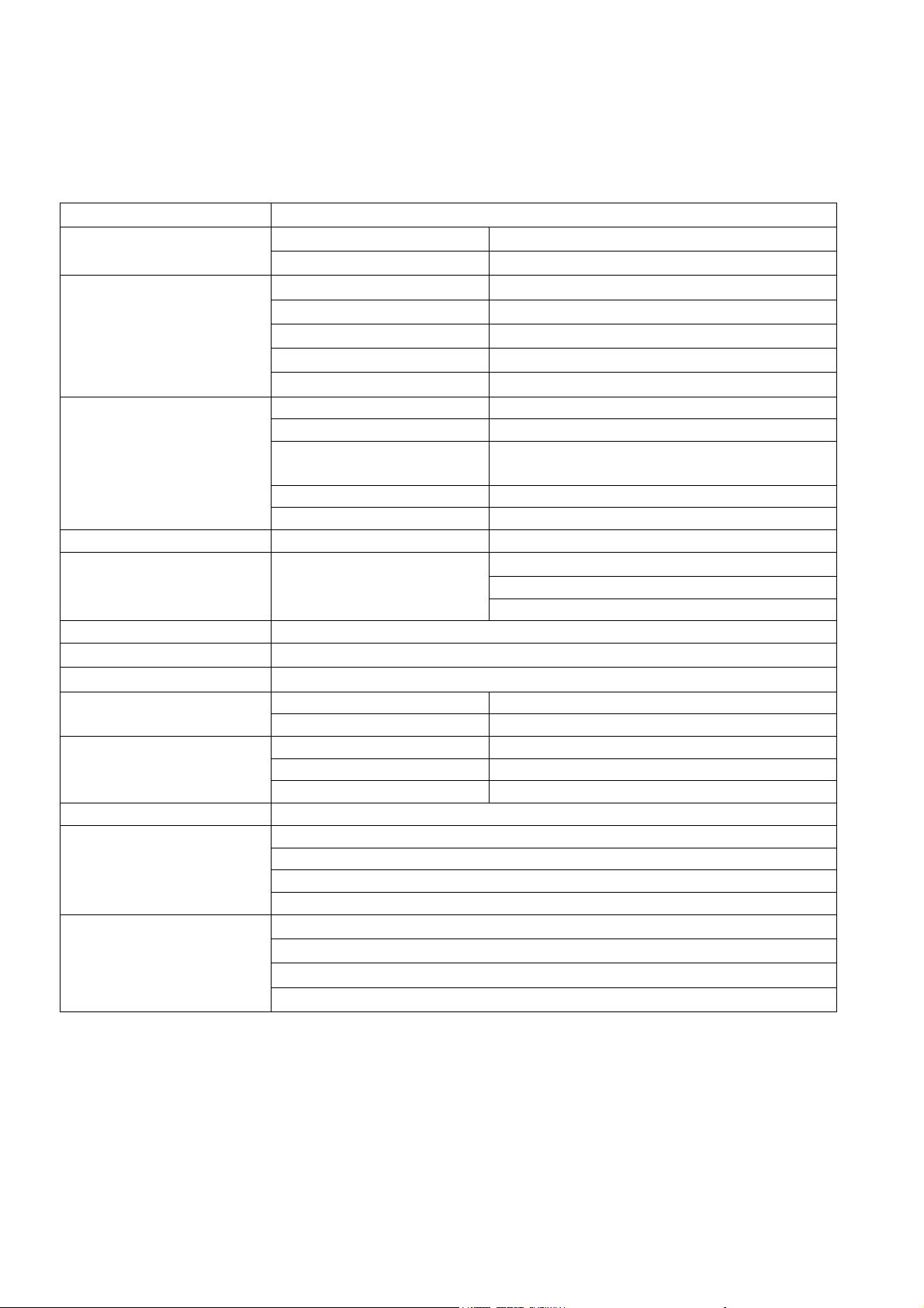
项目 液晶电视
电视功能
视频输入
PC 输入
视频输出功能 输出TV/AV1/AV2/ 视频输出(RCA)
音频输出 音频输出音频输出:L/R
OSD 语言 中文/英文(出厂设定为中文)
底座
墙壁装配件
电源
使用环境
附件 遥控器、电池(AAAX2)、电源线、保修单、使用说明书
电脑支持的格式
高清支持的模式
电视标准 PAL B/G、D/K、I
声音系统
FM-MONO
视频1 RCA x 2(音频L/R x 2)
视频2 RCA x 2(音频L/R x 2)
S端子 x 1
高清信号 Y、Pb、Pr x 1
影音端子 HDMI x 1
信号输入 模拟:D-Sub 15 针
即插即用兼容 DDC
输入频率
推荐 模拟:1360x768 (60Hz)
音频输入 用于立体声的耳机迷你型插孔(3.5 ø)
模拟:FH:31.5kHz 到 50kHz
FV:60Hz 到75Hz
扬声器(内置):6Wx2(L/R)
用于立体声的耳机迷你型插孔(3.5 ø)
声音输出(RCA L/R)
可选
可选
电源 AC 100V~240V, 50/60HZ
功率消耗 26”:120W/32”:140W/37”:200W/42”:240W
温度 + 0 °C ~ + 40 °C
储存温度 - 25 °C ~ + 60 °C
湿度 10% ~ 85%
640 x 480 (60/75Hz)
800 x 600 (60/75Hz)
1024 x 768 (60Hz)
1360x768(60Hz)
480i/p
576i/p
720p
1080i/p
Page 7

2.2 LCD TV 描述
第 7 页,共 122 页
该 LCD TV 包含主板(内置音频板)、开关电源板(含逆变器)、遥控接收板、按键板。主板和电源
板含 I
给液晶模块去驱动LCD显示电路。
2C 逻辑控制总线, DDC, LCD panel 的亮度逻辑控制和通过DC-DC 转换器来提供整个主板和TTL信号
2.3 电源连接
将电源线一端插入本机后下方的“交流输入”插孔内,另一端接入市电220V的电源插座上。
在您未切断电源而处于待机的情况下,电视机始终会消耗部份功率。
在长时间不使用电视情况下 , 最好将下面的电源开关关闭并将电源线从电源插座中拔下。
Page 8
3 操作说明及调整
第 8 页,共 122 页
3.1 遥控器说明
电源
按这个键可以打开或待机,但电视不会完全断
电,处于节能状态。
信源
按此键可显示当前可选信源,按
0-9
用来选择电视频道。
显示
(1)当使用电视信号时显示频道号码及声音模
式。
(2)当使用电视信号之外的其它输入时,显示当前
输入源等信息
、 选择
-
回看
用来显示前一次选择的电视频道。
音量+、-键
在进入菜单状态时可以用作确认和参数调整;在未
进入菜单时为音量的加减。
频道+、-键 、
在进入菜单时进行上下选择在未进入菜单时
静音
中断声音或恢复声音。
菜单
菜单下是返回主菜单,在信源下是确认功能
图像大小
包含2 种模式,重复按可切换为满屏/标准。
方向键 、 、 、
在菜单中选择各个子菜单
声音模式
可选择关、立体声、新闻、电影、音乐、环绕
音与自设定。
彩色模式
调整成标准色温,暖色温与冷色温
睡眠
使用这个按键,您可以设置电视在多长时间之
后进入待机状态。重复按这个键可以在 关闭、
15、30、45、60、90 和120 分钟之间选择。(定
时器从菜单消失之后所选择的分钟开始倒数计
时。
图像制式
可以快捷更改TV制式。
图像静止
打开与关闭画面静止
丽音
选择丽音通道
Page 9
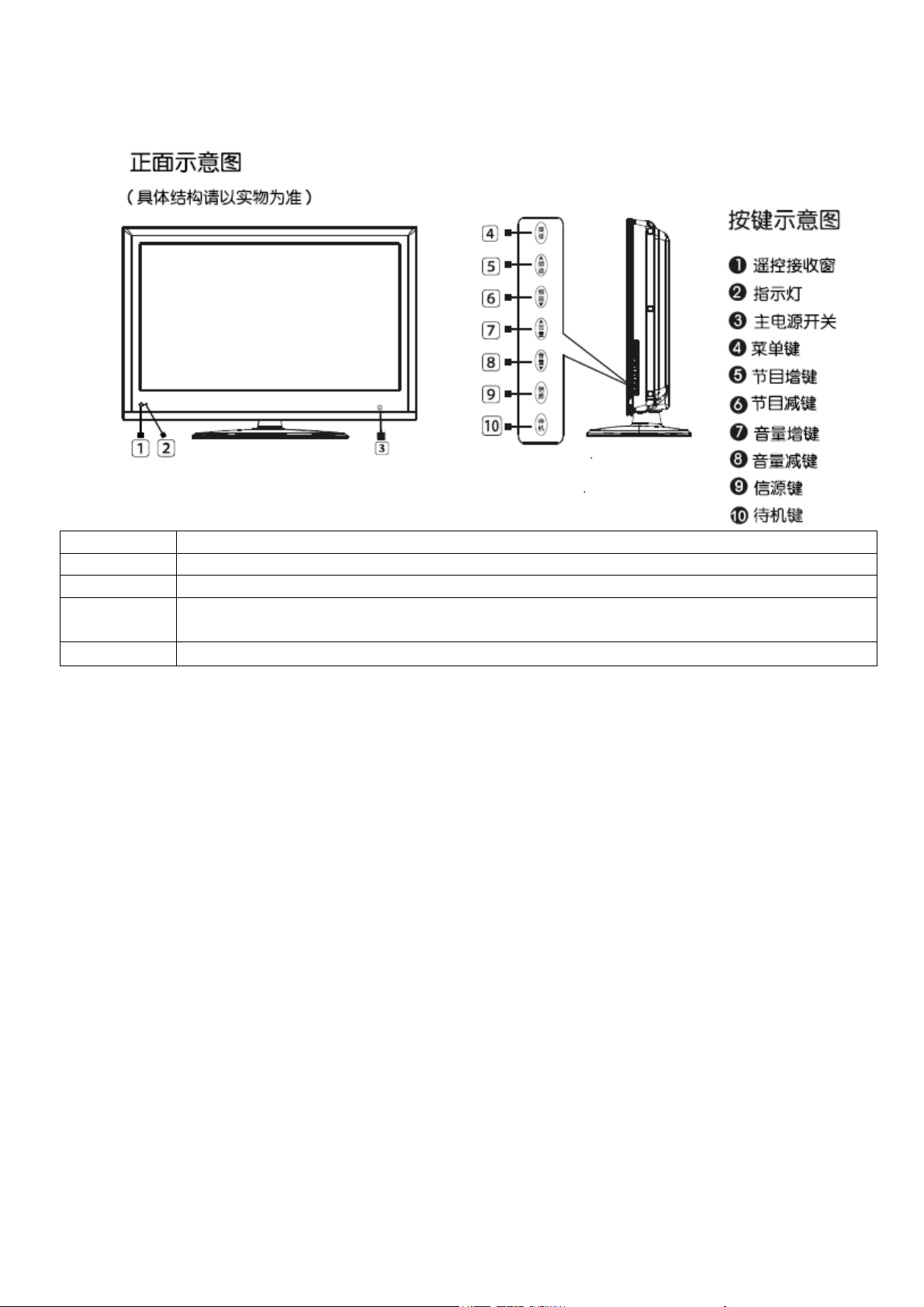
3.2 正面示意及控制面板
第 9 页,共 122 页
待机键: 按此键可以打开或使电视进入待机状态,如果电视处在待机状态,则前面的指示灯会亮起红色。
信源键: 按此键可以变换不同的输入信源。
菜单: 按此键可以进入或退出菜单。
节目增减键:
音量增减键:
在屏幕出现菜单时,按此两键可以选择所要执行选项,在屏幕无OSD 菜单时,为TV模式时可以
换台。
在屏幕出现菜单时,按此两键可以确认所选择之选项,在屏幕无OSD 菜单时,为音量之调整。
Page 10

3.3 菜单功能
第 10 页,共 122 页
使用菜单
1.按菜单按钮可以显示或关闭菜单菜单。
2.使用左或右键可以选择所要调整之菜单选项。
3.使用上或下键可以进入子菜单表,或启用或调整所选择之功能,光标所在位置为调整状态。
4.按菜单按钮可以退出菜单。
电视/视频信源下的菜单画面
(注意:在不同的信源下,所能调节的功能有所不同)
按菜单按钮进入主菜单,调节项目包括:图像、声音、系统、高级、电视、电脑。请见以下详述:
图像
1. 图像模式-选择合适的图像效果(注:四种状态可选,分别是标准、艳丽、柔和、用户)。
2. 对比度-调节画面黑白层次,适当的对比度可使画面清晰明亮。
3. 亮度-调节画面的背景亮度,一般与对比度配合使用。
4. 色调-调节色彩的色调(注:只在NTSC制式图像状态下才可以选择和调整功能)。
5. 饱和度-调节色彩的鲜艳度、饱和度(注:电脑状态下无此选项)。
6. 清晰度-调节画面清晰度(注:电脑状态下无此选项)。
7. 色温-调节画面的冷暖感觉(注:三种状态可选,分别是标准、暖色、冷色)。
8. 图像大小-选择合适的图像模式(注:两种状态可选,分别是满屏和标准)。
Page 11

声音
第 11 页,共 122 页
1. 声音模式-调节声音模式(注:四种状态可选,分别是用户、标准、新闻、音乐)。
2. 低音-调节电视机的声音低频效果。
3. 高音-调节电视机的声音高音效果。
4. 平衡-调节左右音箱大小比例、
系统
1. 菜单语言-选择语言的种类(注:两种语言可选,分别是中文、英文)。
2. 菜单透明度-选择调节OSD的透明亮度。
3. 复位-初始化设置。
高级
1. 图像降噪-图像噪点抑制(注:有四种状态可选,分别是关、低、中、高)
2. 睡眠时间-设定睡眠关机时间(注:有七种状态可选,分别是关、15、30、45、60、90、120)
Page 12

电视
第 12 页,共 122 页
1. 频道-选择频道。
2. 彩色制式-选择视频信号制式(有三种状态可选,分别是自动、PAL、SECAM)。
3. 声音制式-选择伴音信号制式(有四种状态可选,分别是D/K、M、B/G、I)。
4. 跳跃-台号跳跃功能。
5. 微调-微调功能
6. 手动搜台-手动搜台功能。
7. 自动搜台-自动搜台功能。
8. 丽音-选择丽音或者单声道(注:当地电视台如有发送丽音伴音信号,才能选择。)
电脑(只在电脑信源下有作用)
1. 水平位置-调节画面的水平位置。
2. 垂直位置-调节画面的垂直位置。
3. 时钟-调节画面的时钟频率。
4. 相位-调整A/D的采样相位。
5. 自动-自动调节屏幕显示到最佳状态
Page 13

4.连接介绍
第 13 页,共 122 页
4.1 底面及背面连接示意图
4.2 后AV端子示意图
Page 14
4.3 机内连接示意图
第 14 页,共 122 页
1、LCD26P08A
二合一电源板
二合一电源板
T-CON 板
LCD 显示屏
薄膜按键
按键转接板
喇叭
主板
主板
侧 AV 板
SIDE AV 板
接收板
接收板
Page 15
2.LCD32P08A
第 15 页,共 122 页
二合一电源板
T-CON 板
LCD 显示屏
薄膜按键
按键转接板
主板
SIDE AV 板
接收板
喇叭
Page 16
3.LCD37P08
第 16 页,共 122 页
电源板 T-CON 板 LCD 显示屏
逆变器(左)
薄膜按键
按键转接板
逆变器(右)
主板
SIDE AV 板
接收板
喇叭
Page 17
第 17 页,共 122 页
平衡板
逆变器
3.LCD42P08A
电源板 T-CON 板 LCD 显示屏
薄膜按键
按键转接板
主板
SIDE AV 板
接收板
喇叭
Page 18

5. TV电气方框图
第 18 页,共 122 页
Page 19
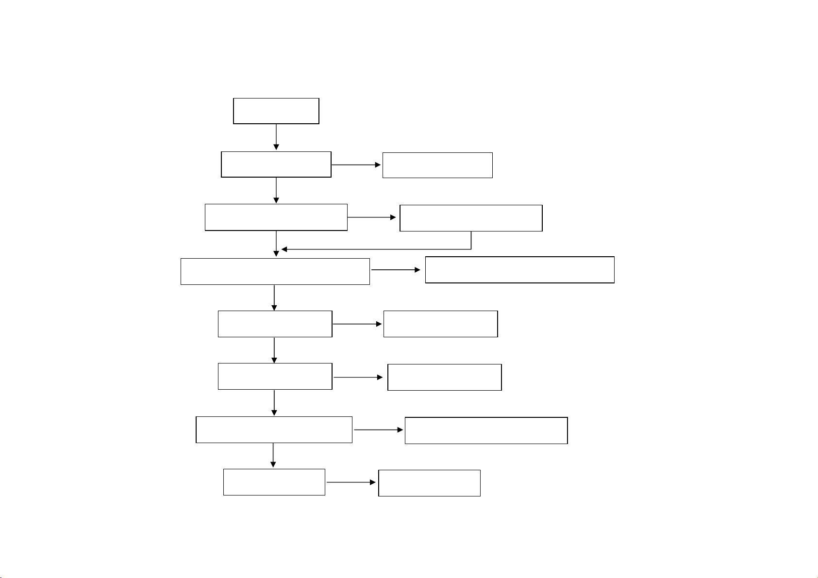
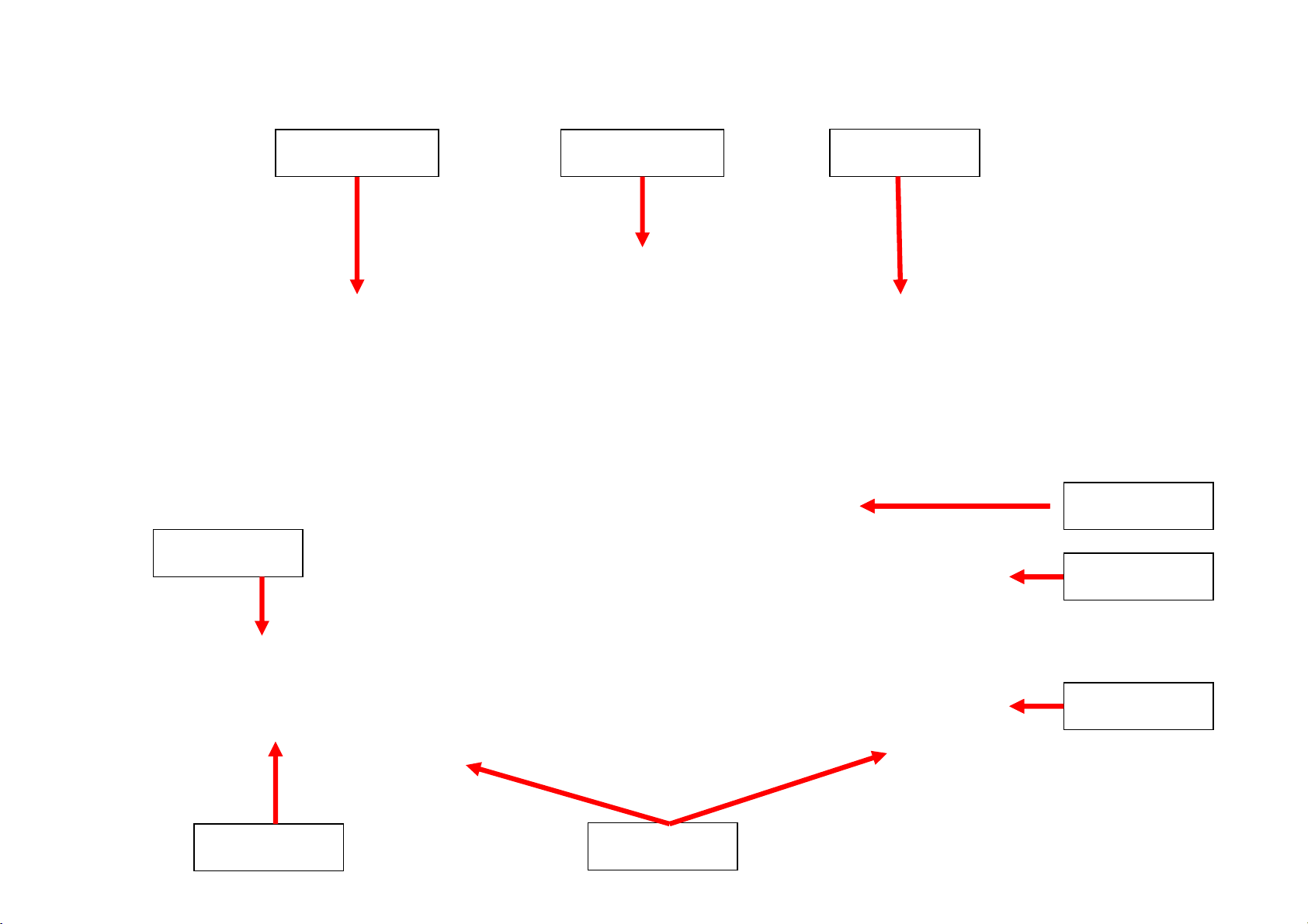
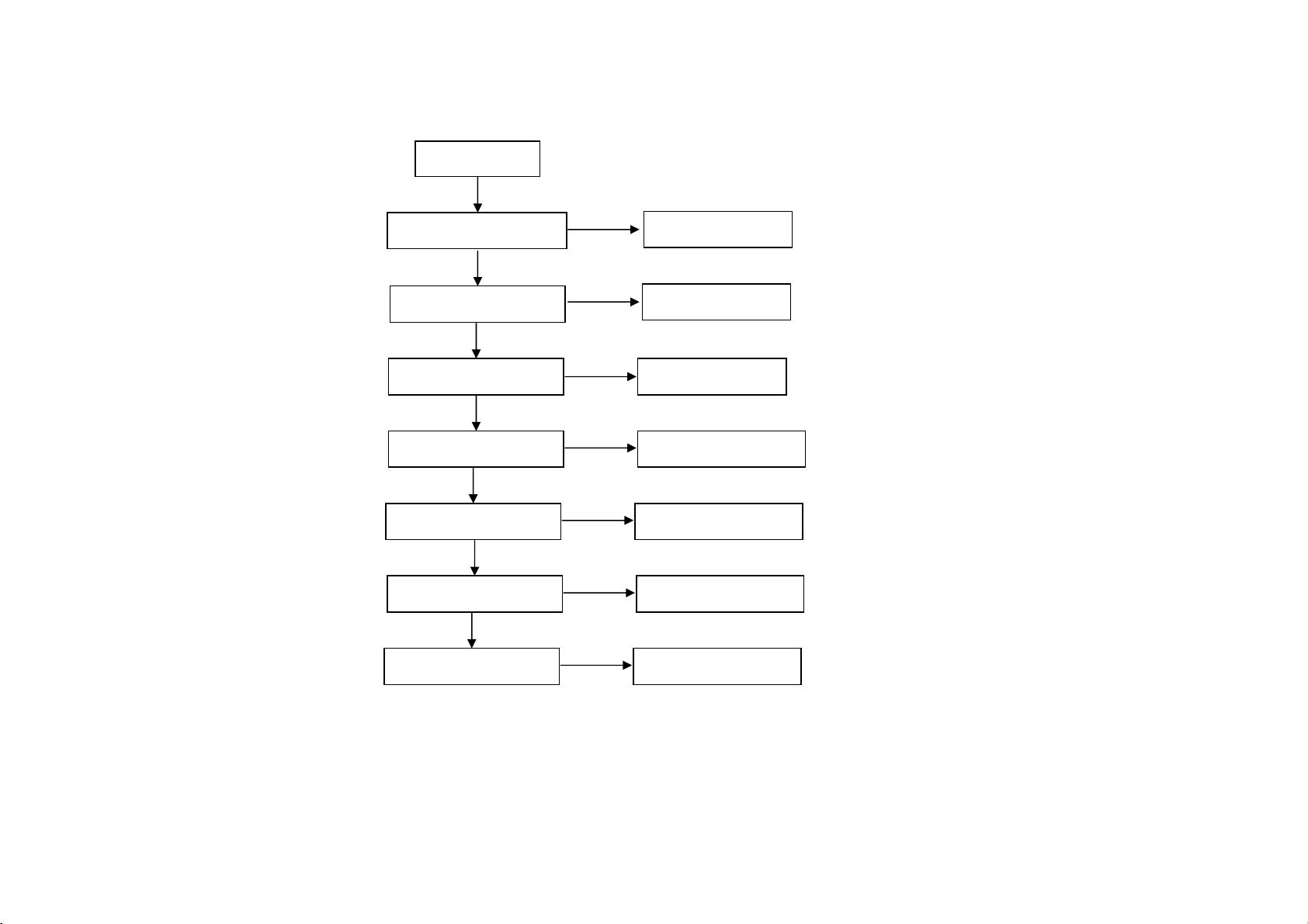
6.故障处理流程
K
第 19 页,共 122 页
6.1板故障处理
1、 无显示(LED不亮)
检查U2、Q104、D109(VCC)
不加电
检查电源接口
OK
检查F1、BD1、D101
O
OK
OK
检查 T103
OK
检查 D103、D13、Z101
OK
检查 L404
NG
重插接口
NG
更换F1或BD1或D101
检查负载
NG
更换U2或Q104或D109
NG
更换 U1 或 Q101 检查 U1、Q101
NG
更换 T103
NG
更换 D103 或 D13 或 Z101
NG
检查 L404
Page 20
2、 无显示(LED亮红色灯)
红色
K
K
K
K
K
K
第 20 页,共 122 页
无显示
LED
检查 +3.3V_STB
O
检查 +3.3V
O
检查 VCC1.26V
O
检查 Q15、D43
O
检查 X1
O
检查 U14
O
检查 U15
NG
NG
NG
NG
NG
NG
NG
更换 U4
更换 U3
更换 U1
更换 Q15、D43
更换 X1
更换 U14
更换 U15
Page 21
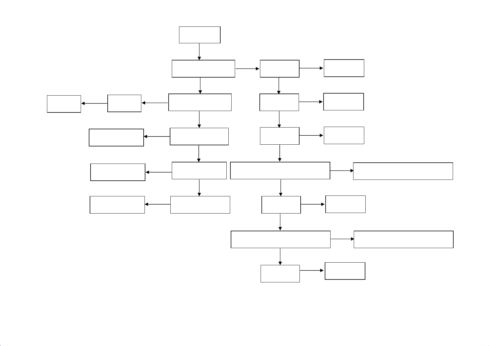
3、 无显示(LED不亮)
第 21 页,共 122 页
更换Q8
NG
更换 Q20 或 Q19
检查Q8
更换 U17
更换 U15 程序
NG
NG
NG
NG
无显示
检查主板 12V 供电
OK
检查主板 5V 供电
OK
检查 CN503 3、4
OK
检查 LVDS VCC
OK
检查 LVDS sigal
NG
检查 Z102
NG
更换 Z102
OK
NG
检查 L105
更换 L105
OK
NG
检查 L105
更换 L105
OK
NG
检查 D104、D105、D106、D107
更换 D104 或 D105 或 D106 或 D107
OK
NG
检查 T101
更换 T101
OK
NG
检查 T102、Q102、Q103 更胡 T102 或 Q102 或 Q103
OK
NG
检查 U102
更换 U102
Page 22
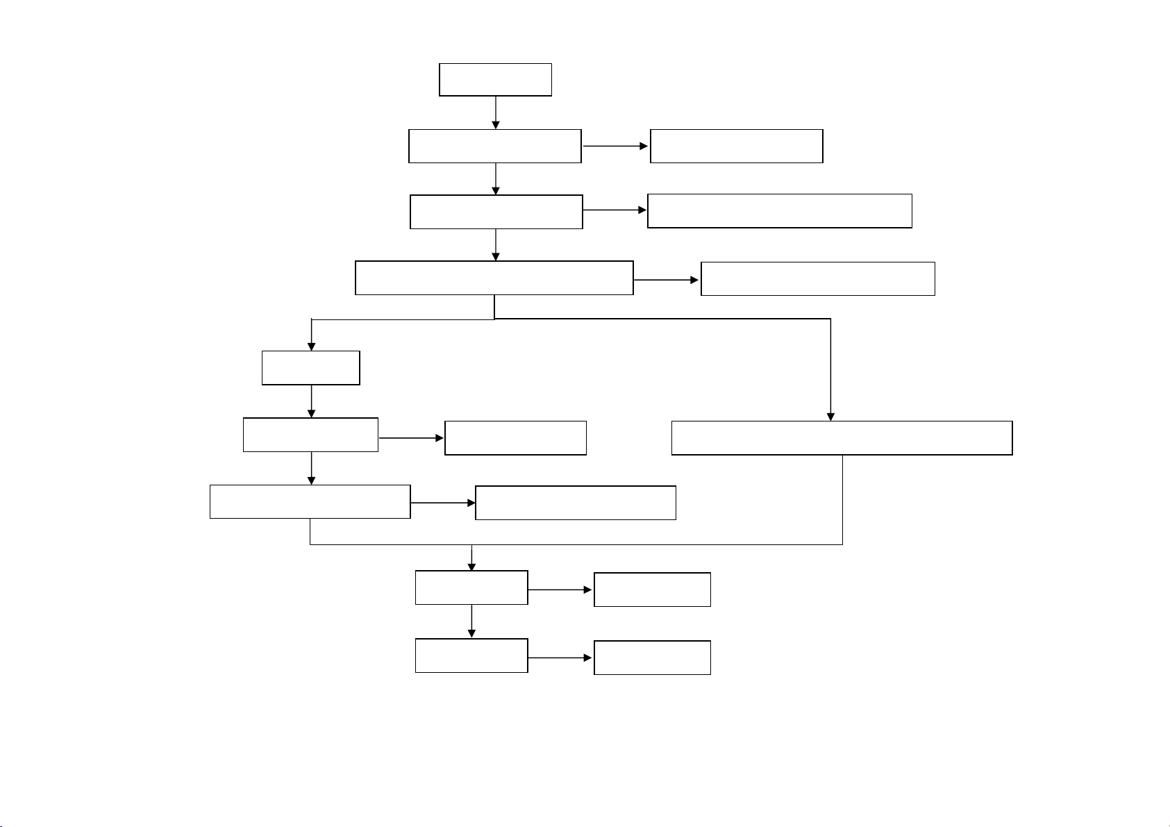
4、 画面异常
K
K
K
K
K
第 22 页,共 122 页
TV 信号
TV 信号制式
O
检查高频头、声表面
画面异常
检查信号源 更换信号源
O
检查 LVDS 线连接
O
检查各输入端滤波电容和磁珠
NG
重设信号制式
NG
更换高频头、声表面
O
检查 U8
NG
O
检查 PANEL
NG
NG
NG
重插 LVDS 接口或更换 LVDS 线
NG
更换 U8
更换 PANEL
更换入端滤波电容和磁珠
AV、S-VIDEO、YPbPr、VGA、HDMI 信号
Page 23
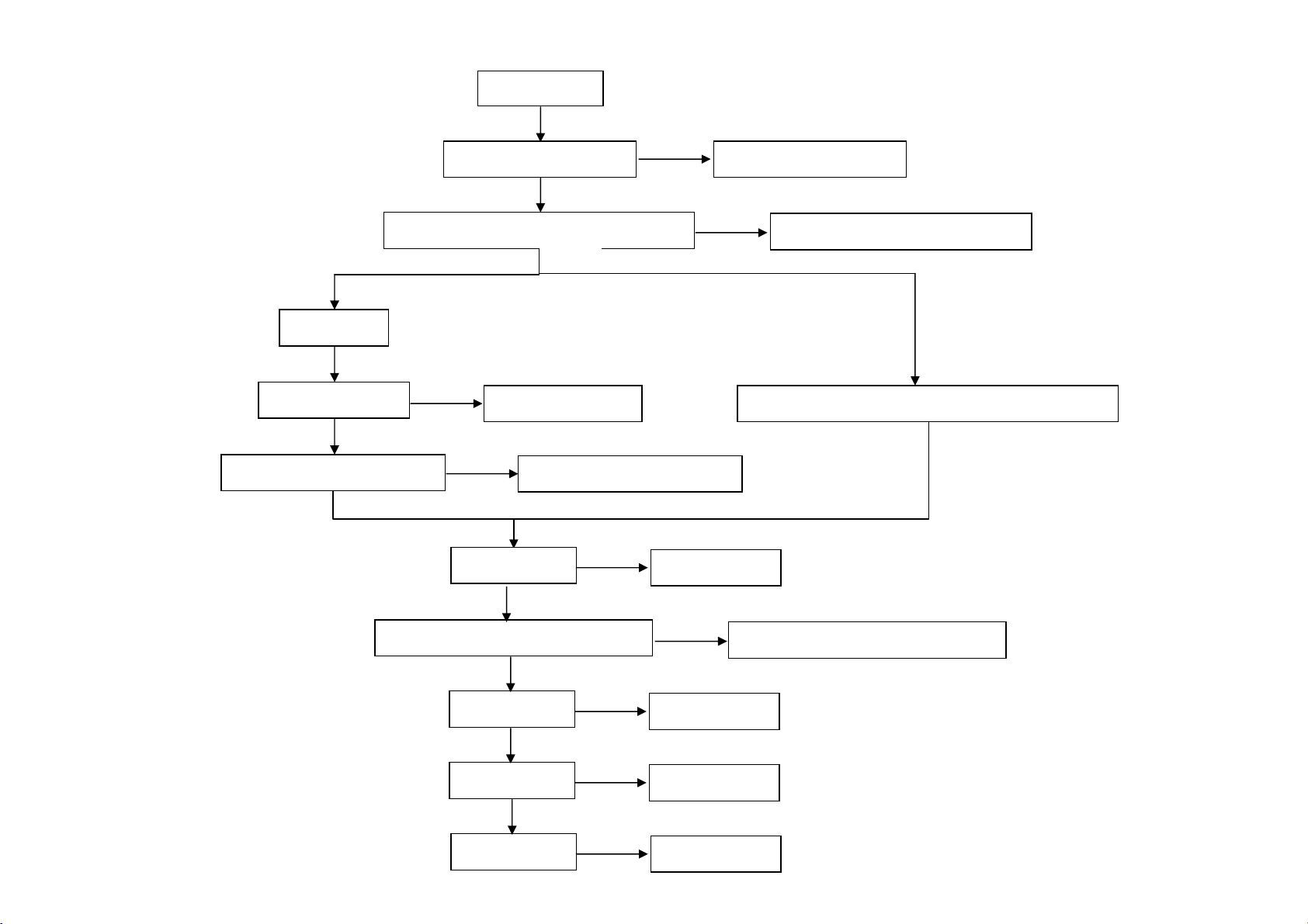
5、 无声
K
K
K
K
K
K
第 23 页,共 122 页
TV 信号
TV 信号制式
OK
检查高频头、声表面
检查 Q40、Q26、Q39、Q23
无声
检查信号源 重插信号源
O
检查各输入端滤波电容和磁珠
O
NG
重设信号制式
NG
更换高频头、声表面
O
检查 U8
NG
O
检查 Q12
NG
O
检查 U12
NG
O
检查喇叭
NG
NG
NG
更换 U8
NG
更换 Q12
更换 U12
更换喇叭
更换入端滤波电容和磁珠
AV、S-VIDEO、YPbPr、VGA、HDMI 信号
更换 Q40 或 Q26 或 Q39 或 Q23
Page 24
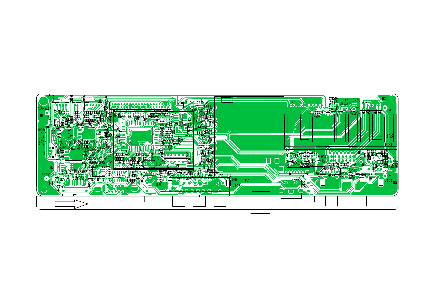
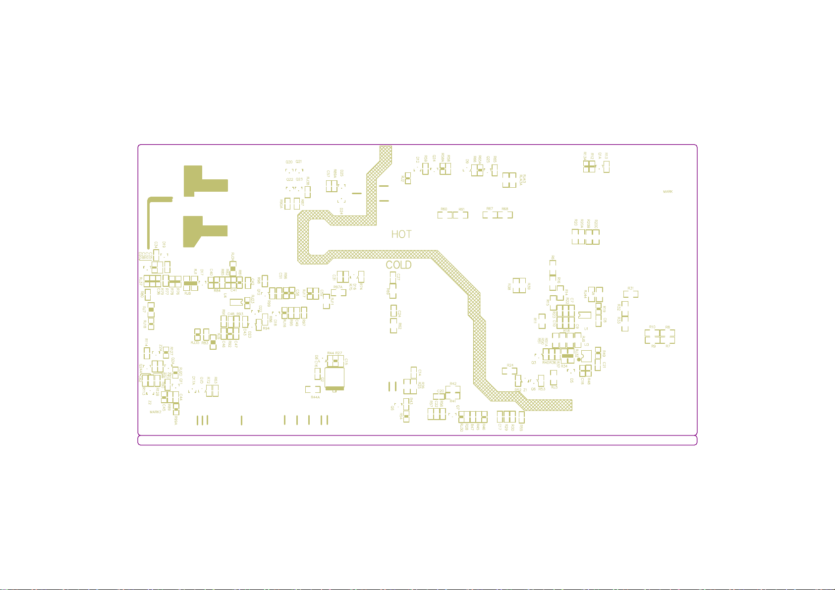
5 PCB LAYOUT
5.1 主板
正面视图
第 24 页,共 122 页
Page 25
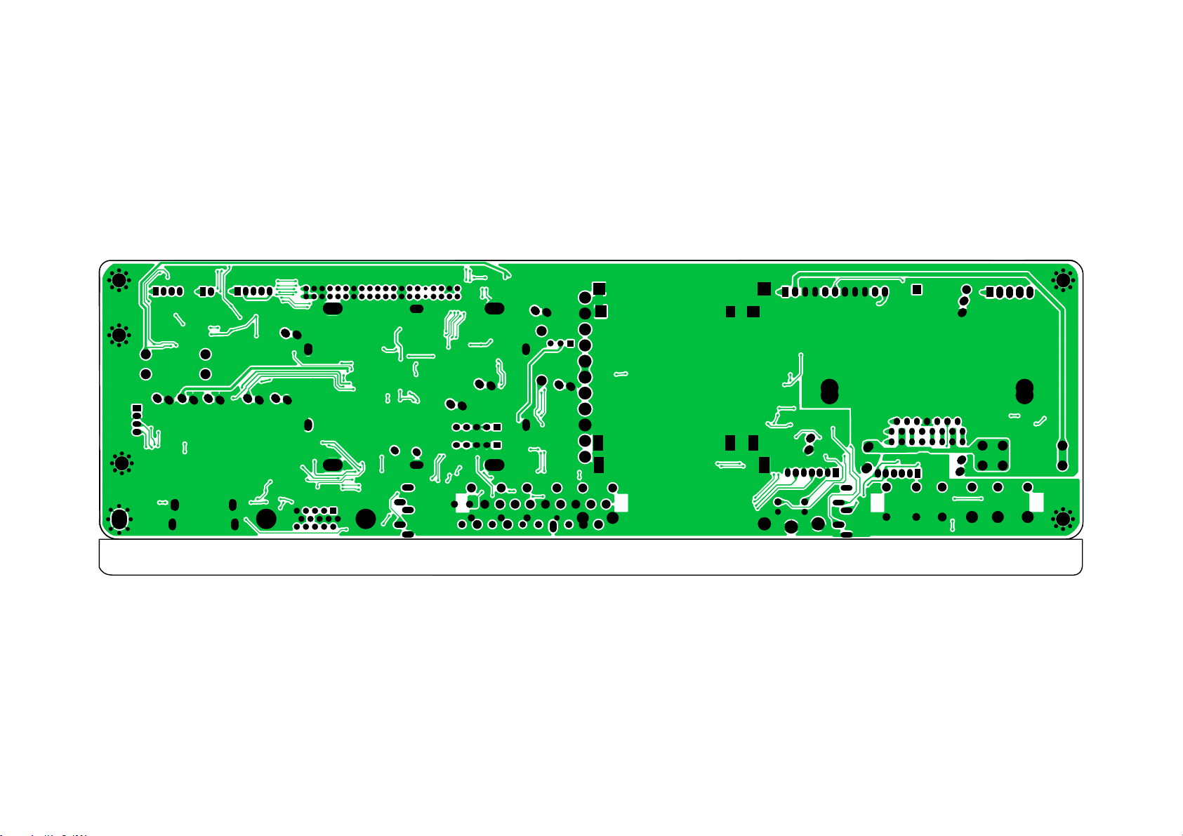
第 25 页,共 122 页
Page 26
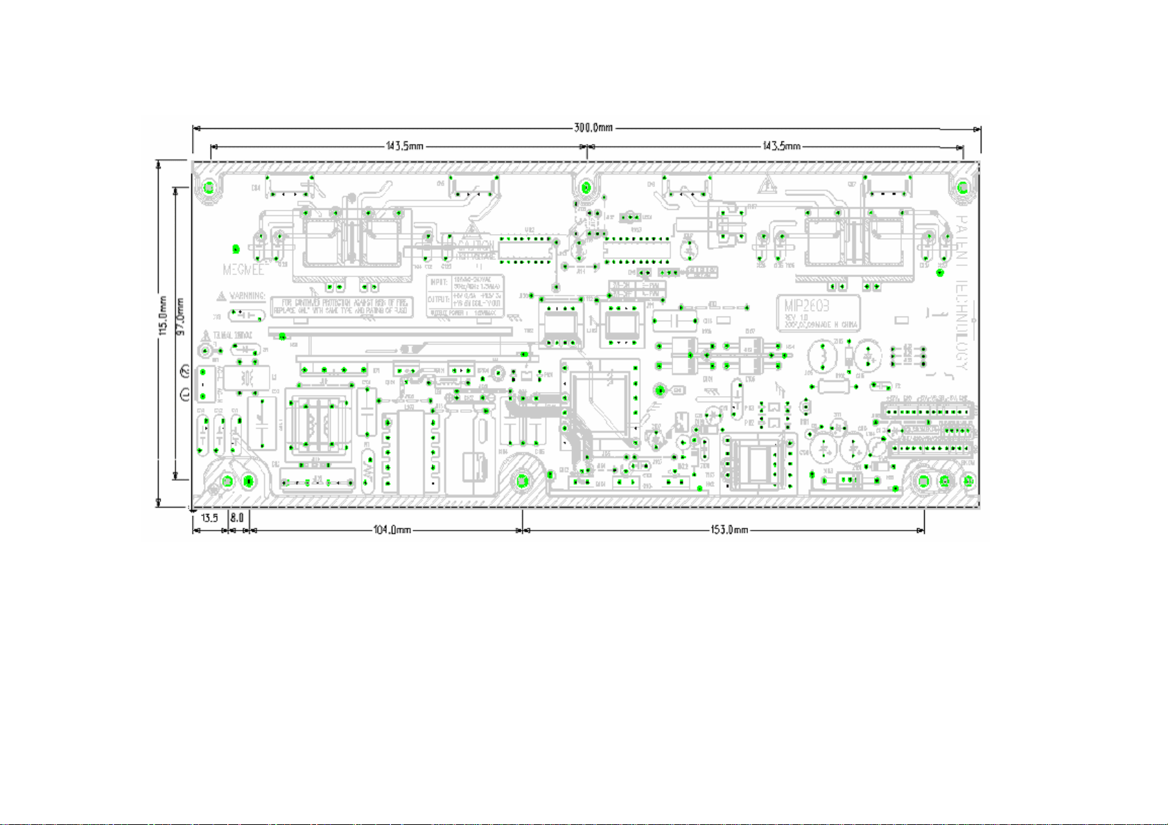
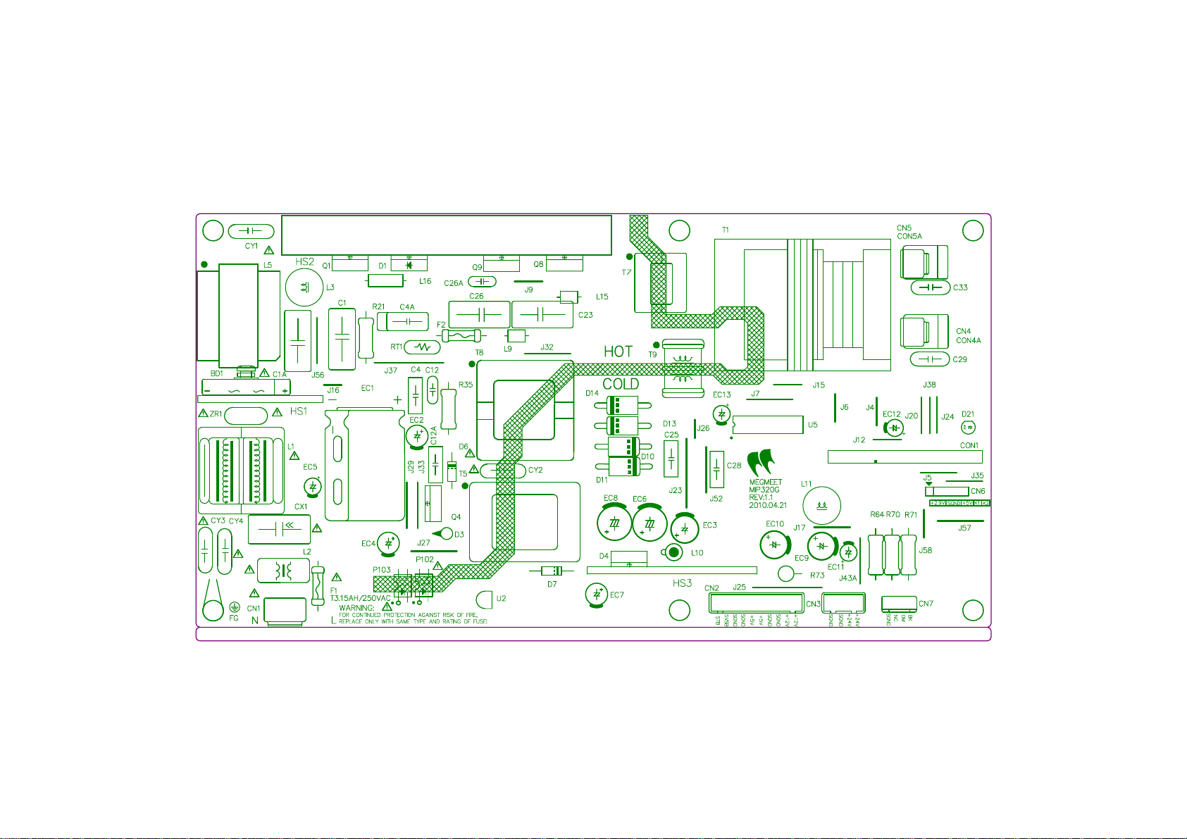
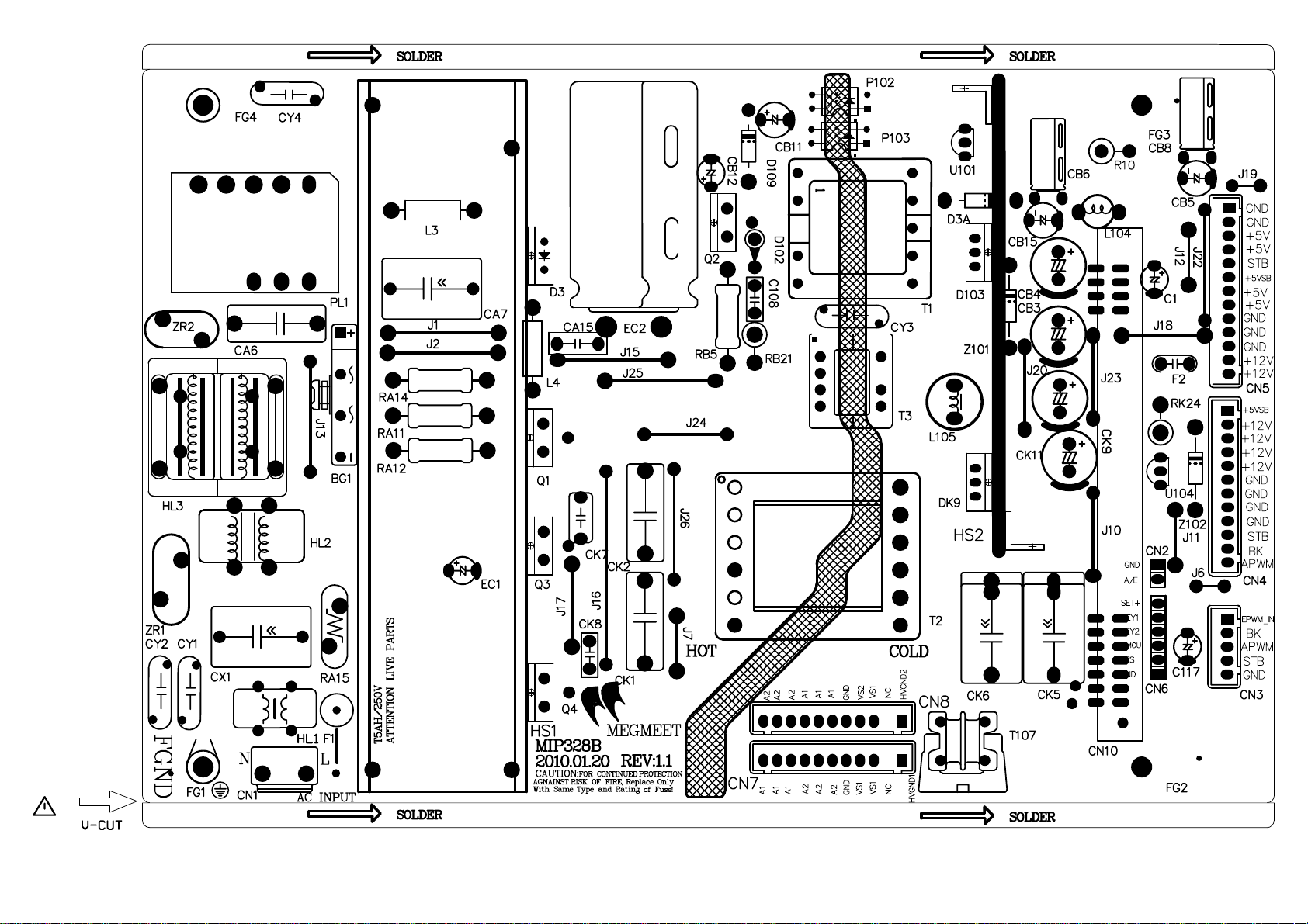
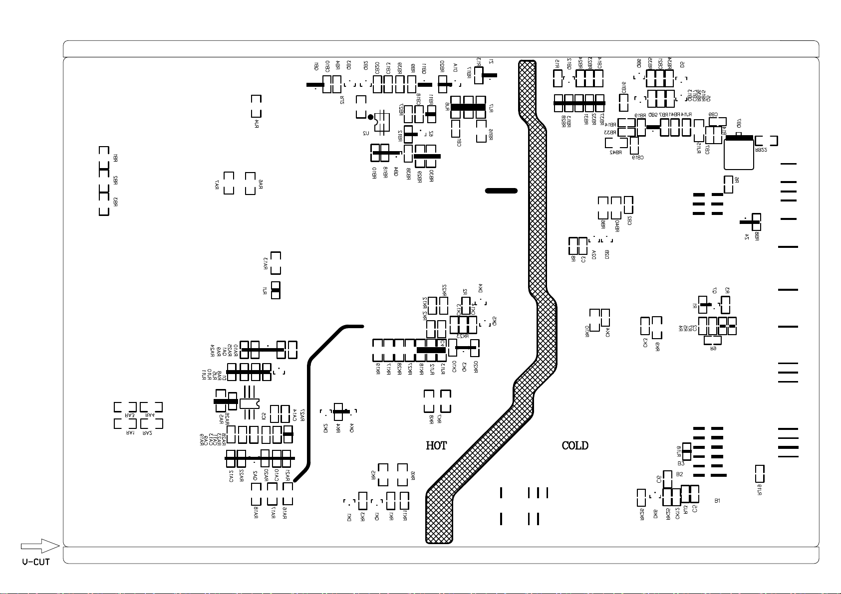
5.2 电源板
第 26 页,共 122 页
1.MIP260B-19(LCD26P08A)
Page 27
2、MIP320G-A(LCD32P08A)
1) TOP
第 27 页,共 122 页
Page 28
2)BOTTOM
第 28 页,共 122 页
Page 29
3、MIP328B-K-1(LCD37P08)
1)TOP
第 29 页,共 122 页
Page 30
2)BOTTOM
第 30 页,共 122 页
Page 31

4、MIP988A-J(LCD42P08A)
1)TOP
第 31 页,共 122 页
Page 32

2)BOTTOM
第 32 页,共 122 页
Page 33

2)BOTTOM
第 33 页,共 122 页
Page 34

5.3 IR板
第 34 页,共 122 页
5.4 SIDE AV板
Page 35

5.5 按键转接板与薄膜按键
第 35 页,共 122 页
Page 36

5
7 电路图
7.1 主板
1)Power
第 36 页,共 122 页
4
3
2
1
L2FBL2
FB
VDDP
C18
C18
0.1uF
0.1uF
AVDD_AU
C27
C27
0.1uF
0.1uF
AVDD_VIF
CA5
CA5
VDDC
+
+
380mA
VDDP_PM+3.3STB
AVDD_MPLL
C138
C138
2.2uF
2.2uF
C19
C19
0.1uF
0.1uF
14mA
142mA
C28
C28
100pF
100pF
C32
C32
0.1uF
0.1uF
C3
0.1uFC30.1uF
C20
C20
0.1uF
0.1uF
C33
C33
0.1uF
0.1uF
1.4mA
C29
C29
0.1uF
0.1uF
C8
0.1uFC80.1uF
C21
C21
0.1uF
0.1uF
C34
C34
0.1uF
0.1uF
6.8mA
C30
C30
0.1uF
0.1uF
C22
C22
0.1uF
0.1uF
+3.3STB
+5VSTB
5VCC
+12V
VDDP
C9
100pFC9100pF
C35
C35
1uF
1uF
C23
C23
0.1uF
0.1uF
WAKEUP
AVDD_MPLL
+3.3V
+3.3V
Schematics pages list:
01.BLOCK
02. LDO & Power Decoupling
Index & Power Connector
03.HDMI & VGA Interface
04.IF Interface
05. 36KU
+3.3STB 5
+5VSTB 3,5
5VCC 4,6,7,8
+12V 4,7,8
VDDP 5
WAKEUP 5
AVDD_MPLL 5
AVDD_AU 5,6,7
+3.3V 5,6,7
CN504
CN504
D D
P11/2.54MM
P11/2.54MM
CON2.5_11
CON2.5_11
+12V
1
2
3
4
5
6
7
8
9
10
11
GPIO Define
C C
PIN115: Standby Power WAKEUP
PIN77 GPIOD0: LED CONTROL G
PIN76 GPIOD1: SCART ENABLE SC_EN
PIN70 AD1: 24C32 EEPROT WITE PROTEL
PIN71 AD0: Audio AMP Mute
5VCC
20090626_ECN
5VCC
R114
R114
2.2R/2W
2.2R/2W
+5VSTB
R7 1KR7 1K
C6
C7
0.1uFC70.1uF
0.1uFC60.1uF
如果直接输入
就需选择大封装
LDO
R113
R113
2.2R/2W
2.2R/2W
SW
C2
0.1uFC20.1uF
+5VSTB
Q1
3904Q13904
2 3
R128
R128
4.7K
4.7K
R2 4.7KR2 4.7K
1
+3.3STB
R6
4.7KR64.7K
Q2
3904Q23904
R9 4.7KR9 4.7K
1
2 3
WAKEUP
For PM Mode==>
VDDP_PM & AVDD_MPLL must be alive
+3.3V
5V
4
OUT
ADJ
OUT
ADJ
2
1
CA12
CA12
+
+
100uF/16V
100uF/16V
U1
U1
AMS1117-ADJ
AMS1117-ADJ
IN
IN
3
C37
C37
0.1uF
0.1uF
VCC1.26V
TV 380mA
VCC1.26V
CA7
CA7
+
+
C38
C38
100uF/16V
100uF/16V
0.1uF
0.1uF
1.25V
AVDDA
L4FBL4
FB
295mA 78mA
C17
C17
C16
C15
C15
0.1uF
0.1uF
C16
0.1uF
0.1uF
0.1uF
0.1uF
C14
C14
2.2uF
2.2uF
+3.3V
PIN59 PWM3: 12V BOOT TO 40VDC
PIN60 PWM2: FLASH WP
PIN62 PWM0: Backlight Diming Control
PIN66 RDZ: LVDS Power Switching
PIN67 WRZ: Backlight ON/OFF Control
TO-252
YPbPr 1080P 500mA
PIN68 AD2: I2C_SCL
B B
PIN69 AD3: I2C_SDA
PIN65 ALE: NO USE
PIN106 IRIN: IR_SYNC
AMS1117-3.3
AMS1117-3.3
PIN107 SAR2: 4052_CTL
PIN108 SAR1: KEYPADS control2
PIN109 SAR0: KEYPADS control1
PIN114: HDCEC
5VCC
20090626_ECN
PIN126: HDMI HOT PLUG HPLUG
+3.3V
封装,贴片
U3
U3
R5
301R5301
L3 FB/NCL3 FB/NC
C24
C24
2.2uF
2.2uF
ADJ
ADJ
1
R10
R10
511
511
SOT-223
4
OUT
OUT
IN
IN
3
2
CA4
CA4
C25
C25
0.1uF
0.1uF
100uF/16V
100uF/16V
+3.3V
C26
C26
0.1uF
0.1uF
+5VSTB
+3.3V_STB
R131 0ohm/NCR131 0ohm/NC
U4
U4
AMS1117-3.3
AMS1117-3.3
4
R8
ADJ
OUT
ADJ
OUT
IN
R11
R11
511
511
IN
3
2
1
C137
C137
2.2uF
2.2uF
+3.3STB
301R8301
C13
C13
0.1uF
0.1uF C11
C11
0.1uF
0.1uF
8mA
VCC1.26V
L5FBL5
FB
10uF/16V
10uF/16V
C31
C31
2.2uF
2.2uF
06.Audio AMPLIFIER Interface
07. LVDS OUT& Panel interface
E1
HOLE/GND
HOLE/GND
H6
A A
H6
9
9
8
8
7
7
6
6
2
2
3
3
4
4
5
5
1
1
9
8
7
6
HOLE/GND
HOLE/GND
H1
H1
9
8
7
6
2
2
3
4
5
1
1
9
3
8
4
7
5
6
HOLE/GND
HOLE/GND
H2
H2
9
8
7
6
2
2
3
3
4
4
5
5
1
1
E1
1
6
EMC
EMC
EMISD
EMISD
9
7
8
8
7
9
6
10
2
3
4
5
HOLE/GND
HOLE/GND
H3
H3
9
8
7
6
2
2
3
4
5
1
1
9
3
8
4
7
5
6
HOLE/GND
HOLE/GND
H4
H4
9
8
7
6
2
3
4
5
1
1
9
2
8
3
7
4
6
5
HOLE/GND
HOLE/GND
H5
H5
9
8
7
6
2
2
3
3
4
4
5
5
1
1
DGND
M1M1
M3M3
M2M2
M4M4
5
4
3
2
08.Video & Audio Interface
JINPIN ELECTRICAL COMPANY LTD.ZHUHAI.S.E.Z
JINPIN ELECTRICAL COMPANY LTD.ZHUHAI.S.E.Z
JINPIN ELECTRICAL COMPANY LTD.ZHUHAI.S.E.Z
Title
Title
Title
POWER
POWER
POWER
Size
Size
Size
Draw:
Draw:
Draw:
Custom
Custom
Custom
Document Number
Document Number
Document Number
Date:
Date:
Date:
JPE_36KURW_V01
JPE_36KURW_V01
JPE_36KURW_V01
1
Sheet of
Sheet of
Sheet of
Rev
Rev
Rev
01
01
01
28Zhangwd Wednesday, July 28, 2010
28Zhangwd Wednesday, July 28, 2010
28Zhangwd Wednesday, July 28, 2010
Page 37

5
2)HDMI&VGA INPUT INTERFACE
第 37 页,共 122 页
4
3
2
1
24C02=>EDID code must
J402
J402
D D
GND
GND
GND
GND
CEC/DDC GND
DDC SCL
DDC SDA
CEC
HPD
Dat2 shield
Dat1 shield
Dat0 shield
clk shield
C C
B B
HDMI
HDMI
DAT0+
DAT0-
DAT1+
DAT1-
DAT2+
DAT2-
+5V
clk+
clk-
HDMI
20
21
22
23
18
17
15
16
13
19
2
5
8
11
7
9
4
6
1
3
10
12
HD5V
DDC_CLK_IN
DDC_DAT_IN
CEC
HPD
RX_0+RX_0+
RX_0-RX_0RX_1+
RX_1RX_2+
RX_2RX_C+
RX_C-
+5VSTB
D22
D22
HD_+5V1
R15
R15
10K
10K
CEC HDCEC
for HDMI interface.
R16
R16
10K
10K
8
B_TX0+
B_TX0G_TX1+
G_TX1R_TX2+
R_TX2TXCLK+
TXCLK-
7
6
5
R17 100RR17 100R
R18 100RR18 100R
R32 200RR32 200R
R19 100RR19 100R
R20 100RR20 100R
R21 10RR21 10R
R22 10RR22 10R
R23 10RR23 10R
R24 10RR24 10R
R25 10RR25 10R
R26 10RR26 10R
R27 10RR27 10R
R28 10RR28 10R
R46 4.7KR46 4.7K
R48 4.7KR48 4.7K
U6
VCC
WP
SCL
SDA
24C02U624C02
SDA_HD
SCL_HD
HD_+5V1
NC
NC
NC
GND
B_TX0+ 5
B_TX0- 5
G_TX1+ 5
G_TX1- 5
R_TX2+ 5
R_TX2- 5
TXCLK+ 5
TXCLK- 5
DDC_SCL
DDC_SDA
1
2
3
4
HDCEC 5
SDA_HD 5
SCL_HD 5
R43
R43
2.2K
2.2K
BAT54C
BAT54C
C39
C39
0.1uF
0.1uF
VGA_TX
D2
D2
R44
R44
2.2K
2.2K
11
12
13
14
15
be upto 256byte space,
PC audio Input
+5VSTB
HD5V
HD5V
J408
J408
PHONEJACK_STEREO
PHONEJACK_STEREO
PHONEJACK/5P/DIP
PHONEJACK/5P/DIP
1617
1
6
2
7
3
8
4
9
5
10
J406
J406
VGA
VGA
R
R
L
L
VGA_RX
VGA5V
VGA_TX
VGA_RX
4
3
5
2
1
D16NCD16
NC
R40 100RR40 100R
R41 100RR41 100R
R42 NC/100RR42 NC/100R
R45 NC/100RR45 NC/100R
R47 100R/NCR47 100R/NC
R49 100R/NCR49 100R/NC
Layout Placement
close to connect.
R54 10KR54 10K
C46
C46
22pF
22pF
D23NCD23
NC
1 2
D17NCD17
NC
D24NCD24
NC
1 2
HS-RGB
VS-RGB
D18NCD18
NC
R56 10KR56 10K
C49
C49
22pF
22pF
RXD
TXD
R55
R55
12K
12K
R57
R57
12K
12K
R
G
B
R37
R37
R36
R36
75R
75R
75R
75R
RG-
B-
HS-RGB 6
VS-RGB 6
RXD 5
TXD 5
R39
R39
75R
75R
C47
C47
560pF
560pF
C50
C50
560pF
560pF
Layout Placement
close to Mstar IC
C45 2.2uFC45 2.2uF
C48 2.2uFC48 2.2uF
R33 33RR33 33R
R34 33RR34 33R
R35 33RR35 33R
R38 0RR38 0R
PC_AUR0 5
PC_AUL0 5
C40 47nFC40 47nF
C41 47nFC41 47nF
C42 47nFC42 47nF
C43 1nFC43 1nF
close to MST IC
+5VSTB
+5VSTB 2,5
RIN+ 5
GIN+ 5
BIN+ 5
SOG 5
VGA5V
BAT54C
BAT54C
HD5V
HD5V
R291KR29
1K
A A
HPD
Q4
Q4
MMBT3904
MMBT3904
32
R31 4.7KR31 4.7K
1
R30
R30
NC/10K
NC/10K
HPLUG
C44
C44
0.1uF
0.1uF
HPLUG 5
U7
U7
1
NC
2
NC
3
NC
GND4SDA
NC/24C02
NC/24C02
VCC
VCLK
SCL
8
7
6
5
HOTPLUG
5
4
R51
R51
100R
100R
R52
R52
100R
100R
JINPIN ELECTRICAL COMPANY LTD.ZHUHAI.S.E.Z
JINPIN ELECTRICAL COMPANY LTD.ZHUHAI.S.E.Z
JINPIN ELECTRICAL COMPANY LTD.ZHUHAI.S.E.Z
Title
Title
Title
HDMI & VGA INPUT INTERFACE
HDMI & VGA INPUT INTERFACE
HDMI & VGA INPUT INTERFACE
Size
Size
Size
Custom
Custom
Custom
Draw:
Draw:
3
2
Draw:
Document Number
Document Number
Document Number
Date:
Date:
Date:
JPE_36KURW_V01
JPE_36KURW_V01
JPE_36KURW_V01
1
38Zhangwd Friday, January 22, 2010
38Zhangwd Friday, January 22, 2010
38Zhangwd Friday, January 22, 2010
Sheet of
Sheet of
Sheet of
Rev
Rev
Rev
01
01
01
Page 38

5
3)IF INTERFACE
第 38 页,共 122 页
4
3
2
1
TU1
TU1
TUNER
TUNER
11
Tuner_+30V
C61
C61
100pF
100pF
C63
C63
22pF
22pF
C66
C66
0.1uF
0.1uF
D31 1N4148D31 1N4148
32
MMBT3904
MMBT3904
13
GND12GND
IF_TV
R75 1KR75 1K Q5
D28
D28
R76
R76
33V
33V
100K
100K
R78 10RR78 10R
R81 10RR81 10R
C64
C64
22pF
22pF
D30
D30
1N4148
1N4148
R85
R85
12K
12K
40V
CA9
Q7
Q7
CA9
2.2uF/50V
2.2uF/50V
20
D D
C C
B B
CA10
CA10
47uF/16V
47uF/16V
5VCC
L15
L15
NC/2.2uH
NC/2.2uH
100uH/NC
100uH/NC
+
+
C92
C92
0.1uF
0.1uF
PWM3 DUTY MUST BE 0x23(CANN'T >0x40),
or will destroy Q44!
L9
L9
CA8
CA8
47uF/16V
47uF/16V
PWM35
5V-IF
+
+
+12V
R89 10R89 10
PWM3
GND14GND15GND16GND17GND18GND19GND21GND
AGC1NC12AS3SCL4SDA55V65V7NC2833V9NC310IFout
C59
C59
IF-AGC
0.1uF
0.1uF
IF-AGC
IF-AGC
R82
R82
100K
100K
C98
C98
0.1uF
0.1uF
R90 4.7KR90 4.7K
SDA
SCL
C60
C60
0.1uF
0.1uF
SDA
SCL
C65
C65
0.1uF
0.1uF
L11 220uHL11 220uH
1
C175
C175
680PF
680PF
I2C_SDA
I2C_SCL
5V-IF
R83
R83
4K7
4K7
TAGC
+
+
40V
+12V
R65
R65
150R
150R
C58
C58
10nF
10nF
L13
L13
NC/2.2uH
NC/2.2uH
TAGC 5
C55
C55
C56
C56
2.2uF
2.2uF
10nF
10nF
R69
R69
56R
56R
R70
R70
R731KR73
1K
NC/0R
NC/0R
I2C_SDA 5,7
I2C_SCL 5,7
C68
C68
10nF
10nF
C62
C62
10nF
10nF
R66
R66
6.8K
6.8K
R711KR71
1K
VIF_12V
C57
C57
10nF
10nF
L8
0.82uHL80.82uH
R68
R68
1.2K
1.2K
1
Q5
2SC2216/2SC2217
2SC2216/2SC2217
SAW1
SAW1
K9653M30/K9650M
K9653M30/K9650M
1
IN
ING2OUT1
SAW2
SAW2
K3959M30/K3953D
K3959M30/K3953D
1
IN
SAW
SAW
ING2OUT1
23
SAW
SAW
3
OUT2
GND
3
R72
R72
20R
20R
OUT2
GND
VIF_12V
R67
R67
680R
680R
SIF
5
4
SIFP
5
SIFP 5
SIF
SIFM
4
VIFM
SIFM 5
VIFM 5
VIF
VIFP
VIFP 5
+12V
5VCC
+12V 2,7,8
5VCC 2,6,7,8
WARNING !!!
A A
5
4
3
JINPIN ELECTRICAL COMPANY LTD.ZHUHAI.S.E.Z
JINPIN ELECTRICAL COMPANY LTD.ZHUHAI.S.E.Z
JINPIN ELECTRICAL COMPANY LTD.ZHUHAI.S.E.Z
Title
Title
Title
IF Interface
IF Interface
IF Interface
Size
Size
Size
Custom
Custom
Custom
Draw:
Draw:
Draw:
2
Document Number
Document Number
Document Number
Date:
Date:
Date:
JPE_36KURW_V01
JPE_36KURW_V01
JPE_36KURW_V01
1
48Zhangwd Wednesday, July 28, 2010
48Zhangwd Wednesday, July 28, 2010
48Zhangwd Wednesday, July 28, 2010
Sheet of
Sheet of
Sheet of
Rev
Rev
Rev
01
01
01
Page 39

5
4)SCALE
第 39 页,共 122 页
4
3
2
1
+3.3STB
3
D43
D43
R158
R158
100K
DVI/HDMI
INPUT
VGA
INPUT
Y,Pb,Pr
INPUT
INPUT
AUDIO
INPUT
OUTPUT
VIF
INPUT
SPI_CZ
SPI_DI
SPI_DO1
100K
RP6
RP6
RP22X4
RP22X4
AUOutL1_amp8
AUOutR1_amp8
D D
C C
VIDEO
B B
AUDIO
A A
1
R160 4.7KR160 4.7K
C111
C111
2.2uF
2.2uF
TXCLK-3
TXCLK+3
B_TX0-3
B_TX0+3
G_TX1-3
G_TX1+3
R_TX2-3
R_TX2+3
SDA_HD3
SCL_HD3
HDCEC3
HPLUG3
HS_RGB6
VS_RGB6
BIN+3
SOG3
GIN+3
RIN+3
PR+6
SOY6
Y+6
PB+6
CVBS06
SV_C06
SV_Y06
CVBS16
CVBSOUT16
PC_AUL03
PC_AUR03
AV_AUL16
AV_AUR16
AV_AUL26
AV_AUR26
AUOutL26
AUOutR26
VIFP4
VIFM4
SIFP4
SIFM4
TAGC4
+3.3STB
7531
7531
5
2
R209
R209
4.7K
4.7K
8642
8642
BAV99
BAV99
1
TXCLKTXCLK+
B_TX0B_TX0+
G_TX1G_TX1+
R_TX2R_TX2+
SDA_HD
SCL_HD
HDCEC
HPLUG
Q15
Q15
3906
3906
SYS_RST
3 2
R163
R163
22K
22K
HS_RGB
VS_RGB
BIN+
SOG
GIN+
RIN+
PR+
SOY
Y+
PB+
CVBS0
SV_C0
SV_Y0
CVBS1
CVBSOut1
PC_AUL0
PC_AUR0
AV_AUL1
AV_AUR1
COMP_AUL2
COMP_AUR2
AUOutL2
AUOutR2
AUOutL1_amp
AUOutR1_amp
VIFP
VIFM
SIFP
SIFM
TAGC
CZ
SO
SCKSPI_CK
CZ
SI
SO
CA20
CA20
+
+
10uF/16V
10uF/16V
R162
R162
100R
100R
U15
U15
EN25F80_100GCP
EN25F80_100GCP
1
CE#
2
SO
HOLD#
3
WP#
VSS4SI
C129
C129
NC/22pF
NC/22pF
VDD
SCK
HWRESET
C112
C112
1nF
1nF
CA22
CA22
10uF/16V
10uF/16V
+3.3STB
C128
C128
0.1uF
0.1uF
8
7
6
5
R164 68RR164 68R
R167 68RR167 68R
R171 68RR171 68R
CA21 10uF/16V
CA21 10uF/16V
C116 0.1uFC116 0.1uF
C118
C118
0.1uF
0.1uF
R182 0RR182 0R
C125
C125
C124
C124
+
+
4.7uF
4.7uF
0.1uF
0.1uF
SCK
SI
CL=20pf of XTAL
C109
C109
27pF
27pF
X1
14.318MHZX114.318MHZ
C110
C110
27pF
27pF
C113 47nFC113 47nF
C114 47nFC114 47nF
C115 47nFC115 47nF
+
+
TAGC
C119
C119
PC_AUL0
100pF
100pF
PC_AUR0
AV_AUL1
AV_AUR1
AV_AUL2
AV_AUR2
C123 0.1uFC123 0.1uF
AUVRADN
AUVRADP
AUVREF
AUOutL1_amp
C126
C126
AUOutR1_amp
1uF
1uF
AUOutL2
AUOutR2
GPIO Control Pins
LED_G
ON-PANEL
PWM3
AMP-MUTE
WAKEUP
ADJ-PWM
ON-PBACK
SIF-CTL
SAR2
4
SCL_HD
SDA_HD
TXCLKTXCLK+
B_TX0B_TX0+
G_TX1G_TX1+
HPLUG
R_TX2R_TX2+
PB+
SOY
Y+
PR+
HS_RGB
BIN+
GIN+
SOG
RIN+
VS_RGB
SV_C0
SV_Y0
CVBS1
CVBS0
CVBSOut1
VIFP
VIFM
SIFM
SIFP
RDZ
AD[0]
GPIOD[0]
WRZ
ALE
R1591MR159
1M
111
112
119
120
121
122
124
125
126
127
128
2
3
4
5
6
8
9
10
11
12
13
14
16
17
18
19
20
21
30
31
32
33
35
37
39
40
41
42
43
44
45
46
47
48
50
51
52
53
DDCDB_CK
DDCDB_DA
RXACKN
RXACKP
RXA0N
RXA0P
RXA1N
RXA1P
HPLUGA
RXA2N
RXA2P
BIN1
SOGIN1
GIN1
GIN1M
RIN1
HSYNC0
BIN0
GIN0M
GIN0
SOGIN0
RIN0
VSYNC0
CVBS3P
CVBS2P
CVBS1P
CVBS0P
VCOM0
CVBSOUT
VIFP
VIFM
SIFM
SIFP
VR27
TAGC
LINE_IN_2L
LINE_IN_2R
LINE_IN_3L
LINE_IN_3R
LINE_IN_4L
LINE_IN_4R
AUCOM
AUVRM
AUVRP
AUVREF
DAC_OUT_0L
DAC_OUT_0R
LINE_OUT_0L
LINE_OUT_0R
R161 200RR161 200R
25
+3.3STB
R17510k R17510k
R17710k R17710k
VDDP_PM
AVDD_MPLL
VDDP
HWRESET
7
15
110
113
24
XIN
XOUT
HWRESET
+3.3STB
R189NC/10K R189NC/10K
R19010K/NC R19010K/NC
R19210K R19210K
R18810K R18810K
123
23
VDDP_2
AVDD_DVI
AVDD_MPLL
TSUMV26KU
TSUMV26KU
GND1GND22GND
GND
GND
GND
GND
GND58GND
29
55
34
49
26
L18
L18
120R/FB0603
120R/FB0603
R20810K R20810K
R19310K R19310K
R19510K R19510K
ON-PANEL 7
PWM3 4
SAR2 6
AVDD_ADC
AVDD_ADC
U8
U8
GND63GND
GND
79
117
101
AMP-MUTE 8
WAKEUP 2
ADJ-PWM 7
ON-PBACK 7
SIF-CTL 8
VDDPVDDC
78
118
54
90
64
57
102
56
116
VDDP
VDDP
VDDP
VDDP
VDDP
VDDP
VDDC
VDDC
VDDC
3
AVDD_VIF
AVDD_AU
36
28
38
AVDD_AU
AVDD_VIF27AVDD_VIF
AVDD_VIF
RXO0RXO0+
RXO1-
7531
7531
RXO1+
RXO2RXO2+
RXOC-
7531
7531
RXOC+
RXO3RXO3+
RP3RP22X4
RP3RP22X4
8642
8642
RXE0RXE0+
RXE1RXE1+
8642
8642
RXE2-
RP4RP22X4
RP4RP22X4
RXE2+
RXECRXEC+
RXE3-
7531
7531
RXE3+
R172 0RR172 0R
R174 100RR174 100R
R168 100RR168 100R
AMP-MUTE
R180 100RR180 100R
R181 100RR181 100R
C152
C152
0.01uF
0.01uF
SAR1
SAR2
IR_SYNC
TXD 3
RXD 3
LED_G
SC_EN
I2C_SCL
I2C_SDA
ADJ-PWM 7
PWM3 4
LED_G
C153
C153
0.01uF
0.01uF
2
RXO0- 7
RXO0+ 7
RXO1- 7
RXO1+ 7
RXO2- 7
RXO2+ 7
RXOC- 7
RXOC+ 7
RXO3- 7
RXO3+ 7
RXE0- 7
RXE0+ 7
RXE1- 7
RXE1+ 7
RXE2- 7
RXE2+ 7
RXEC- 7
RXEC+ 7
RXE3- 7
RXE3+ 7
AD[1]
不能上拉到
2
1
CN506
CN506
H2P
H2P
PANEL
INTERFACE
do not use GPIO function in PAD_INT
if the system need HDMI_CEC function
SC_EN 6
5V
I2C_SCL 4,7
I2C_SDA 4,7
+5VSTB
R179
R179
NC/4.7K
NC/4.7K
R1840R184
0
1
Q17NCQ17
2 3
NC
C158
C158
0.01uF
0.01uF
+3.3STB
IR_SYNC
+3.3STB
100
LVA0P
99
LVA0M
RP1 RP22X4
RP1 RP22X4
98
8642
LVA1P
LVA1M
LVA2P
LVA2M
LVACKP
LVACKM
LVA3P
LVA3M
LVB0P
LVB0M
LVB1P
LVB1M
LVB2P
LVB2M
LVBCKP
LVBCKM
LVB3P
LVB3M
WAKEUP
CEC
SAR0
SAR1
SAR2
IRIN
DDCA_DA
DDCA_CK
GPIOD[0]
GPIOD[1]
SCK
SCZ
SDO
AD[0]
AD[1]
AD[2]
AD[3]
WRZ
RDZ
ALE
PWM0
PWM1
PWM2
PWM3
R220
R220
8.2K
8.2K
SAR1
D46NCD46
C121
C121
0.1uF
0.1uF
NC
8642
97
96
95
RP2 RP22X4
RP2 RP22X4
94
8642
8642
93
92
7531
7531
91
89
88
87
7531
7531
86
85
84
83
82
RP5 RP22X4
RP5 RP22X4
81
8642
8642
80
WAKEUP
115
HDCEC
114
109
108
107
106
105
INT
TXD
104
RXD
103
77
76
SPI_CK
75
SPI_CZ
74
SPI_DI
73
SDI
SPI_DO1
72
R183 100RR183 100R
71
70
69
68
ON-PBACK
67
ON-PANEL
66
SIF-CTL
65
PWM0
62
61
60
PWM3
59
PWM freq :
from 6MHz ~ 12M/2^34(=0.0007)Hz
L25 FBL25 FB
L24 FBL24 FB
VDDP_PM
VDDP
+5VSTB
AVDD_MPLL
AVDD_AU
+3.3V
5VCC
+5VSTB
R204
R204
10K
10K
I2C address
at A0.
U14
U14
1
A0
2
A1
3
A2
GND4SDA
24C32
24C32
R178
R178
Key&IR Pad
4.7K
4.7K
L30FBL30
L29FBL29
L28 FBL28 FB
L27FBL27
C159
C159
22pF
22pF
JINPIN ELECTRICAL COMPANY LTD.ZHUHAI.S.E.Z
JINPIN ELECTRICAL COMPANY LTD.ZHUHAI.S.E.Z
JINPIN ELECTRICAL COMPANY LTD.ZHUHAI.S.E.Z
Title
Title
Title
Size
Size
Size
Custom
Custom
Custom
Draw:
Draw:
Draw:
+3.3STB 2
VDDP 2
+5VSTB 2,3
AVDD_MPLL 2
AVDD_AU 2,6,7
AVDD_AU 2,6,7
5VCC 2,4,6,7,8
Debug port
UART0
R203
R203
Debug Port
Debug Port
10K
10K
RXD
TXD
+5VSTB
C127
C127
0.1uF
0.1uF
8
VCC
7
WP
6
SCL
5
FB
FB
FB
C155
C155
C154
C154
0.01uF
0.01uF
0.01uF
0.01uF
SCALE
SCALE
SCALE
Document Number
Document Number
Document Number
Date:
Date:
Date:
C156
C156
0.01uF
0.01uF
CON4-2.0MM
CON4-2.0MM
I2C_SCL
I2C_SDA
C157
C157
0.01uF
0.01uF
CON3
CON3
1
2
3
4
+5VSTB
R185
R185
R186
R186
4.7K
4.7K
4.7K
4.7K
CN502
CN502
P5/2.0MM
P5/2.0MM
1
2
3
4
5
CON_5_2.0
CON_5_2.0
JPE_36KURW_V01
JPE_36KURW_V01
JPE_36KURW_V01
1
58Zhangwd Friday, January 15, 2010
58Zhangwd Friday, January 15, 2010
58Zhangwd Friday, January 15, 2010
Sheet of
Sheet of
Sheet of
Rev
Rev
Rev
01
01
01
Page 40

5
5)VIDEO&AUDIO
第 40 页,共 122 页
R91 33RR91 33R
C70
C70
47nF
47nF
R94
J403
J403
D D
AUDIO&VIDEO Input
101112
7
1283495
RCA2X3
RCA2X3
RCA/6P/DIP/JPE
RCA/6P/DIP/JPE
AV2
6
AUR1_AVAUR1_AV
AV2_RIN
AUL1_AV AUL1_AV
AV2_LIN
D34NCD34
D32NCD32
D33NCD33
NC
NC
NC
1 2
1 2
R94
75R
75R
AUL1_AV
AUR1_AV
C72
C72
22pF
22pF
Close to connector
1 2
Close to MST IC
R95
R95
10K
10K
C75
C75
22pF
22pF
CVBS1
R92
R92
10K
10K
R96
R96
12K
12K
4
CVBS1 5
C76
C76
R93
R93
12K
12K
560pF
560pF
C71
C71
AV_AUL1
AV_AUR1
AV_AUL1 5
AV_AUR1 5
2.2uF
2.2uF
2.2uF
2.2uF
C73
C73
560pF
560pF
C74
C74
Close to MST IC
J401
J401
101112
7
1283495
RCA2X3
RCA2X3
RCA/6P/DIP/JPE
RCA/6P/DIP/JPE
3
Y1_IN
Pr_IN
Pb_IN
AV_OUT
6
AV_ROUT
AV_LOUT
2
R59 33RR59 33R
R61 0RR61 0R
R60 33RR60 33R
R58 33RR58 33R
D27NCD27
D26NCD26
D25NCD25
NC
R62
R62
R63
R63
75R
75R
75R
75R
NC
NC
75 ohm colse to Mstars IC
R64
R64
75R
75R
C52 47nFC52 47nF
C54 1nFC54 1nF
C53 47nFC53 47nF
C51 47nFC51 47nF
Y+
SOY
PB+
PR+
Y+ 5
SOY 5
PB+ 5
PR+ 5
1
S-Y
J301
C C
B B
A A
34
C Y
C Y
J301
12
S_VIDEO COAXIAL
S_VIDEO COAXIAL
6
5
G G
G G
7
J10
J10
10
10
9
9
8
8
7
7
6
6
5
5
4
4
3
3
2
2
1
1
CON6
CON6
J407
J407
SCART/NC
SCART/NC
S-C
S-Y
AV2_LIN
AV2_RIN
AV2
SHIELD
SHIELD
21
20
V_OUT
V_OUT
19
BLANKGND
BLANKGND
18
VGND
VGND
17
BLANK
BLANK
16
R
R
15
DATAGND
DATAGND
14
RGND
RGND
13
DATA
DATA
12
G
G
11
CLKOUT
CLKOUT
10
GGND
GGND
9
SWTCH
SWTCH
8
B
B
7
A_IN_L
A_IN_L
6
BGND
BGND
5
AGND
AGND
4
A_OUT_L
A_OUT_L
3
A_IN_R
A_IN_R
2
A_OUT_R
A_OUT_R
1
5
V_IN
V_IN
Layout Placement close to Mstar IC
C77
SC_FB
SC_FS
C77
47nF
47nF
C78
C78
47nF
47nF
SAR2
R124 4.7kR124 4.7k
SAR25
CVBS0
CVBS0 5
AV2_RIN
S-C
1 2
1 2
AV2
AV_OUT
Pr_IN
Y1_IN
Pb_IN
AV2_LIN
AV_LOUT
AV2_RIN
AV_ROUT
R97
R97
33R
R100
R100
75R
75R
R103
R103
33R
33R
R98
R98
75R
75R
R120
R120
75R
75R
33R
R99
R99
33R
33R
C81 47nFC81 47nF
R119
R119
2.7k
2.7k
D35NCD35
NC
D36NCD36
NC
R104
R104
75R
75R
R11610kR11610k
SV_Y0
SV_Y0 5
SV_C0
SV_C0 5
HS-RGB3
VS-RGB3
AV2_LIN
C87
C87
22pF
22pF
SC_FS
5VCC
SC_FB
R126
R126
4.7k
4.7k
Q10
Q10
3904
3904
1
2 3
R109
R109
10K
10K
C83
C83
22pF
22pF
R111
R111
10K
10K
Close to connector
4
R110
R110
12K
12K
R112
R112
12K
12K
12
14
15
11
1
5
2
4
10
9
C84
C84
560pF
560pF
560pF
560pF
C86
C86
R2231kR223
1k
R123 0R123 0
R121 0R121 0
13
X0
X
X1
X2
3
X3
Y
16
Y0
VCC
8
Y1
GND
6
Y2
INH
7
Y3
VEE
A
B
U22
U22
74HC4052/NC
74HC4052/NC
C82
C82
2.2uF
2.2uF
C85
C85
2.2uF
2.2uF
Close to MST IC
5VCC
AV_AUL2
AV_AUR2
C88
C88
0.1uF
0.1uF
R2241kR224
1k
5VCC
C190
C190
2.2uF
2.2uF
C191
C191
2.2uF
2.2uF
AV_AUL2 5
AV_AUR2 5
HS_RGB 5
VS_RGB 5
YPrPb
SC_FS
3
VCC-OP1
R3081kR308
R302 220KR302 220K
1k
Q13
Q13
1
MMBT3904
MMBT3904
2 3
R312
R312
470R
470R
audio_OUT
AUOutL25
AUOutR25
R305 1KR305 1K
R311 1KR311 1K
C259 1nFC259 1nF
C260 1nFC260 1nF
R304 220KR304 220K
Near MST.IC
Ground in the middle of the L/R
R135 10kR135 10k
5VCC
L12 FBL12 FB
CVBSOut15
+3.3V
R136
R136
4.7k
4.7k
R137 100R137 100
Q16
Q16
1
3904
3904
2 3
20090902_ECN
VIDEO_OUT
C80
C80
C79
C79
0.1uF
0.1uF
2.2uF
2.2uF
C89
C89
2.2uF
2.2uF
SC_EN
SC_EN 5
VCC-OP1
Q14
Q14
1
MMBT3904
MMBT3904
2 3
Gain=R314/R313
Gain=R308/R312
R101
R101
22k
22k
1
R107
R107
10k
10k
R2001kR200
1k
R313
R313
470R
470R
R102
R102
220R
220R
Q9
3904Q93904
R105 220RR105 220R
2 3
R108
R108
75R
75R
2
C103
C103
2.2uF
2.2uF
C104
C104
2.2uF
2.2uF
AV_LOUT
AV_ROUT
D41NCD41
D42NCD42
NC
NC
Q8
1
3906Q83906
3 2
R106 75RR106 75R
D40NCD40
NC
AV_OUT
5VCC
+5VSTB
+3.3V
VCC-OP1
VCC-OP1
1 2
JINPIN ELECTRICAL COMPANY LTD.ZHUHAI.S.E.Z
JINPIN ELECTRICAL COMPANY LTD.ZHUHAI.S.E.Z
JINPIN ELECTRICAL COMPANY LTD.ZHUHAI.S.E.Z
Title
Title
Title
Video Audio SCART Interface
Video Audio SCART Interface
Video Audio SCART Interface
Size
Document Number
Size
Document Number
Size
Document Number
Custom
Custom
Custom
Draw:
Draw:
Draw:
Date:
Date:
Date:
5VCC 2,4,7,8
+5VSTB 2,3,5
+3.3V 2,5,7
VCC-OP1 8
JPE_36KURW_V01
JPE_36KURW_V01
JPE_36KURW_V01
1
Sheet of
Sheet of
Sheet of
Rev
Rev
Rev
01
01
01
68Zhangwd Thursday, January 14, 2010
68Zhangwd Thursday, January 14, 2010
68Zhangwd Thursday, January 14, 2010
Page 41

5
6)PANEL
第 41 页,共 122 页
D D
C C
LOW = > LVDS POWER OFF
HIGH = > LVDS POWER ON
ON-PANEL
+12V
R212 10KR212 10K
5VCC
L220
L220
NC/0R/1206
NC/0R/1206
L230
L230
0R/1206
0R/1206
+3.3V
R233
R233
10K
10K
1
R227
R227
10K
10K
R210
R210
100K
100K
Q22
Q22
3904
3904
2 3
NC/0R/1206
NC/0R/1206
C130
C130
1uF/16v
1uF/16v
D38
D38
1N4148
1N4148
R225 4K7R225 4K7
0.1uF/16v
0.1uF/16v
R234
R234
C132
C132
AM2309GN
AM2309GN
U17
U17
AP2309/NC
AP2309/NC
32
1
R211
R211
100k
100k
1 2
Q18
Q18
1
3904
3904
2 3
4
LVDSVDD
R221
R221
NC/0R
NC/0R
DCR_OUT
+3.3V
+3.3V
R222
R222
R230
R230
NC/0R
NC/0R
CE5
CE5
+
+
100uF/16v
100uF/16v
C95
R231 1kR231 1k
R232 1kR232 1k
C95
0.1uF
0.1uF
+3.3V
3
DIP40/P2.0
DIP40/P2.0
P20x2/2.0MM
P20x2/2.0MM
LVDSVDD
LVDSVDD
GND
RXO0RXO1RXO2-
GND GND
RXOCRXO3RXE0-
RXE1RXE2-
GND GND
RXEC-
RXE3-
330
330
R229
R229
NC/0R
NC/0R
I2C_SCL
34
32
30
28
26
24
22
20
18
16
14
12
10
8
6
4
2
CN508
CN508
3940
3738
3536
33
31
29
27
25
23
21
19
17
15
13
11
9
7
5
3
1
LVDSVDD
RXO0+
RXO1+
RXO2+
RXOC+
RXO3+
RXE0+
RXE1+
RXE2+
RXEC+
RXE3+
GND
GND
GND
2
R228
R228
NC/0R
NC/0R
I2C_SDA
DCR_ON
R226
R226
NC/0R
NC/0R
+3.3V
1
RXO0-5
RXO0+5
RXO1-5
RXO1+5
RXO2-5
RXO2+5
RXOC-5
RXOC+5
RXO3-5
RXO3+5
RXE0-5
RXE0+5
RXE1-5
RXE1+5
RXE2-5
RXE2+5
RXEC-5
RXEC+5
RXE3-5
RXE3+5
RXO0RXO0+
RXO1RXO1+
RXO2RXO2+
RXOCRXOC+
RXO3RXO3+
RXE0RXE0+
RXE1RXE1+
RXE2RXE2+
RXECRXEC+
RXE3RXE3+
R2141kR214
1k
BL_ON/OFF
R217
+3.3V
R2131kR213
1k
DCR_ON
4
R217
4.7k
4.7k
R2150R215
0
C135
C135
1uF
1uF
R219
R219
10k
10k
ON-PBACK
1
Q19
Q19
3904
3904
2 3
B B
D39 1N4148D39 1N4148
1 2
ADJ-PWM
A A
R216 NC/4.7KR216 NC/4.7K
5
C139
C139
2.2uF
2.2uF
R218 NC/4.7KR218 NC/4.7K
1
Q20
Q20
3904
3904
2 3
R173
R173
DCR_OUT
120
120
C101
C101
1uF
1uF
C136
C136
0.1uF
0.1uF
R235
R235
120
120
L21FBL21
FB
C143
C143
1uF
1uF
C99
C99
0.1uF
0.1uF
+24V
L22FBL22
FB
C145
C145
1uF
1uF
3
P4/2.0MM
P4/2.0MM
con4
con4
CN503
CN503
4
3
2
1
ONOFF
ADJ
GND
NC
JINPIN ELECTRICAL COMPANY LTD.ZHUHAI.S.E.Z
JINPIN ELECTRICAL COMPANY LTD.ZHUHAI.S.E.Z
JINPIN ELECTRICAL COMPANY LTD.ZHUHAI.S.E.Z
Title
Title
Title
Size
Size
Size
Custom
Custom
Custom
Draw:
Draw:
Draw:
2
+24V
+12V
5VCC
+3.3STB
+3.3V
I2C_SCL
I2C_SDA
ON-PANEL
ON-PBACK
ADJ-PWM
PANEL I/F
PANEL I/F
PANEL I/F
Document Number
Document Number
Document Number
Date:
Date:
Date:
+24V 8
+12V 2,4,8
5VCC 2,4,6,8
+3.3STB 2,5
+3.3V 2,5,6
I2C_SCL 4,5
I2C_SDA 4,5
ON-PANEL 5
ON-PBACK 5
ADJ-PWM 5
JPE_36KURW_V01
JPE_36KURW_V01
JPE_36KURW_V01
1
78Zhangwd Wednesday, July 28, 2010
78Zhangwd Wednesday, July 28, 2010
78Zhangwd Wednesday, July 28, 2010
Sheet of
Sheet of
Sheet of
Rev
Rev
Rev
01
01
01
Page 42

5
7)AMPLE
第 42 页,共 122 页
+12V
R274
R274
10R
10R
D D
R276
R276
470R
470R
Q26
Q26
1
3906
3906
Gain=R285/R291+1
Q40
AUOutL1_amp5
R278 1KR278 1K
C236 1nFC236 1nF
R288 220KR288 220K
Q40
1
MMBT3904
MMBT3904
2 3
R285 220RR285 220R
R291
R291
100R
100R
3 2
C174
C174
2.2uF
2.2uF
C173
C173
2.2uF
2.2uF
VCC-OP1
CA11
CA11
+
+
47uF/16V
47uF/16V
4
AMP-LIN
+12V
R122
R122
1R/3W/P5.0
1R/3W/P5.0
R125
R125
1R/3W/P5.0
1R/3W/P5.0
1
1
HS2
HS2
GND
HEATSINK
HEATSINK
HS1
HS1
GND
HEATSINK
HEATSINK
C168
C168
0.1uF/50V
0.1uF/50V
GND
GND
3
2
U11
U12
U12
TDA7297
MUTE
ST-BY
TDA7297
TDA7297
TDA7297
OUT1+
OUT1+
1
1
2
VD
U11
TDA7266SA
TDA7266SA
TDA7266SA
TDA7266SA
OUT1-2VCC3IN14NC5MUTE
OUT1-2VCC3IN14NC5MUTE
Audio AMP
ST-BY
ST-BY
7
6
7
6
2
PW-GND8S-GND9NC10NC11IN212VCC13OUT2-14OUT2+
PW-GND8S-GND9NC10NC11IN212VCC13OUT2-14OUT2+
CE1
CE1
470uF/25V
470uF/25V
+
+
C163
C163
0.1uF/50V
0.1uF/50V
C164
C164
1.5nF
1.5nF
1
+3.3V
+3.3V
+12V
5VCC
+24V
SIF-CTL
AMP-MUTE
VCC-OP1
+24V
15
15
C165
C165
1.5nF
1.5nF
VCC-OP1
+3.3V 2,5,6,7
+12V 2,4,7
5VCC 2,4,6,7
VCC-OP1 6
+24V 7
SIF-CTL 5
AMP-MUTE 5
Ground in the middle of the L/R
C C
Near MST.IC
AUDIO Pre AMP
+24V
C146 1nFC146 1nF
5
R294 1KR294 1K
R142
R142
NC/47K
NC/47K
1
2
R149
R149
47K
47K
R143
R143
BAT54C
BAT54C
3
AUOutR1_amp5
+12V
R146NCR146
NC
5VCC
C144 1nFC144 1nF
R1410R141
0
R151
R151
NC/47K
NC/47K
B B
A A
C237 1nFC237 1nF
D29
D29
BAV99
BAV99
R152
R152
330
330
NC/100K
NC/100K
R299 220KR299 220K
4.7K
4.7K
R154
R154
1
1
VCC-OP1
R281
R281
470R
470R
Q39
Q39
MMBT3904
MMBT3904
2 3
R295 220RR295 220R
R298
R298
100R
100R
Q11
Q11
3906
3906
3 2
MUTE_ MUTE_
1
3 2
CE3
CE3
+
+
220uF/16V
220uF/16V
mute=H
AMP-MUTE
mute=H
Gain=R295/R298+1
Q23
Q23
3906
3906
C171
C171
2.2uF
2.2uF
C172
C172
2.2uF
2.2uF
D39
D39
BAT54C
BAT54C
4
AMP-RIN
AMPRIN
AMPLIN
VD
5VCC
R156
R156
4.7K
4.7K
R155
R155
100K
100K
R1301KR130
R144
R144
R1470R147
R1291KR129
R133
R133
10K
10K
NC/0
NC/0
0
1K
1K
C96
C96
1.5nF
1.5nF
R134
R134
10K
10K
R145
R145
R150
R150
4.7K
4.7K
Q12
Q12
1
3904
3904
2 3
C169
C169
C170
C170
C97
C97
1.5nF
1.5nF
47K
47K
R153 10KR153 10K
R157
R157
10K
10K
C94
C94
1.5nF
1.5nF
3
2.2uF
2.2uF
2.2uF
2.2uF
C90
C90
1.5nF
1.5nF
R148
R148
22K
22K
ST-BY
MUTE
C91
C91
1.5nF
1.5nF
C93
C93
47nF
47nF
mute=L 2.3-4.1V
UnMute>=3.6V
CA13
CA13
+
+
47uF/16V
47uF/16V
C166
C166
1.5nF
1.5nF
VCC-OP1 CTL
SIF-CTL5
H : WP DISABLE
L : WP ENABLE
2
C167
C167
1.5nF
1.5nF
R139
R139
4.7K
4.7K
R140
R140
10K
10K
CN601
CN601
LOUT+
5
LOUT-
4
3
ROUT+
2
ROUT-
1
ROUT+
con5
con5
P5/2.54mm
P5/2.54mm
J20
+24V
Q21
Q21
3904
3904
2 3
AMP-Rin
AMPRIN
AMPLIN
AMP-LIN
AMPLIN
AMPRIN
MUTE
J410
J410
4
3
5
2
1
PHONEJACK/5P/DIP
PHONEJACK/5P/DIP
PHONEJACK_STEREO
PHONEJACK_STEREO
R165
R165
10K
10K
1
JINPIN ELECTRICAL COMPANY LTD.ZHUHAI.S.E.Z
JINPIN ELECTRICAL COMPANY LTD.ZHUHAI.S.E.Z
JINPIN ELECTRICAL COMPANY LTD.ZHUHAI.S.E.Z
Title
Title
Title
AMP
AMP
AMP
Size
Size
Size
Draw:
Draw:
Draw:
Custom
Custom
Custom
Document Number
Document Number
Document Number
Date:
Date:
Date:
J20
1
2
3
4
5
6
P6/2.0MM
P6/2.0MM
CON6_2.0
CON6_2.0
R
R
L
L
JPE_36KURW_V01
JPE_36KURW_V01
JPE_36KURW_V01
1
Sheet of
Sheet of
Sheet of
Rev
Rev
Rev
01
01
01
88Zhangwd Wednesday, July 28, 2010
88Zhangwd Wednesday, July 28, 2010
88Zhangwd Wednesday, July 28, 2010
Page 43

321
7.2 电源板
1. MIP26B-19(LCD26P08A)
1) PFC
第 43 页,共 122 页
4
D
CN2
1234567
RM1
RM2
CX1
CY1
C
L101A
ZR1
F1
B
123
CN1
CY2
RF2
CY2
QF1
RT1
L102A C106
CY3
CY5
RF6
1
2
3
RP1
RP2
CF3
CF6
1
-+
4
BD1
3
RV6
RV7 Q101
U1
45
3
6
2
7
1
8
+HV1
RF11
D101
LB1
RS101
RV8
RV9
RV10
RF10RFS2
2
RV5
1 5
4 8
CF1
RF5
RF4
RF9
CF2
RF1
RF3
CF4
CF5
L103
RFS1
DF1
C101
RF12
RF7
RFS3
VPFC
+
C102
D
C
B
CF11
+Vc
A
1 2 34
RF8
Title
Number RevisionSize
A4
Dat e: 8 -Oc t-2 0 07 Sheet o f
File: F:\ \MIP260B\MIP260B .ddb
高压二合一 -原理图
Drawn By:
A
Page 44

7654321
2)5VSTB
第 44 页,共 122 页
8
D
T103B
RK1
+HV1
RV1
RV2
QV1
1
RV3
1
+VC1
2
3
2
CV1
QV2
2
3
1
3
QV3
R5
Z9
+VC
C
B
A
1 2 3 4 5 6 78
+VCC
RV4
+
D1
R3
1
+
C107
R8
VPFC
R101
C108
D109
C2
C25
U2
5246
3
Z1
+VCC
Q2
R7
R1
R2
R4
R6
C1
21Q1
RS1
P103
Z5
P102
T103 A
D102
T103 D
23
Q104
1
3
RS3
RS2
R9
R25
R10
U101
R16
CK1
D103
D13
C109
D3
T103C
CK4
CK8
R24
R23
Q4
C110
+
C111 R1 8
+
+
R12
C5
L104
+12V1
Z101
C113
+
1
2
Q3
3
R14
Z2
R13
3
R11
Q6
1
R21
+5VSB
R29
R22
23
Q8
1
CK7
C3
+5V
Q5
2
R30
SB
Title
A3
Date: 8-Oct-2007 Sheet of
File: F:\ \MIP260B\MIP260B .ddb
Z4
A
+VB
R31
C6
Number Revi sionSize
高压二合一 -原理图
R35
SB
R34
Q11
R36
+5VSB
Q10
Drawn By:
R33
D
C
B
A
A
Page 45

7654321
3) INVERTER
第 45 页,共 122 页
R38
Q12
R29
D
RE
CB37
R40
R37
Q9
8
D
+VB
+5VM CU
C
DB4B DB5 A DB 5B
DB4 A
B
CB16
CB17
CB18
A
1 2 3 4 5 6 78
RB36
RB35
RB34
RB33
RB29
RB30
RB31
RB32
CB19
R28
R27
Q7
3
CB20
2
CB21
1
C117
+
Z3
Is1
Vs2
Vs1
DM
CB22
CB23
R26
C4
A/EPWM
C118
+
RB28
1
2
3
4
5
6
7
8
9
10 11
RB26
RB25
RB24
RB40
PT
RB7
CB8
CB15
RB15
RB38
CB4
RB13
C?
RB5
RB39
CB10
CB12
RB56
RB55 CB2 4
2
RB67
R?
DB9
3
QB4
1
RB27
RE
RB22
RB21
RB20
+5VMCU
CB13
QB3
3
2
1
U103
20
19
18
17
16
15
14
13
12
CB14
123
CN9
RB19
RB11
RB10
RB18
RB14
2
CB7
RB23
RB6
CB5
RB9
RB2
1
QB2
3
A/EPWM
RB52
RB37
LED1
CN8
DB3
DB18
RB1
RB41
CB25
RB47
QB6
RB45
RB46
RB8
U102
1
16
2
15
3
14
4
13
5
12
6
11
7
10
8 9
RB12
CB6
CB9
RB17
T102C
1
2
3
1
2
3
1
QB1
CB2
CB3
RB16
Title
A3
Date: 8-Oct-2007 Sheet of
File: F:\ \MIP260B\MIP260B .ddb
2
RB4
DB19
+5VM CU
BK
Number Revi sionSize
高压二合一 -原理图
RB3
CB36
QB5
RB43
Drawn By:
RB44
RB42
+5VMCU
EPWM
C
B
A
Page 46

B
CB30
4) 12VCC
第 46 页,共 122 页
CB35
8
VS1
D
CN4
1
VS2
DB8
2
PT
7654321
RN9
+12V
C119
D
T?
CB26
CB27
C120
DB10
DB11
DN2
RN1
CB60
CB61
RN2
RJ52 RJ50 RJ54 RJ53
DN5
DN1
RB68
RB53
RB48
VPFC
RD10
RDS1
23
Q103
1
23
Q102
1
RD11
1
2
3
2
CD2
CD3
DD3
T102 A
C
B
+VC1
A
1 2 3 4 5 6 78
RD7
DD4
T102 B
RD5
RD6
RD4
RD8
DD2
3
1QD3
RD12
2
RD9
DD1
QD2
P101
RD3
RDS3
RM3
C104
T101
1 5
4 8
RM5
C105
RM6
CD1
RD1
3
QD1
RD2
1
L106
C116
RK2
CK5
D104RM4
D105
D106
D107
RK3
CK2
CK6
RK4
C115
R102
PT
L105
+
+12V1
F2
Z102
DB7
Is 1
C34
RK5RDS2
1 5
T104
4 8
T?
1 5
T105
4 8
+12V
RB58
R59
DB7
C121
C122
C123
C124
C125
C126
DB7B
DB8B
DB9B
CB28
CB29
CB31
CB33
CB34
DB12
RN3
RN4
DB13
DB14
CB32
DB15
DB16
DB17
T107
DN8
RN5
RN6
DN6
RB75
RN8
DN3
CB63
DN4
CB62
DN9
CB66
CB67
CB64
DN7
CB65
Title
Number Revi sionSize
A3
Date: 8-Oct-2007 Sheet of
高压二合一 -原理图
File: F:\ \MIP260B\MIP260B .ddb
CN5
1
2
CN4
1
2
Drawn By:
C
CN4
1
2
B
A
Page 47

321
5) OUT
第 47 页,共 122 页
4
D
CN10
12345678910111213
+5V
CN3
SB
RJ11 00
CN11
12345
EPWM
DM
BK
RJ16 0 0
C
B
+12V
+5VSB
RJ1 00
GND_SIGNAL
123456789
RJ6 00
101112
HS1
RES2
HS2
RES2
HS3
RES2
HS4
RES2
J101
RES2
J102
RES2
J103
RES2
J104
RES2
J105
RES2
J106
RES2
J107
RES2
J108
RES2
J109
RES2
J110
RES2
J111
RES2
J112
RES2
J114
RES2
J115
RES2
J116
RES2
J117
RES2
J118
RES2
J119
RES2
J120
RES2
J123
RES2
J124
RES2
J125
RES2
J126
RES2
D
C
B
A
RJ2 00
RJ3 00
RJ4 00
RJ5 00
1 2 34
RJ7 00
RJ8 00
RJ9 00
RJ10 00
RJ12 00
RJ13 00
RJ14 00
RJ15 00
RJ17 0 0
RJ18 0 0
RJ19 0 0
Title
Number RevisionSize
A4
Dat e: 8 -Oc t-2 0 07 Sheet o f
File: F:\ \MIP260B\MIP260B .ddb
高压二合一 -原理图
Drawn By:
A
Page 48

D1
2.MIP320G-A(LCD32P08A)
1) PFC
第 48 页,共 122 页
C4A
RT1
C4
R6
R16
D
12
ZR1
L1
3
4
2
1
A2
3
-+
4
2
1 2
BD1
1
C1A
L3
C1
L5E
4 L5D 5
L5A2L5B
1
R13
L16
23
Q1
1
VPFC
D
12
EC1
CX1
C
B
R7
R8 R10
CY3
1
2
L2
L
1
CN1
A
CY4
Q1A
1
R12
2 3
R22
R21
R20A
R20B
R20C
R20
R14
R15
R23
C
B
R9
4
3
CY1
R11
EC2
F1 T3.15AH/250VAC
+VC
R1
R13A
12
U1
1
8
2
7
3
6
45
C7
C9
R18
C8
C10
R19
N
2
Title
Number RevisionSize
B
Date: 14-May-2010 Sheet of
File: C:\Do cuments and Setting s\Admini strator\
桌面\MIP320G-1.1.ddbDrawn By:
A
Page 49

321
2) 5VSTB
第 49 页,共 122 页
4
D
1 2
7
T5I
T5G
9
8
T5H
6
R25
R26
T5F
D4
+VC
C14
R41
R42
D7
1 2
R39
D6
1
R40
R50
T5B
T5A
T5
1
2
12
23
CY2
Q4
VPFC
R51
VPFC
C17
R31
A2
R30
U2
+5VSB/1A
C
R45
B
R29
R28
R46
R47
P103
2
1
R24
4
T5E
T5D
5
R32 R33
K
E
A
C
D3
1 2
EC4
C18
3
4
R48
C12A
12
D5
R34
R37
1
2
3 4
+VCC
6
5
U3
EC5
C21
R35
R36
R49
C12
R38
Q3
1
2 3
R51A
EC8
EC6
+
EC7
+VCC
R53
Q6
R52
Z1
C20
L10
+
EC3
Q5
R43
+
P102
4
3
+
R54
+5VSB/1A
R27
1
2
Q7
+VB
Q2
23
R56
C16
R44A
R44
STB
R57
C22
C15
1
1
3
2
D8
R55
D
+5V
C
B
A
Title
Number RevisionSize
A4
Date: 14-May-2010 Sheet of
1 2 34
File: C:\Do cuments and Settings \Administrator\
桌面\MIP320G-1.1.ddbDrawn By:
A
Page 50

321
3)12VCC
第 50 页,共 122 页
4
F2
R58
R58A
R65
R65A
+5VSB/1A
1
2
3
4
1 2 34
T7A
VPFC
4
T7B
4
3
3
1
1
2
2
CN7
BK
DM
+24V
D
C
B
A
L9
1 2
1 2
R62
D14
R69 C27
1
T1C
T1A
3
3
4
D13
D10
D11
+24V
VS2
+
C24
T9
2
3
1
4
C25
12
L11
12
C28
D16
1
3
2
R74
1
EC9
+
2
R75
Q10
EC10
C31
Title
A4
Date: 14-May-2010 Sheet of
File: C:\Do cuments and Settings \Administrator\
EC11
R63
R72
R70
R71
C29
C34
Is1
C32
C33
Number RevisionSize
+5V
D19
2
D20
2
C38
3
1
1
3
CN4
1
2
R76
C35
C36
R77
CN5
1
2
桌面\MIP320G-1.1.ddbDrawn By:
R64
R73
R78
R79
CON4A
1
2
CON5A
1
2
VS2
VS1
AA3
C26A
R60
R61
R67
R68
AA2
C26
T8B
T8C
C23
7
T8
T8G
3
6
T8F
T8H
2
8
AA2
6
T1G
T1F
7
AA3
23
Q8
R66
CN3
1
D12
L15
23
Q9
1
D9
1
2
3
4
5
6
7
8
9
10
1
2
3
4
Q24
1
2 3
R59
Q25
1
2 3
CN2
+12V
+12V
+5V
+5V
STB
D
C
+12V
B
A
Page 51

321
4)INVERTER
第 51 页,共 122 页
4
R91
OVP
C46
VS1
VS2
20
19
18
17
16
15
14
13
12
11
3
D17
1
VS2VS1 +5VMCU
R82
R81
OVP1
C40
Is1
R83
R92
R93
C47
R114
Q24A
3 2
C62
OVP
2
1
R84
PWM_32K
LED
P_CON
K2
PIN20(K1)2.9V
C48
+24V
1 2
C41
3
2
6
5
R128
R113
Z2
48
R85
+5VMCU
4 8
12
EC12
U4A
D22
1
C42
C43
D23
7
U4B
OVP1 C49
3
2
PWM_OUT
2
D17A
1
3
+VB
R97A
R86
12
R94
12
R95
R96
1
D18
12
EC13
R97
C56 C51
R98
P_CON
R99
+A
U5
1
IN-
2
IN+
3
SYNC
4
OSCOUT
5
CT
6
RT
7
DIS
8
ST
Q12
1
2 3
16
REF
15
VCC
14
B
13
VC
12
GND
11
A
10
SD
9
COM
Title
Number RevisionSize
A4
Date: 14-May-2010 Sheet of
File: C:\Do cuments and Settings \Administrator\
+5VMCU
R87
C52
R90A
Q20
1
1
Q22
1
1
123
D25
桌面\MIP320G-1.1.ddbDrawn By:
R89A
3 2
Q21
C57
2 3
3 2
Q23
2 3
123
D24
8
5
D
C
T7E
T7H
B
A
CON1
1
AK
R89
2
3
4
5
6
7
8
9
10
CN6
12345
+5VMCU
R90
1
1
P23/AN3
P22/AN2
P21/AN1
P20/AN0
VREF
VSS
P121
P122
P123
VDD
Q11
3 2
+5VMCU
Q2A
3 2
PWM_OUT
LED
BK
BK
12
BK_1
R80
+5VMCU
R99A
C44
Is1
DM
D21
+A
Z2A
R126
R125
1 2 34
D
C
B
A
R127
P43/INTP1
P42/TOH1
P41/INTP3
P30/INTP0
P31/INTP2
PIN20(K1)
PWM_32K
BK_1
P130
P45
P44
P40
P34
+5VMCU
K22.9V
C45
AK
Page 52

321
3.MIP328B-K-1(LCD37P08)
1) PFC
第 52 页,共 122 页
4
D
CY2
a5
HL3
RA8
ZR2
EC1
a3
BG1
1
RA12
D3
RA13
CA15
a11
RA14
EC2
400V
RA27
RA16
RA17
RA18
RA28
L4
1
RA9
RA26
L3
Q1
2
D
S
RA11
G
3
CA6
CA7
4
3
CY4
+VC
2
a6
RA25
CA14
2 1
PL1
RA10
QA1
RA24
CX1
CA11
RA1
RA2
RA15
RA7
D1
RA23
CA12
HL1
CN1
1
2
C
B
3
a9
RA19
F1
T5AH/250V
RA6RA5
CA10
RA21
RA20
QA2
RA22
CA9
CA13
RA3
RA4
HL2
a18
CY1
FG1
1
2
3
4 5
IC5
a19
ZR1
PGND
FG4
8
7
6
D
C
B
A
1 2 34
Title
A4
Date: 19-Jun-2010 Sheet of
File: E:\
Number RevisionSize
产品\MIP328B-K\SCH\MIP328B-1.1(20 10 .01.20).dd bDrawn By:
A
Page 53

321
2)5VSTB
第 53 页,共 122 页
RB40
RB6
CY3
D103
CB2
+
CB3
FG3 FG2
RB42
8
T1D
8
7
7
D3A
CB15
+
CB4
CB19
+
T1B
Q2
1
QB4
T1A
2
4
2
4
1
3
1
3
23
RB2
QB1
RB1
CB10
RB4
a10
RB11
D
QB3
CB20
QB2
C
RB9
+VC1
RB39
D1A
RB3
5246
+VCC
U2
+
RB17
CB11
a3
CB1
D109
RB12
CB18
RB16
400V
RB21
C108
6
5
RB5
D102
T1C
6
5
RB18
RB10
RB38
RB29
RB30
QB5
RB19
L104
Z101
HS2-1
+5VSB
+ CB8
+12V1
HS2-2
RB41
RB7
+ CB6
4
QB7
1
A
RB8
0
0
VB
R14
CB7
+5V
23
CB9
RB22
D
+ CB5
C
B
A
+
CB12
Z9
1
3
RB20
+VC
+5VSB
RB32
RB28
RB13
RB31
CB16
RB14
RB37
P103
4
C
3
CB13
1 2 34
RB27
E
1
A
2
K
QB11
Z1
+5VSB
+VCC
R13
R10
Q5
2 3
P102
D5
1
1
3
Title
A4
Date: 19-Jun-2010 Sheet of
File: E:\
RB33
STB
R15
RB34
SB_1
QB12
2
Number RevisionSize
产品\MIP328B-K\SCH\MIP328B-1.1(20 10 .01.20).dd bDrawn By:
RB23
RB24
CB21
QB13
CB14
RB35
B
+12V1SB_1
Z4
QB6
RB36
CB17U101
a15
RB15
A
Page 54

CK5
3)INVERTER
第 54 页,共 122 页
321
4
D
C
B
A
400V
T3A
+VC1
1 2 34
T3B
RK22
RK1
RK11
RK2
RK12
Q4
RK17
QK3
CK14
1
DK1
Q3
1
DK2
RK18
QK1
RK3
a14
QK4
a13
RK4
DK4 CK10
R2
C4
23
23
RK19
a12
RK23
CK8
a16
CK7
RK27 RK28
RK20
QK5
RK5
RK6
RK7
RK8
CK13
CK1
T2
1 5
4 8
CK2
RK9
RK10
CK11
CK9
RK24
Z102
DK9A
DK9B
L105
+12V
A1
A1
A2
VS1
C5
HVGND1
A2
A2
A1
VS2
+12V1
ISEN
CK12
Title
A4
Date: 19-Jun-2010 Sheet of
File: E:\
C6
HVGND2
RK25
Number RevisionSize
产品\MIP328B-K\SCH\MIP328B-1.1(20 10 .01.20).dd bDrawn By:
DK6A
DK6B
CN7
RK26
12
11
10
9
8
7
6
5
4
3
2
1
12
11
10
9
8
7
6
5
4
3
2
1
CN8
T107
HVGND1
HVGND2
CK6
CK3
CK4
+
+
F2
D
C
B
A
Page 55

321
4) OUTPU
第 55 页,共 122 页
4
D
CN3
1
EPWM_IN
2
BK
3
APWM
4
STB
5
CN4
CN5
SGND
ISEN
APWM
SGND
RES
1
5VSB
2
+12V
3
+12V
4
+12V
5
+12V
6
SGND
7
SGND
8
SGND
9
SGND
10
STB
11
BK
12
APWM
1
SGND
2
SGND
3
+5V
4
+5V
5
STB
6
5VSB
7
+5V
8
+5V
9
SGND
10
SGND
11
SGND
12
+12V
13
+12V
+5VMCU
KEY2
KEY1
DRA
DRB
SGND
12V
SET+SET+
A/E
EPWM_IN
VS2
VS1
BK
1
2
CN10
3
4
5
6
7
8
9
10
11
12
13
14
15
16
17
18
19
20
21
22
23
24
R9
R6
C1
+5VMCU
R4
R5
12V
+
a17
C117
+
DRA
DRB
CN2
1
SGND
2
A/E
CN6
1
SGND
2
RES
3
+5VMCU
4
KEY2
5
KEY1
6
R8
C3
T3C
D2BD2A
VB
R1
C
B
Q7
R3
U104
C2
R7
D
C
B
A
1 2 34
Title
A4
Date: 19-Jun-2010 Sheet of
File: E:\
Number RevisionSize
产品\MIP328B-K\SCH\MIP328B-1.1(20 10 .01.20).dd bDrawn By:
A
Page 56

3
4.MIP988-J(LCD42P08A)
1)PFC
第 56 页,共 122 页
BD1
RF4
RF15
RF5
L103
CF6
CF3
6
7
8
IC1
1
2
3
4 5
RF10
CF4
CF5
- +
ZR2
D
L3
L2
1 2
C
B
4 3
ZR1
1 2
RT2
CX1
RM3 RM4
RM1 RM2
L1
4 3
1 2
4
1 2
12
43
RT1
F1
1
2
A1
C103
C102
A2
CY2CY3
RFS1
RFS2
RFS6
RFS5
RFS3
CY1
+VH1
RF1
RF2
CF2
RF3
CF1
RFS4
RF6
EC6
BD2
+VC
RF8
1
RF8A
1
RF7
RF7A
32
32
QF1
QF1A
LB2
1
RF9
1
RF9A
23
Q101
23
Q101A
D101
LB1
RF16
C107
C105
654321
VPFC
D
RF14
RF13
RF12
RF11
A4
C104
C101
C
B
A
N
3
L
11223
CN1
1 2 3 4 5 6
A
Page 57

4321
2) 5VSTB
第 57 页,共 122 页
RB40
RB6
QB11
Z1
D103
8
7
+VCC
CB2
+
CB3
CB21
D3A
T1D
8
7
RB42
CB15
RB20
QB8
+
+
+
P102
D5A
Title
A4
Date: 28-Apr-2010 Sheet of
File: E:\PCB归档\MIP988A-J-1.0(2010.04.28)\MIP988A-J-1.0(2010.04.28).ddbDrawn By:
T1B
RB31
Q2
QB4
+5VSB
T1A
2
4
2
4
1
3
1
3
CY4
23
1
+VC
RB43
RB32
新加进启动假负载电路
RB2
QB1
RB39
RB1
RB4
CB10
RB11
+
CB12
1 2 3 4
D
CB20
QB3
QB2
C
B
A
+VC1
RB9
Z9
D1A
RB3
+VCC
+
A7
U2
5246
1
3
A6
CB13
RB27
RB17
CB11
4
3
A1
D109
C
E
VPFC
CB1
RB12
CB18
P103
RB16
1
RB21
1
2
C108
2
6
T1C
6
5
5
1
A
K
RB28
2
RB18
RB10
RB13
RB29
CB16
RB5
D102
RB38
RB30
RB14
RB37
CB4
RB19
QB12
Number RevisionSize
QB5
L104
Z101
RB33
+ CB8
+12V1
RB41
RB7
+ CB6
STB
RB34
RB23
RB24
CB19
CB14
QB7
2 3
1
RB8 CB7
VB
SB_1
SB_1
RB35
QB13
QB6
CB17U101
CB9
RB25RB26
RB36
+12V1
Z4
D4A D4B
+5V+5VSB
RB22
RB15
+
+24V
CB5
D
C
Z2
B
A
Page 58

4321
3)INVERTER
第 58 页,共 122 页
CK20
RK26 CK18
A1K
DK10A
CK3
DK9A
A1K
DK9B
A3K
RK10
DK10B
A3K
RK29 CK17
CK11
+
CK15
+
RK28
RK27
RK14
CK4
+12V1
L105
F2
2
2
2
2
+12V
L107A
F3
AA1
RK31A
VS1
CK5A
RK30A
AA2
L106
RK30B CK5B
ISEN
CK12
+24V
Title
Number RevisionSize
A4
Date: 28-Apr-2010 Sheet of
File: E:\PCB归档\MIP988A-J-1.0(2010.04.28)\MIP988A-J-1.0(2010.04.28).ddbDrawn By:
RK31B
VS2
RK25
HVGND2 1
HVGND1
2
2
12
11
14
11
13
CY5
CK19
T2F
12
11
14
T2G
11
13
D
C
B
A
VPFC
C106
23
QK4
RK4
Q4
1
DK1 RK9
23
Q3
1
DK2
RK19
RK18
RK17
CK10
QK3
CK14
RK15
CK13
RK23
1
T3A
2
3
4
+VC1
1 2 3 4
RK1
1
RK11
2
RK12
RK2
T3B
3
4
DK4
QK1
RK3
RK22
AA3
CK7
RK20
QK5
RK5
RK6
RK7
RK8
RK21
CK1
T2
1 5
4 8
CK2
VPFC
AA1
AA2
AA2
AA1
DK6B
DK6A
CN7
11
10
9
8
7
6
5
4
3
2
CN8
11
10
9
8
7
6
5
4
3
2
1
A3K
T107
112
334
RK26A
2
4
A1K
D
C
B
HVGND1
HVGND2
A
Page 59

4321
4)OUTPUT
第 59 页,共 122 页
DRA
DRB
R9
NC
R64.7
C1
4.7u 50V
+5VMCU
R4
10K 1%
R5
10K 1%
R8 2K
C3 224
D2A
BAV70
12V
+
T3C
TRANS
D2B
BAV70
C117
+
2.2u 50VU104
5
5
6
8
6
T3D
8
TRANS
7
7
VB
D
R1
200
Q7 2N3904
2
E3C
B
4.7K
R3
TL431
C
B
C2
104
1
R7
NC
CN5
SEL
CN6
6P
CN4
1
2
1
2
3
4
5
6
1
2
3
4
5
6
7
8
9
10
11
CN3
3
2
1
3P-2.5
SGND
A/E
SGND
RES
+5VMCU
KEY2
KEY1
SET+
+24V
+24V
SGND
SGND
+12V
SGND
+12V
SGND
+5VSB
SGND
STB
APWM
BK
SGND
CN9
A/E
1
2
CN10
3
4
5
6
7
8
9
10
11
12
13
14
15
16
17
18
BK
19
20
21
22
23
24
D
C
B
ISEN
APWM
SGND
RES
+5VMCU
KEY2
KEY1
DRA
DRB
SGND
12V
SET+
1
+24V
+24V
SGND
SGND
+12V
SGND
+5V
+5V
SGND
SGND
+5VSB
STB
EPWM_IN
VS2
VS1
2
3
4
5
6
7
8
9
10
11
12
A
Title
Number RevisionSize
A4
Date: 28-Apr-2010 Sheet of
1 2 3 4
File: E:\PCB归档\MIP988A-J-1.0(2010.04.28)\MIP988A-J-1.0(2010.04.28).ddbDrawn By:
A
Page 60

J1100
7.3 IR 板
第 60 页,共 122 页
J1100
1
2
3
4
5
CON_PIN2.0_5P
CON_PIN2.0_5P
D1001
D1001
1N4148/NC
1N4148/NC
1 2
R1107
R1107
75R_1/6W
75R_1/6W
R1109
R1109
1K_1/6W
1K_1/6W
R1110
R1110
1K_1/6W
1K_1/6W
R1108
R1108
10K_1/6W
10K_1/6W
U1101
U1101
RM
RM
123
1
GND VCCIR
GND VCCIR
LED1
LED1
LED
LED
2 1
23
Q1100
Q1100
1815
1815
JINPIN ELECTRICAL COMPANY LTD.ZHUHAI.S.E.Z
Title
Title
Title
IR
IR
IR
Size Document Number Rev
Size Document Number Rev
Size Document Number Rev
IR_Board <01>
A4
IR_Board <01>
A4
IR_Board <01>
A4
Date: Sheet
Date: Sheet
Date: Sheet
of
11Tuesday, July 20, 2010
of
11Tuesday, July 20, 2010
of
11Tuesday, July 20, 2010
Page 61

5
7.4 按键板
第 61 页,共 122 页
D D
CN1
CN1
2
1
P2/2.0MM
P2/2.0MM
CON2/90DJC20
CON2/90DJC20
CN2
CN2
3
2
1
P3/2.0MM
P3/2.0MM
CON/90/PH2.0/-3
CON/90/PH2.0/-3
C C
ADC1
ADC2
4
R811
J811
J811
0/1K
0/1K
R811
750/1.8K
750/1.8K
3
R813
R813
1.8K
1.8K
R812
R812
3.3K
3.3K
R814
R814
6.2K
6.2K
R818
R818
6.2K
6.2K
R815
R815
5.1K
5.1K
2
R817
R817
0\NC
0\NC
R816
R816
27K/3.3K
27K/3.3K
1
8
6
7
1
B B
3
2
4
MENU
PP+
V+
SOURCE
VPOWER
5
CN3CN3
A A
5
4
3
JINPIN ELECTRICAL COMPANY LTD.ZHUHAI.S.E.Z
Title
Title
Title
key conversion
key conversion
key conversion
Size Document Number Rev
Size Document Number Rev
Size Document Number Rev
<Doc> <01>
A4
<Doc> <01>
A4
<Doc> <01>
A4
Date: Sheet
Date: Sheet
Date: Sheet
2
of
11Friday, July 23, 2010
of
11Friday, July 23, 2010
of
11Friday, July 23, 2010
1
Page 62

第 62 页,共 122 页
MSTAR TSUMV36KU (SD) 主要芯片说明规格
Page 63

FEATURES
9.1 TSUMV36K
第 63 页,共 122 页
TSUMV36KU
Full HD LCD TV Controller with VIF
Preliminary Data Sheet Version 0.2
NTSC/PAL/SECAM Video Decoder
Supports NTSC M, NTSC-J, NTSC-4.43, PAL
(B,D,G,H,M,N,I,Nc), and SECAM
Automatic TV standard detection
2D NTSC and PAL comb-filter for Y/C separation
4 configurable CVBS & Y/C S-video inputs
Supports Closed-caption, and V-chip
CVBS video output
Video IF for Multi-Standard Analog TV
Digital low IF architecture
Stepped-gain PGA with 26 dB tuning range and
1 dB tuning resolution
Maximum IF analog gain of 37dB in addition to
digital gain
Programmable TOP to accommodate different
tuner gain to optimize noise and linearity
performance
Multi-Standard TV Sound Decoding/Processing
Supports BTSC/A2/EIA-J demodulation and
decoding
FM stereo & SAP demodulation
Audio processing for loudspeaker channel,
including volume, balance, mute, tone, and P/G
EQ
Mstar surround sound effect
Digital Audio Interface
HDMI audio channel processing capability
Audio Line-In L/R x3
Audio Line-Out L/R x2
Built-in audio DAC
Built-in audio ADC
SIF audio input
Analog RGB Compliant Input Ports
Two analog ports support up to UXGA
Supports HDTV RGB/YPbPr/YCbCr
Supports Composite Sync and SOG
(Sync-on-Green) separator
Automatic color calibration
DVI/HDCP/HDMI Compliant Input Port
One DVI/HDMI input port
Supports TMDS clock up to 225MHz @ 1080P
60Hz
Single link on-chip DVI 1.0 compliant receiver
High-bandwidth Digital Content Protection
(HDCP) 1.1 compliant receiver
High Definition Multimedia Interface (HDMI)
1.3 compliant receiver with CEC support
Long-cable tolerant robust receiving
Support HDTV up to 1080P
Auto-Configuration/Auto-Detection
Auto input signal format and mode detection
Auto-tuning function including phasing,
positioning, offset, gain, and jitter detection
Sync detection for H/V Sync
High-Performance Scaling Engines
Fully programmable shrink/zoom capabilities
Nonlinear video scaling supports various modes
including Panorama
Video Processing & Conversion
3-D motion adaptive video de-interlacer
Automatic 3:2 pull-down & 2:2 pull-down
detection and recovery
Edge-oriented adaptive algorithm for smooth
low-angle edges
MStar 3rd Generation Advanced Color Engine
(MStarACE-3) automatic picture enhancement
gives:
Brilliant and fresh color
Intensified contrast and details
Vivid skin tone
Sharp edge
Enhanced depth of field perception
Accurate and independent color control
sRGB compliance allows end-user to experience
the same colors as viewed on CRTs and other
displays
Programmable 10-bit RGB gamma CLUT
- 1 - 6/5/2009
Copyright © 2009 MStar Semiconductor, Inc. All rights reserved.
Page 64

TSUMV36KU
9.1 TSUMV36K
第 64 页,共 122 页
Full HD LCD TV Controller with VIF
Preliminary Data Sheet Version 0.2
On-Screen OSD Controller
128/256 color palette
512 1/2/3-bit/pixel fonts
Supports 2K attribute/code
Horizontal and vertical stretch of OSD menus
Pattern generator for production test
Supports OSD MUX and alpha blending
capability
Supports blinking and scrolling for closed
caption applications
LVDS Panel Interface
Supports 8 bit dual link LVDS up to full HD
(1920x1080)
Supports 2 data output formats: Thine & TI
data mappings
Compatible with TIA/EIA
Dithering with 6/8 bits options
Reduced swing for LVDS for low EMI
Supports flexible spread spectrum frequency
with 360Hz~11.8MHz and up to 25%
modulation
Integrated Micro Controller
Embedded 8032 micro controller
Configurable PWM’s and GPIO’s
Low-speed ADC inputs for system control
SPI bus for external flash
Miscellaneous
128-pin QFP package
Integrated power management control with
independent power plant to support deep sleep,
and wake-up from various input
GENERAL DESCRIPTION
The TSUMV36KU is a high performance and all-in-one IC for multi-function LCD monitor/TV with resolutions up
to full HD (1920x1080). It is configured with an integrated triple-ADC/PLL, an integrated DVI/HDCP/HDMI
receiver, a multi-standard A/V front-end and baseband decoder, a video de-interlacer, a scaling engine, the
MStarACE-3 color engine, an on-screen display controller and a built-in output panel interface. An embedded
audio DSP processor gives various of audio manipulation functions for greater audience experiences.
To further reduce system costs, the TSUMV36KU also integrates intelligent power management control
capability for green-mode requirements and spread-spectrum support for EMI management.
- 2 - 9/21/2009
Copyright © 2009 MStar Semiconductor, Inc. All rights reserved.
Page 65

PIN DIAGRAM (TSUMV36KE)
9.1 TSUMV36K
第 65 页,共 122 页
AVDD_33
123
RXA0P
122
RXA0N
121
GND
BIN1
SOGIN 1
GIN1
GIN1M
RIN1
AVDD_33
HSYNC0
BIN0
GIN0M
GIN0
SOGIN0
RIN0
VSYNC0
AVDD_33
CVBS3
CVBS2
CVBS1
CVBS0
VCOM0
CVBSOUT
GND
AVDD_33
XOUT
XIN
GND
AVDD_33
AVDD_VIF
GND
VIFIP
VIFIM
SIFIM
SIFIP
GND
VR27
AVDD_VIF
TAGC
AVDD_33
RXA2N
RXA2P
128
127
1
2
3
4
5
6
7
8
9
10
11
12
13
14
15
16
17
18
19
20
21
22
23
24
25
26
27
28
29
30
31
32
33
34
35
36
37
38
HOTPLUG
126
Pin 1
RXA1P
125
RXA1N
124
RXACP
120
RXACN
119
VDDC
118
GND
117
XXXXX
VDDP
116
RESET
WAKEUP
CEC
115
114
113
TSUMV36KE-LF
XXXXXXXX
GPIOB5
112
Full HD LCD TV Controller with VIF
Pin Diagram and Description Version 0.1
IRIN
INT
SAR2
SAR0
GPIOB4
111
VDDP
110
109
SAR1
108
107
106
105
DDCA-DAT
104
DDCA_CLK
103
102
101
100
99
98
97
96
95
94
93
92
91
90
89
88
87
86
85
84
83
82
81
80
79
78
77
76
75
74
73
72
71
70
69
68
67
66
65
AVDD_PLL
GND
LVA0P
LVA0N
LVA1P
LVA1N
LVA2P
LVA2N
LVACLKP
LVACLKN
LVA3P
LVA3N
VDDP
LVB0P
LVB0N
LVB1P
LVB1N
LVB2P
LVB2N
LVBCLKP
LVBCLKN
LVB3P
LVB3N
GND
VDDC
GPIOD[0]
GPIOD[1]
SPI_CK
SPI_CZ
SPI_DI
SPI_DO
AD[0]
AD[1]
AD[2]
AD[3]
WRZ
RDZ
ALE
TSUMV36KE
39
40
42
41
45
44
43
AUCOM
LINE_IN_2L
LINE_IN_2R
LINE_IN_4L
LINE_IN_3L
LINE_IN_3R
LINE_IN_4R
48
47
46
AUVRP
AUVAG
AUVRM
49
GND
51
50
LINE_OUT_0L
LINE_OUT_0R
54
53
52
VDDC
LINE_OUT_1L
LINE_OUT_1R
57
56
55
GND
VDDP
VDDP
- 1 - 6/3/2009
Copyright © 2009 MStar Semiconductor, Inc. All rights reserved.
58
GND
PWM2
PWM1
PWM3
64
GND
VDDP
PWM0
63
62
61
60
59
Page 66

TSUMV36KE
9.1 TSUMV36K
第 66 页,共 122 页
Full HD LCD TV Controller with VIF
Pin Diagram and Description Version 0.1
DISCLAIMER
MSTAR SEMICONDUCTOR RESERVES THE RIGHT TO MAKE CHANGES WITHOUT FURTHER NOTICE
TO ANY PRODUCTS HEREIN TO IMPROVE RELIABILITY, FUNCTION OR DESIGN. NO
RESPONSIBILITY IS ASSUMED BY MSTAR SEMICONDUCTOR ARISING OUT OF THE APPLICATION
OR USER OF ANY PRODUCT OR CIRCUIT DESCRIBED HEREIN; NEITHER DOES IT CONVEY ANY
LICENSE UNDER ITS PATENT RIGHTS, NOR THE RIGHTS OF OTHERS.
Electrostatic charges accumulate on both test equipment and human body and can discharge
without detection. TSUMV36KE comes with ESD protection circuitry; however, the device may be
permanently damaged when subjected to high energy discharges. The device should be handled
with proper ESD precautions to prevent malfunction and performance degradation.
REVISION HISTORY
Document Description Date
TSUMV36KE_pd_v01 Initial release Sep 2009
- 8 - 6/3/2009
Copyright © 2009 MStar Semiconductor, Inc. All rights reserved.
Page 67

TSUMV36KU
9.1 TSUMV36K
第 67 页,共 122 页
Full HD LCD TV Controller with VIF
Preliminary Data Sheet Version 0.2
ELECTRICAL SPECIFICATIONS
Analog Interface Characteristics
Parameter Min Typ Max Unit
VIDEO ADC Resolution 10 Bits
VIDEO ANALOG INPUT
Input Voltage Range
Minimum 0.5 V p-p
Maximum 1.0 V p-p
Input Bias Current 1 uA
Input Full-Scale Matching 1.5 %FS
Brightness Level Adjustment 62 %FS
SWITCHING PERFORMANCE
Maximum Conversion Rate 165 MSPS
Minimum Conversion Rate 12 MSPS
HSYNC Input Frequency 15 200 kHz
PLL Clock Rate 12 165 MHz
PLL Jitter 500 ps p-p
Sampling Phase Tempco 15 ps/°C
DYNAMIC PERFORMANCE
Analog Bandwidth, Full Power 250 MHz
DIGITAL INPUTS
Input Voltage, High (VIH)2.5 V
Input Voltage, Low (VIL)0.8V
Input Current, High (IIH) -1.0 uA
Input Current, Low (IIL)1.0uA
Input Capacitance 5 pF
DIGITAL OUTPUTS
Output Voltage, High (VOH) VDDP-0.1 V
Output Voltage, Low (VOL)0.1V
VIDEO ANALOG OUTPUT
CVBS Buffer Output
Output Low
Output High
1.5
2.0
V
V
- 3 - 9/21/2009
Copyright © 2009 MStar Semiconductor, Inc. All rights reserved.
Page 68

TSUMV36KU
9.1 TSUMV36K
第 68 页,共 122 页
Full HD LCD TV Controller with VIF
Preliminary Data Sheet Version 0.2
Parameter Min Typ Max Unit
AUDIO
ADC Input 2.0 V p-p
DAC Output 2.0 V p-p
SIF Input Range
Minimum
Maximum
FSSW Input
1.0
1
01.8V
0.1 V p-p
V p-p
SAR ADC Input 0 3.3 V
FB ADC Input
Specifications subject to change without notice.
Notes:
1. Input full scale is typically 1.8V, but input range is 0 ~ 3.3V.
2. Input full scale is 1.25V, but input range is 0 ~ 3.3V.
2
01.25V
Absolute Maximum Ratings
Parameter Symbol Min Max Units
3.3V Supply Voltages V
1.26V Supply Voltages V
Input Voltage (5V tolerant inputs) V
VDD_33
VDD_126
5.0 V
IN5Vtol
Input Voltage (non 5V tolerant inputs) VIN V
Ambient Operating Temperature T
Storage Temperature T
A
STG
Junction Temperature TJ 150 °C
3.14 3.6 V
1.2 1.32 V
VDD_33
V
0 70 °C
-40 150 °C
- 4 - 9/21/2009
Copyright © 2009 MStar Semiconductor, Inc. All rights reserved.
Page 69

TSUMV36KU
prop
9.1 TSUMV36K
第 69 页,共 122 页
Full HD LCD TV Controller with VIF
Preliminary Data Sheet Version 0.2
ORDERING GUIDE
Part Number Temperature
Range
TSUMV36KU-LF 0°C to +70°C QFP 128
Package
Description
Package
Option
MARKING INFORMATION
XXXXXXXXXX
Part Number (refer to ORDERING GUIDE)
Lot Number
Operation Code A
Operation Code B
Date Code (YYWW)
.
DISCLAIMER
MSTAR SEMICONDUCTOR RESERVES THE RIGHT TO MAKE CHANGES WITHOUT FURTHER NOTICE
TO ANY PRODUCTS HEREIN TO IMPROVE RELIABILITY, FUNCTION OR DESIGN. NO
RESPONSIBILITY IS ASSUMED BY MSTAR SEMICONDUCTOR ARISING OUT OF THE APPLICATION
OR USER OF ANY PRODUCT OR CIRCUIT DESCRIBED HEREIN; NEITHER DOES IT CONVEY ANY
LICENSE UNDER ITS PATENT RIGHTS, NOR THE RIGHTS OF OTHERS.
Electrostatic charges accumulate on both test equipment and human body and can discharge without
detection. TSUMV36KU comes with ESD protection circuitry; however, the device may be
permanently damaged when subjected to high energy discharges. The device should be handled
with
er ESDprecautions toprevent malfunction andperformance degradation.
REVISION HISTORY
Document Description Date
TSUMV36KU_ds_v01 Initial release Aug 2009
TSUMV36KU_ds_v02 Revise typos in features Sep 2009
- 5 - 9/21/2009
Copyright © 2009 MStar Semiconductor, Inc. All rights reserved.
Page 70

Features
9.2 AT24CXX
第 70 页,共 122 页
• Medium-voltage and Standar d-voltage Operation
– 5.0 (V
– 2.7 (V
• Internally Organized 128 x 8 (1K), 256 x 8 (2K), 512 x 8 (4K),
1024 x 8 (8K) or 2048 x 8 (16K)
• 2-wire Serial Interface
• Schmitt Tri gger, Fil tered Inputs for Noise Suppressi on
• Bi-directional Data Transfer Protocol
• 100 kHz (2.7V) and 400 kHz (5V) Compatibility
• Write Protect Pin for Hardware Data Protection
• 8-byte Page ( 1K, 2K), 16-byte Page (4K, 8K, 16K) Write Modes
• Partial Page Writes are All ow ed
• Self-timed Write Cycle (10 ms max)
• High-reliability
– Endurance: 1 Million Write Cycles
– Data Retention: 100 Years
• 8-lead PDIP and 8-lead JEDEC SOIC Packages
= 4.5V to 5. 5V)
CC
= 2.7V to 5. 5V)
CC
2-wire
Automotive
Serial EEPROM
1K (128 x 8)
Description
The AT24C0 1A/02/04/0 8/16 provides 1024 /2048/4096 /8192/1638 4 bits of serial electrically erasable and programmable read-only memory (EEPROM) organized as
128/256/512/1024/2048 words of 8 bits each. The device is optimized for use in many
automotive applications where low-power and low-voltage operation are essential.
The AT 24C01A/0 2/04/08/16 is available in spac e-saving 8-lead PDIP an d 8-lead
JEDEC SOIC packages and is accessed v ia a 2-wire seri al interface. In addition, the
entire family is available in 5.0V (4.5V to 5.5V) and 2.7V (2.7V to 5.5V) versions.
Pin Confi gurations
Pin Name Function
A0 - A2 Address Inputs
SDA Serial Data
SCL Serial Clock Input
WP Write Protect
NC No Connect
8-lead PDIP
A0
A1
A2
GND
8-lead SOIC
1
2
3
4
8
VCC
7
WP
6
SCL
5
SDA
2K (256 x 8)
4K (512 x 8)
8K (1024 x 8)
16K (2048 x 8)
AT24C01A
AT24C02
AT24C04
AT24C08
AT24C16
Note: 1. This device is not recom-
mended for new designs.
Please refer to AT24C08A.
2. This device is not recommended for new designs.
Please refer to AT24C16A.
(1)
(2)
1
A0
2
A1
3
A2
4
GND
义ˈ݅义
VCC
8
WP
7
SCL
6
SDA
5
3256D–SEEPR–11/03
1
Page 71

Absolute Maximum Ratings
9.2 AT24CXX
第 71 页,共 122 页
Operating Temperature.................................. -55°C to +125°C
Storage Temperature......... ............ ............ .. .. -65°C to +150°C
V oltage on Any Pin
with Resp e c t to Gro un d ........ ......................... ....-1 .0V to +7.0V
Maximum Operating Voltage .......................................... 6.25V
DC Output Current........................................................ 5.0 mA
Block Diagram
*NOTICE: Stresses beyond th ose li sted under “Absolute
Maximum Ratings” may cause permanent damage to the device . This is a stress r ating onl y and
functional operation of the device at these or an y
other conditions beyond those indicated in the
operational sections of this specification is not
implied. Exposure to absolute maximum rating
conditions f or e xtended p eriods may af fect devi ce
reliability.
Pin Description
2
AT24C01A/02/04/08/16
SERIAL CLOC K (SCL) : The SCL input is used to positive edge clock data into each
EEPROM device and negative edge clock data out of each device.
SERIAL DATA (SDA): The SDA pin is bi-directio nal for se rial data transf er. This pi n is
open-drain driven and may be wire-ORed with any number of other open-drain or opencollector devices.
DEVICE/PAGE ADDRESSES (A2, A1, A0): The A2, A1 and A0 pins are device
address inputs that are hard wired for the AT24C01A and the AT24C02. As many as
eight 1K/2K devices may be addres sed on a single bus system (device addressing is
discussed in detail under the Device Addressing section).
The AT24C04 uses the A2 and A1 inputs for hard wire addressing and a total of four 4K
devices may be addressed on a single bus system. The A0 pin is a no connect.
The AT24C08 only uses the A2 input for hardwire addressing and a total of two 8K
devices may be addressed on a single bus system. The A0 and A1 pins are no
connects.
义ˈ݅义
3256D–SEEPR–11/03
Page 72

AT24C01A/02/04/08/16
9.2 AT24CXX
第 72 页,共 122 页
The AT24C16 does not use the device address pins, which limits the number of devices
on a single bus to one. The A0, A1 and A2 pins are no connects.
WRITE PROTECT ( W P) : The AT24C01A/02/04/16 has a Write Protect pin that provides
hardware data protection. The Write Protect pin allows normal read/write operations
when connected to ground (GND). When the Write Protect pin is connected to V
write protection feature is enabled and operates as shown in the following table.
CC
, the
WP Pin
Status
At V
CC
At GND Normal Read/Write Operations
Notes: 1. This dev ice is not recommended for new designs. Please refer to AT24C08A.
2. This device is not reco mmen ded for new designs. Please refer to AT24C16A.
24C01A 24C02 24C04 24C08
Full (1K)
Array
Full (2K)
Array
Part of the Ar r ay Prote ct e d
Full (4K)
Array
Normal
Read/
Write
Operation
(1)
24C16
Upper
Half
(8K)
Array
(2)
Memory Organization AT24C01A, 1K SERIAL EEPROM: I nternally organized with 16 pages of 8 bytes each,
the 1K requires a 7-bit data word address for random word addressing.
AT24C02, 2K SERIAL EEPROM: Int ernal ly or gani zed with 3 2 pag es o f 8 by tes each,
the 2K requires an 8-bit data word address for random word addressing.
AT24C04, 4K SERIAL EEPROM: Internally organized with 32 pages of 16 bytes each,
the 4K requires a 9-bit data word address for random word addressing.
AT24C08, 8K SERIAL EEPROM: Internally organized with 64 pages of 16 bytes each,
the 8K requires a 10-bit data word address for random word addressing.
AT24C16, 16K SERIAL EEP ROM: Internally organized with 128 pages of 16 bytes
each, the 16K requires an 11-bit data word address for random word addressing.
3256D–SEEPR–11/03
义ˈ݅义
3
Page 73

Features
9.3 AT26DF081A
第 73 页,共 122 页
• Single 2.7V - 3.6V Supply
• Serial Peripheral Interface (SPI) Compatible
– Supports SPI Modes 0 and 3
• 70 MHz Maximum Clock Frequency
• Flexible, Uniform Erase Architecture
– 4-Kbyte Blocks
– 32-Kbyte Blocks
– 64-Kbyte Blocks
– Full Chip Erase
• Individual Sector Protection with Global Protect/Unprotect Feature
– One 32-Kbyte Top Boot Sector
– Two 8-Kbyte Sectors
– One 16-Kbyte Sector
– Fifteen 64-Kbyte Sectors
• Hardware Controlled Locking of Protected Sectors
• Flexible Programming Options
– Byte/Page Program (1 to 256 Bytes)
– Sequential Program Mode Capability
• Automatic Checking and Reporting of Erase/Program Failures
• JEDEC Standard Manufacturer and Device ID Read Methodology
• Low Power Dissipation
– 5 mA Active Read Current (Typical)
– 10 µA Deep Power-down Current (Typical)
• Endurance: 100,000 Program/Erase Cycles
• Data Retention: 20 Years
• Complies with Full Industrial Temperature Range
• Industry Standard Green (Pb/Halide-free/RoHS Compliant) Package Options
– 8-lead SOIC (150-mil and 200-mil wide)
8-megabit
2.7-volt Only
Serial Firmware
DataFlash
®
Memory
AT26DF081A
1. Description
The AT26DF081A is a serial interface Flash memory device designed for use in a
wide variety of high-volume consumer-based applications in which program code is
shadowed from Flash memory into embedded or external RAM for execution. The
flexible erase architecture of the AT26DF081A, with its erase granularity as small as
4 Kbytes, makes it ideal for data storage as well, eliminating the need for additional
data storage EEPROM devices.
The physical sectoring and the erase block sizes of the AT26DF081A have been optimized to meet the needs of today’s code and data storage applications. By optimizing
the size of the physical sectors and erase blocks, the memory space can be used
much more efficiently. Because certain code modules and data storage segments
must reside by themselves in their own protected sectors, the wasted and unused
memory space that occurs with large sectored and large block erase Flash memory
devices can be greatly reduced. This increased memory space efficiency allows additional code routines and data storage segments to be added while still maintaining the
same overall device density.
3600F–DFLASH–03/07
Page 74

The AT26DF081A also offers a sophisticated method for protecting individual sectors against
9.3 AT26DF081A
第 74 页,共 122 页
erroneous or malicious program and erase operations. By providing the ability to individually protect and unprotect sectors, a system can unprotect a specific sector to modify its contents while
keeping the remaining sectors of the memory array securely protected. This is useful in applications where program code is patched or updated on a subroutine or module basis, or in
applications where data storage segments need to be modified without running the risk of errant
modifications to the program code segments. In addition to individual sector protection capabilities, the AT26DF081A incorporates Global Protect and Global Unprotect features that allow the
entire memory array to be either protected or unprotected all at once. This reduces overhead
during the manufacturing process since sectors do not have to be unprotected one-by-one prior
to initial programming.
Specifically designed for use in 3-volt systems, the AT26DF081A supports read, program, and
erase operations with a supply voltage range of 2.7V to 3.6V. No separate voltage is required for
programming and erasing.
2
AT26DF081A
3600F–DFLASH–03/07
Page 75

2. Pin Descriptions and Pinouts
9.3 AT26DF081A
第 75 页,共 122 页
Table 2-1. Pin Descriptions
Symbol Name and Function
CHIP SELECT: Asserting the CS pin selects the device. When the CS pin is deasserted, the
device will be deselected and normally be placed in standby mode (not Deep Power-down mode),
and the SO pin will be in a high-impedance state. When the device is deselected, data will not be
CS
SCK
SI
SO
WP
HOLD
V
CC
GND
accepted on the SI pin.
A high-to-low transition on the CS
is required to end an operation. When ending an internally self-timed operation such as a program
or erase cycle, the device will not enter the standby mode until the completion of the operation.
SERIAL CLOCK: This pin is used to provide a clock to the device and is used to control the flow of
data to and from the device. Command, address, and input data present on the SI pin is always
latched on the rising edge of SCK, while output data on the SO pin is always clocked out on the
falling edge of SCK.
SERIAL INPUT: The SI pin is used to shift data into the device. The SI pin is used for all data input
including command and address sequences. Data on the SI pin is always latched on the rising
edge of SCK.
SERIAL OUTPUT: The SO pin is used to shift data out from the device. Data on the SO pin is
always clocked out on the falling edge of SCK.
WRITE PROTECT: The WP pin controls the hardware locking feature of the device. Please refer to
section “Protection Commands and Features” on page 15 for more details on protection features
and the WP pin.
The WP
not be used. However, it is recommended that the WP pin also be externally connected to VCC
whenever possible.
HOLD: The HOLD pin is used to temporarily pause serial communication without deselecting or
resetting the device. While the HOLD pin is asserted, transitions on the SCK pin and data on the
SI pin will be ignored, and the SO pin will be in a high-impedance state.
The CS
condition to start. A Hold condition pauses serial communication only and does not have an effect
on internally self-timed operations such as a program or erase cycle. Please refer to section “Hold”
on page 30 for additional details on the Hold operation.
The HOLD
However, it is recommended that the HOLD
possible.
DEVICE POWER SUPPLY: The VCC pin is used to supply the source voltage to the device.
Operations at invalid V
GROUND: The ground reference for the power supply. GND should be connected to the
system ground.
pin is internally pulled-high and may be left floating if hardware-controlled protection will
pin must be asserted, and the SCK pin must be in the low state in order for a Hold
pin is internally pulled-high and may be left floating if the Hold function will not be used.
voltages may produce spurious results and should not be attempted.
CC
pin is required to start an operation, and a low-to-high transition
pin also be externally connected to V
whenever
CC
AT26DF081A
Asserted
State Type
Low Input
Input
Input
Output
Low Input
Low Input
Power
Power
3600F–DFLASH–03/07
Figure 2-1. 8-SOIC Top View
1
CS
SO
WP
GND
2
3
4
8
7
6
5
VCC
HOLD
SCK
SI
3
Page 76

3. Block Diagram
9.3 AT26DF081A
第 76 页,共 122 页
CS
SCK
SI
SO
WP
INTERFACE
CONTROL
4. Memory Array
CONTROL AND
PROTECTION LOGIC
AND
LOGIC
ADDRESS LATCH
To provide the greatest flexibility, the memory array of the AT26DF081A can be erased in four
levels of granularity including a full chip erase. In addition, the array has been divided into physical sectors of various sizes, of which each sector can be individually protected from program
and erase operations. The sizes of the physical sectors are optimized for both code and data
storage applications, allowing both code and data segments to reside in their own isolated
regions. Figure 4-1 on page 5 illustrates the breakdown of each erase level as well as the breakdown of each physical sector.
Y-DECODER
X-DECODER
I/O BUFFERS
AND LATCHES
SRAM
DATA BUFFER
Y-GATING
FLASH
MEMORY
ARRAY
4
AT26DF081A
3600F–DFLASH–03/07
Page 77

TDA7266SA
9.4 TDA7266SA
第 77 页,共 122 页
7W+7W DUAL BRIDGE AMPLIFIER
■ WIDE SUPPLY VOLTAGE RANGE (3.5-18V)
■ MINIMUM EXTERNAL COMPONENTS
– NO SWR CAPACITOR
– NO BOOTSTRAP
– NO BOUCHEROT CELLS
– INTERNALLY FIXED GAIN
■ STAND-BY & MUTE FUNCTIONS
■ SHORT CIRCUIT PROTECTION
■ THERMAL OVERLOAD PROTECTIO N
DESCRIPTION
The TDA7266SA is a dual bridge amplifier specially
designed for LCD Monitor, PC Motherboard, TV and
Portable Radio applications.
BLOCK AND APPLICATION DIAGRAM
0.22µF
IN1
ST-BY 7
4
TECHNOLOGY BI20II
CLIPWATT15
ORDERING NUMBER: TDA7266SA
Pin to pin compatible with: TDA7266S, TDA7266,
TDA7266M, TDA7266MA, TDA7266B, TDA7297SA
& TDA7297.
V
CC
133
+
-
1
470µF 100nF
OUT1+
IN2
MUTE 6
June 2003
0.22µF
S-GND
PW-GND
9
12
8
Vref
OUT1-
15
14
2
OUT2+
OUT2-
D94AU175B
1/11
+
+
-
+
Page 78

TDA7266SA
9.4 TDA7266SA
第 78 页,共 122 页
ABSOLUTE MAXIMUM RATINGS
Symbol Parameter Value Unit
V
I
O
P
tot
T
op
T
stg, Tj
THERMAL DATA
Symbol Parameter Value Unit
R
th j-case
R
th j-amb
Supply Voltage 20 V
s
Output Peak Current (internally limited) 2 A
Total Power Dissipation (T
= 70°C) 20 W
amb
Operating Temperature 0 to 70 °C
Storage and Junction Temperature -40 to 150 °C
Thermal Resistance Junction-case Typ = 1.8; Max. = 2.5 °C/W
Thermal Resistance Junction-ambient 48 °C/W
PIN CONNECTION
ELECTRICAL CHARACTERISTCS
(V
= 11V, RL = 8Ω, f = 1KHz, T
CC
(Top view)
15
14
13
12
11
10
9
8
7
6
5
4
3
2
1
D03AU1463
= 25°C unless otherwise specified)
amb
OUT2+
OUT2VCC
IN2
N.C.
N.C.
S-GND
PW-GND
ST-BY
MUTE
N.C.
IN1
V
CC
OUT1OUT1+
Symbol Parameter Test Condition Min. Typ. Max. Unit
V
V
P
THD Total Harmonic Distortion P
Supply Range 3 11 18 V
CC
I
Total Quiescent Current 50 65 mA
q
Output Offset Voltage 120 mV
OS
Output Power THD 10% 6.3 7 W
O
= 1W 0.05 0.2 %
O
= 0.1W to 2W
P
O
1%
f = 100Hz to 15KHz
SVR Supply Voltage Rejection f = 100Hz, VR =0.5V 40 56 dB
CT Crosstalk 46 60 dB
A
MUTE
∆G
G
Mute Attenuation 60 80 dB
Thermal Threshold 150 °C
T
w
Closed Loop Voltage Gain 25 26 27 dB
V
Voltage Gain Matching 0.5 dB
V
2/11
Page 79

UTC LD1117/A LINEAR INTEGRATED CIRCUIT
9.5 LD1117
第 79 页,共 122 页
LOW DROP FIXED AND
ADJUSTABLE POSITIVE VOLTAGE
REGULATORS
DESCRIPTION
The UTC LD1117/A is a LOW DROP Voltage Regulator
able to provide up to 0.8/1.0A of Output Current, available
even in adjustable version (Vref=1.25V). Concerning fixed
versions, are offered the following Output Voltages: 1.8V,
2.5V, 2.85V, 3.0V, 3.3V and 5.0V. The 2.85V type is ideal for
SCSI-2 lines active termination. The device is supplied in:
SOT-223, TO-252, TO-263, TO-263-3, SOP-8 and TO-220.
The SOT-223, TO-263, TO-263-3 and TO-252 surface mount
packages optimize the thermal characteristics even offering a
relevant space saving effect. High efficiency is assured by
NPN pass transistor. In fact in the case, unlike than PNP one,
the Quiescent Current flows mostly into the load. Only a very
common 10µF minimum capacitor is needed for stability. On
chip trimming allows the regulator to reach a very tight output
voltage tolerance, within ±1% at 25°C. The ADJUSTABLE
LD1117/A is pin to pin compatible with the other standard
Adjustable voltage regulators maintaining the better
performances in terms of Drop and Tolerance.
FEATURES
*Low dropout voltage (1V Typ.)
*2.85V device performances are suitable for SCSI-2 active
termination
*Output current up to 0.8/1.0A
*Fixed output voltage of: 1.8V,2.5V, 2,85V, 3.0V, 3.3V, 5.0V
*Adjustable version availability (Vref=1.25V)
*Internal current and thermal limit
*Available in ±1%(at 25°C) and 2% in all temperature range
*Supply voltage rejection: 75dB (TYP)
*Temperature range: 0°C to 125°C
1
2
3
1
TO-220 TO-252
1
1
TO-263
SOP-8 1: GND; 2,3,6,7: Vout;
4: Vin; 5,8: NC
SOP-8SOT-223
1
TO-263-3
UTC UNISONIC TECHNOLOGIES CO., LTD. 1
QW-R102-006,H
Page 80

UTC LD1117/A LINEAR INTEGRATED CIRCUIT
9.5 LD1117
第 80 页,共 122 页
MARKING INFORMATION
PACKAGE VOLTAGE
CODE
18:1.8V
25:2.5V
SOT-223
TO-220
TO-252
TO-263
TO-263-3
Note: The current code “A” means output current up to 1.0A, while without “A” means output current up to 0.8A.
28:2.85V
30:3.0V
33:3.3V
50:5.0V
AD:ADJ
PIN CODE PIN 1 PIN 2 PIN 3 MARKING
A GND OUT IN
B OUT GND IN
C GND IN OUT
D IN GND OUT
A GND OUT IN
CURRENT
CODE
VOLTAGE
CODE
LD1117
12
UTC
B OUT GND IN
C GND IN OUT
D IN GND OUT
VOLTAGE
CODE
LD1117
123
PIN CODE
DATE
CODE
3
CURRENT
CODE
PIN CODE
DATE
CODE
UTC UNISONIC TECHNOLOGIES CO., LTD. 2
QW-R102-006,H
Page 81

UTC LD1117/A LINEAR INTEGRATED CIRCUIT
9.5 LD1117
第 81 页,共 122 页
BLOCK DIAGRAM
ABSOLUTE MAXIMUM RATINGS
PARAMETER SYMBOL VALUE UNIT
DC Input Voltage VIN 15 V
Power Dissipation Ptot 12 W
Storage temperature Tstg -65 ~ +150 °C
Operating Junction
Temperature
Note: Absolute Maximum Ratings are those value beyond which damage to the device may occur. Functional
operation under there condition is not implied. Over the above suggested Max Power Dissipation a Short Circuit
could definitively damage the device.
THERMAL DATA
PARAMETER SYMBOL VALUE UNIT
Thermal Resistance Junction-case
SOT-223
SOP-8
TO-252
TO-220
TO-263
Thermal Resistance Junction-ambient
TO-220
Top 0 ~ +125 °C
Rth-case
Rthj-amb
15
20
8
3
3
50
°C/W
°C/W
°C/W
°C/W
°C/W
°C/W
UTC UNISONIC TECHNOLOGIES CO., LTD. 3
QW-R102-006,H
Page 82

UTC LD1117/A LINEAR INTEGRATED CIRCUIT
9.5 LD1117
第 82 页,共 122 页
APPLICATION CIRCUIT
LD1117/A
UTC LD1117/A-1.8 ELECTRICAL CHARACTERISTICS
(refer to the test circuits, Tj=0 to 125°C, Co=10µF unless otherwise specified)
PARAMETER SYMBOL TEST CONDITIONS MIN. TYP. MAX. UNIT
Output Voltage Vo Vin=3.8V, Io=10mA, Tj=25°C 1.780 1.800 1.820 V
Output Voltage Vo Io=0 to 800/1000mA, Vin=3.3 to 8V 1.760 1.840 V
Line Regulation ∆Vo Vin=3.3 to 8V, Io=0mA 1 6 mV
Load Regulation ∆Vo Vin=3.3V, Io=0 to 800/1000mA 1 10 mV
Temperature stability ∆Vo 0.5 %
Long Term Stability ∆Vo 1000 hrs, Tj=125°C 0.3 %
Operating Input Voltage Vin Io=100mA 10 V
Quiescent Current Id Vin≤8V 5 10 mA
Output Current Io Vin=6.8V, Tj=25°C 800 950 1200 mA
Output Noise Voltage eN B=10Hz to 10KHz, Tj=25°C 100 µV
Supply Voltage
Rejection
Dropout Voltage Vd Io=100mA
Thermal Regulation Ta=25°C, 30ms Pulse 0.01 0.10 %/W
SVR Io=40mA, f=120Hz, Tj=25°C, Vin=5.5V,
Vripple=1Vpp
Io=500mA
Io=800mA
Io=1000mA
60 75 dB
1.00
1.05
1.10
1.15
1.10
1.15
1.20
1.25
V
V
V
V
UTC LD1117/A-2.5 ELECTRICAL CHARACTERISTICS
(refer to the test circuits, Tj=0 to 125°C, Co=10µF unless otherwise specified)
PARAMETER SYMBOL TEST CONDITIONS MIN. TYP. MAX. UNIT
Output Voltage Vo
Output Voltage Vo
Line Regulation ∆Vo Vin=3.9 to 10V, Io=0mA 1 6 mV
Load Regulation ∆Vo Vin=3.9V, Io=0 to 800/1000mA 1 10 mV
Temperature stability ∆Vo 0.5 %
Long Term Stability ∆Vo 1000 hrs, Tj=125°C 0.3 %
Operating Input Voltage Vin Io=100mA 15 V
Quiescent Current Id Vin≤10V 5 10 mA
Output Current Io Vin=7.5V, Tj=25°C 800 950 1200 mA
Vin=4.5V, Io=10mA, Tj=25°C ±1%
±2%
Io=0 to 800/1000mA, ±2%
Vin=3.9 to 10V ±4%
2.475
2.450
2.450
2.400
2.500
2.500
2.525
2.550 V V
2.550
2.600 V V
UTC UNISONIC TECHNOLOGIES CO., LTD. 4
QW-R102-006,H
Page 83

UTC LD1117/A LINEAR INTEGRATED CIRCUIT
9.5 LD1117
第 83 页,共 122 页
PARAMETER SYMBOL TEST CONDITIONS MIN. TYP. MAX. UNIT
Output Noise Voltage eN B=10Hz to 10KHz, Tj=25°C 100 µV
Supply Voltage
Rejection
Dropout Voltage Vd Io=100mA
Thermal Regulation Ta=25°C, 30ms Pulse 0.01 0.10 %/W
UTC LD1117/A-2.85 ELECTRICAL CHARACTERISTICS
(refer to the test circuits, Tj=0 to 125°C, Co=10µF unless otherwise specified)
PARAMETER SYMBOL TEST CONDITIONS MIN. TYP. MAX. UNIT
Output Voltage Vo Vin=4.85V, Io=10mA, Tj=25°C 2.82 2.85 2.88 V
Output Voltage Vo Io=0 to 800/1000mA,Vin=4.25 to 10V 2.79 2.91 V
Line Regulation ∆Vo Vin=4.25 to 10V, Io=0mA 1 6 mV
Load Regulation ∆Vo Vin=4.25V, Io=0 to 800/1000mA 1 10 mV
Temperature stability ∆Vo 0.5 %
Long Term Stability ∆Vo 1000 hrs, Tj=125°C 0.3 %
Operating Input Voltage Vin Io=100mA 15 V
Quiescent Current Id Vin≤10V 5 10 mA
Output Current Io Vin=7.85V, Tj=25°C 800 950 1200 mA
Output Noise Voltage eN B=10Hz to 10KHz, Tj=25°C 100 µV
Supply Voltage
Rejection
Dropout Voltage Vd Io=100mA
Thermal Regulation Ta=25°C, 30ms Pulse 0.01 0.10 %/W
UTC LD1117/A-3.0 ELECTRICAL CHARACTERISTICS
(refer to the test circuits, Tj=0 to 125°C, Co=10µF unless otherwise specified)
PARAMETER SYMBOL TEST CONDITIONS MIN. TYP. MAX. UNIT
Output Voltage Vo
Output Voltage Vo
Line Regulation ∆Vo Vin=4.5 to 12V, Io=0mA 1 6 mV
Load Regulation ∆Vo Vin=4.5V, Io=0 to 800/1000mA 1 10 mV
Temperature stability ∆Vo 0.5 %
Long Term Stability ∆Vo 1000 hrs, Tj=125°C 0.3 %
Operating Input Voltage Vin Io=100mA 15 V
Quiescent Current Id Vin≤12V 5 10 mA
Output Current Io Vin=8V, Tj=25°C 800 950 1200 mA
Output Noise Voltage eN B=10Hz to 10KHz, Tj=25°C 100 µV
Supply Voltage
Rejection
SVR Io=40mA, f=120Hz, Tj=25°C, Vin=5.5V,
Vripple=1Vpp
Io=500mA
Io=800mA
Io=1000mA
SVR Io=40mA, f=120Hz, Tj=25°C, Vin=5.85V,
Vripple=1Vpp
Io=500mA
Io=800mA
Io=1000mA
Vin=5V, Io=10mA, Tj=25°C ±1%
±2%
Io=0 to 800/1000mA, ±2%
Vin=4.5 to 10V ±4%
SVR Io=40mA, f=120Hz, Tj=25°C, Vin=6V,
Vripple=1Vpp
60 75 dB
1.00
1.05
1.10
1.15
60 75 DB
1.00
1.05
1.10
1.15
2.97
3.00
2.94
3.00
2.94
2.88
60 75 dB
1.10
1.15
1.20
1.25
1.10
1.15
1.20
1.25
3.03
3.06 V V
3.06
3.12 V V
V
V
V
V
V
V
V
V
UTC UNISONIC TECHNOLOGIES CO., LTD. 5
QW-R102-006,H
Page 84

UTC LD1117/A LINEAR INTEGRATED CIRCUIT
9.5 LD1117
第 84 页,共 122 页
PARAMETER SYMBOL TEST CONDITIONS MIN. TYP. MAX. UNIT
Dropout Voltage Vd Io=100mA
Thermal Regulation Ta=25°C, 30ms Pulse 0.01 0.10 %/W
Io=500mA
Io=800mA
Io=1000mA
UTC LD1117/A-3.3 ELECTRICAL CHARACTERISTICS
(refer to the test circuits, Tj=0 to 125°C, Co=10µF unless otherwise specified)
PARAMETER SYMBOL TEST CONDITIONS MIN. TYP. MAX. UNIT
Output Voltage Vo
Output Voltage Vo
Line Regulation ∆Vo Vin=4.75 to 15V, Io=0mA 1 6 mV
Load Regulation ∆Vo Vin=4.75V, Io=0 to 800/1000mA 1 10 mV
Temperature stability ∆Vo 0.5 %
Long Term Stability ∆Vo 1000 hrs, Tj=125°C 0.3 %
Operating Input Voltage Vin Io=100mA 15 V
Quiescent Current Id Vin≤15V 5 10 mA
Output Current Io Vin=8.3V, Tj=25°C 800 950 1200 mA
Output Noise Voltage eN B=10Hz to 10KHz, Tj=25°C 100 µV
Supply Voltage
Rejection
Dropout Voltage Vd Io=100mA
Thermal Regulation Ta=25°C, 30ms Pulse 0.01 0.10 %/W
Vin=5.3V, Io=10mA, Tj=25°C ±1%
±2%
Io=0 to 800/1000mA, ±2%
Vin=4.75 to 10V ±4%
SVR Io=40mA, f=120Hz, Tj=25°C, Vin=6.3V,
Vripple=1Vpp
Io=500mA
Io=800mA
Io=1000mA
UTC LD1117/A-5.0 ELECTRICAL CHARACTERISTICS
(refer to the test circuits, Tj=0 to 125°C, Co=10µF unless otherwise specified)
PARAMETER SYMBOL TEST CONDITIONS MIN. TYP. MAX. UNIT
Output Voltage Vo
Output Voltage Vo
Line Regulation ∆Vo Vin=6.5 to 15V, Io=0mA 1 10 mV
Load Regulation ∆Vo Vin=6.5V, Io=0 to 800/1000mA 1 15 mV
Temperature stability ∆Vo 0.5 %
Long Term Stability ∆Vo 1000 hrs, Tj=125°C 0.3 %
Operating Input Voltage Vin Io=100mA 15 V
Quiescent Current Id Vin≤15V 5 10 mA
Output Current Io Vin=10V, Tj=25°C 800 950 1200 mA
Output Noise Voltage eN B=10Hz to 10KHz, Tj=25°C 100 µV
Supply Voltage
Rejection
Vin=7V, Io=10mA, Tj=25°C ±1%
±2%
Io=0 to 800/1000mA, ±2%
Vin=6.5 to 15V ±4%
SVR Io=40mA, f=120Hz, Tj=25°C, Vin=8V,
Vripple=1Vpp
1.00
1.05
1.10
1.15
3.267
3.300
3.235
3.300
3.235
3.160
60 75 DB
1.00
1.05
1.10
1.15
4.95
5.00
4.90
5.00
4.90
4.80
60 75 dB
1.10
1.15
1.20
1.25
3.333
3.365 V V
3.365
3.440 V V
1.10
1.15
1.20
1.25
5.05
5.10 V V
5.10
5.20 V V
V
V
V
V
V
V
V
V
UTC UNISONIC TECHNOLOGIES CO., LTD. 6
QW-R102-006,H
Page 85

UTC LD1117/A LINEAR INTEGRATED CIRCUIT
9.5 LD1117
第 85 页,共 122 页
PARAMETER SYMBOL TEST CONDITIONS MIN. TYP. MAX. UNIT
Dropout Voltage Vd Io=100mA
Thermal Regulation Ta=25°C, 30ms Pulse 0.01 0.10 %/W
Io=500mA
Io=800mA
Io=1000mA
UTC LD1117/A-ADJUSTABLE ELECTRICAL CHARACTERISTICS
(refer to the test circuits, Tj=0 to 125°C, Co=10µF unless otherwise specified)
PARAMETER SYMBOL TEST CONDITIONS MIN. TYP. MAX. UNIT
Reference Voltage Vref Vin-VO=2V, Io=10mA, Tj=25°C 1.238 1.25 1.262 V
Reference Voltage Vref Io=10 to 800/1000mA, Vin-Vo=1.4 to
Line Regulation ∆Vo Vin-Vo=1.5 to 13.75V, Io=10mA 0.035 0.200 %
Load Regulation ∆Vo Vin-Vo=3V, Io=10 to 800/1000mA 0.10 0.400 %
Temperature stability ∆Vo 0.50 %
Long Term Stability ∆Vo 1000 hrs, Tj=125°C 0.3 %
Operating Input Voltage Vin 15 V
Adjustment Pin Current Iadj Vin≤15V 60 120 µA
Adjustment Pin Current
Change
Minimum Load Current Io(min) Vin=15V 2 5 mA
Output Current Io Vin-Vo=5V, Tj=25°C 800 950 1200 mA
Output Noise (%Vo) eN B=10Hz to 10KHz, Tj=25°C 0.003 %
Supply Voltage
Rejection
Dropout Voltage Vd Io=100mA
Thermal Regulation Ta=25°C, 30ms Pulse 0.01 0.10 %/W
∆Iadj Vin-Vo=1.4 to 10V,
10V
Io=10 to 800/1000mA
SVR Io=40mA, f=120Hz, Tj=25°C,
Vin-Vo=3V, Vripple=1Vpp
Io=500mA
Io=800mA
Io=1000mA
TYPICAL APPLICATIONS
1.00
1.05
1.10
1.15
1.225 1.275 V
1 5 µA
60 75 dB
1.00
1.05
1.10
1.15
1.10
1.15
1.20
1.25
1.10
1.15
1.20
1.25
V
V
V
V
V
V
V
V
FIG.1 Negative Supply
UTC UNISONIC TECHNOLOGIES CO., LTD. 7
QW-R102-006,H
Page 86

昆山龙腾光电有限公司
10 屏&电源接口说明
10.1 屏接口说明
1.IVO M260TWR1 R1
第 86 页,共 122 页
InfoVision Optoelectronics ( Kunshan ) Co.,LTD.
Document Title M260TWR1 R1 Product Information Page No. 4/32
Document No. Issue Date 2009/03/16 Revision 00
1.0 General Descriptions
1.1 Introduction
The M260TWR1 is a color active matrix thin film transistor (TFT) liquid crystal display
(LCD) that uses amorphous silicon TFT as a switching device. It is composed of a TFT
LCD panel, a timing controller, voltage reference, common voltage, DC-DC converter,
column driver, and row driver circuit. This TFT LCD has a 26-inch diagonally measured
active display area with WXGA resolution (1366 vertical by 768 horizontal pixel array).
1.2 Features
■ 26” WXGA TFT LCD Panel
■ 4U CCFLs Backlight System
■ Supported WXGA (V:1,366 lines, H:768 pixels) resolution
■ Compatible with RoHS Standard
1.3 Product Summary
Items Specifications Unit
Screen Diagonal 26 inch
Active Area 575.769 (H) x 323.712 (V) ` mm
Pixels H x V 1,366 (x3) x 768
Pixel Pitch 0.4215 (per one triad) x 0.4215 mm
Pixel Arrangement R,G,B. Vertical Stripe
Display Mode Normally White
White Luminance 450 typical cd/m2 (CCFL@7mA)
Contrast Ratio 1,000 : 1 typical
Response Time 5 typical msec
Input Voltage 12 typical v
Logic Power Consumption 3.6 typical (Black pattern, 60Hz) watt
Backlight Power Consumption 40 typical (CCFL current 7mA) watt
Weight 3,900 maximum g
Outline Dimension 626 (W) x 373 (H) x 32 (T)* mm
Electrical Interface (Logic) 8 bit LVDS
Support Color 16.7 M
Luminance Uniformity(5points) 80% typical
Optimum Viewing Direction 6 o’clock
Surface Treatment Anti Glare + 3H
*The gibbosities were not calculated in the thickness of the outline dimension.
________________________________________________________________________
All rights strictly reserved reproduction or issue to third parties in any form what ever is not permitted without written authority from the proprietor.
昆山龙腾光电有限公司内部文件, 非经书面准许, 不得以任何形式复制及对外发行
Page 87

昆山龙腾光电有限公司
1.IVO M260TWR1 R1
第 87 页,共 122 页
InfoVision Optoelectronics ( Kunshan ) Co.,LTD.
Document Title M260TWR1 R1 Product Information Page No. 5/32
Document No. Issue Date 2009/03/16 Revision 00
1.4 Functional Block Diagram
.
Figure 1 shows the functional block diagram of the LCD module.
Figure 1 Block Diagram
________________________________________________________________________
昆山龙腾光电有限公司内部文件, 非经书面准许, 不得以任何形式复制及对外发行
All rights strictly reserved reproduction or issue to third parties in any form what ever is not permitted without written authority from the proprietor.
Page 88

昆山龙腾光电有限公司
1.IVO M260TWR1 R1
第 88 页,共 122 页
InfoVision Optoelectronics ( Kunshan ) Co.,LTD.
Document Title M260TWR1 R1 Product Information Page No. 13/32
Document No. Issue Date 2009/03/16 Revision 00
6.0 Electrical Characteristics
6.1 Interface Connector
Table 6 Connector Name / Designation
Manufacturer UJU (or Equivalent)
Type / Part Number UJU IS100-L30B-C23
Mating Receptacle/Part Number JAE FI-X30H(L), JAE FI-X30C*(L), JAE FI-X30M*
Table 7 Signal Pin Assignment
All input signals shall be low or Hi-Z state when VDD is off.
Pin # Signal Name Description Remarks
1 NC Not connected
2 NC Not connected
3 NC Not connected
4 GND Ground
5 RX0- Negative LVDS differential data input
6 RX0+ Positive LVDS differential data input
7 GND Ground
8 RX1- Negative LVDS differential data input
9 RX1+ Positive LVDS differential data input
10 GND Ground
11 RX2- Negative LVDS differential data input
12 RX2+ Positive LVDS differential data input
13 GND Ground
14 RXClk - Negative LVDS differential clock input
15 RXClk + Positive LVDS differential clock input
16 GND Ground
17 RX3- Negative LVDS differential data input
18 RX3+ Positive LVDS differential data input
19 GND Ground
20 NC Not connected
21 NC Not connected
22 TP Test point
23 GND Ground
________________________________________________________________________
昆山龙腾光电有限公司内部文件, 非经书面准许, 不得以任何形式复制及对外发行
All rights strictly reserved reproduction or issue to third parties in any form what ever is not permitted without written authority from the proprietor.
Page 89

昆山龙腾光电有限公司
1.IVO M260TWR1 R1
第 89 页,共 122 页
InfoVision Optoelectronics ( Kunshan ) Co.,LTD.
Document Title M260TWR1 R1 Product Information Page No. 14/32
Document No. Issue Date 2009/03/16 Revision 00
24 GND Ground
25 GND Ground
26 VDD power supply +12.0V
27 VDD power supply +12.0V
28 VDD power supply +12.0V
29 VDD power supply +12.0V
30 VDD power supply +12.0V
________________________________________________________________________
昆山龙腾光电有限公司内部文件, 非经书面准许, 不得以任何形式复制及对外发行
All rights strictly reserved reproduction or issue to third parties in any form what ever is not permitted without written authority from the proprietor.
Page 90

昆山龙腾光电有限公司
1.IVO M260TWR1 R1
第 90 页,共 122 页
InfoVision Optoelectronics ( Kunshan ) Co.,LTD.
Document Title M260TWR1 R1 Product Information Page No. 30/32
Document No. Issue Date 2009/03/16 Revision 00
11.0 Lot Mark
Lot Mark
11.1 Lot Mark
23 product code
Model name
Development
product name
H/W: 2nd Source/Version
F/W: EDID version
(NB product only)
1 2 3 4 5 6 7 8 9 10 11 12 13 14 15 16 17 18 19 20
code 1,2,4,5,6,7,8,9,10,11,16: IVO internal flow control code.
code 3: production location.
code 12: production year.
code 13: production month.
code 14,15: production date.
Code 17,18,19,20: serial number.
Note (1) Production Year
Year 2006 2007 2008 2009 2010 2011 2012 2013 2014 2015
Mark 6 7 8 9 A B C D F G
Note (2) Production Month
Month Jan. Feb. Mar. Apr. May. Jun. Jul. Aug. Sep. Oct Nov. Dec.
Mark 1 2 3 4 5 6 7 8 9 A B C
11.2 23 Product Barcode
1 2 3 4 5 6 7 8 9 10 11 12 13 14 15 16 17 18 19 20 21 22 23
code 1,2: MD Mindtech Display.
code 3,4,5,6,7: MTDis internal module name.
code 8,9,10,13,16: MTDis internal flow control code.
code 11,12: Cell location Suzhou defined as “SZ”.
________________________________________________________________________
昆山龙腾光电有限公司内部文件, 非经书面准许, 不得以任何形式复制及对外发行
All rights strictly reserved reproduction or issue to third parties in any form what ever is not permitted without written authority from the proprietor.
Page 91

LC320WXE
2.LG LC320WXE SB V1
第 91 页,共 122 页
Product Specification
1. General Description
The LC320WXE is a Color Active Matrix Liquid Crystal Display with an integral External Electrode F luorescent
Lamp(EEFL) backlight system. The matrix employs a-Si Thin Film Transistor as the active element.
It is a transmissive type display operating in the normally black mode. It has a 31.51 inch diagonally measured
active display area with WXGA resolution (768 vertical by 1366 horizontal pixel array).
Each pixel is divided into Red, Green and Blue sub-pixels or dots which are arranged in Hor izontal stripes.
Gray scale or the luminance of the sub-pixel color is determined with a 8-bit gray sca le signal for each dot,
thus presenting a palette of more than 16.7M(true) colors.
It has been designed to apply the 8-bit 1-port LVDS interface.
It is intended to support LCD TV, PCTV where high brightness, super wide viewing angle, high color gamut,
high color depth and fast response time are important.
EEPROM
SDA
TFT - LCD Panel
(1366 × 768 x RGB pixels)
[Gate In Panel]
+12.0V
LVDS 1Port
LVDS Select
#9
CN1
(30pin)
SCL
Timing Controller
[LVDS Rx + Spread Spectrum
integrated]
S1 S1366
Source Driver Circuit
Back light Assembly (10EEFL)
High Input
High Input
Power Circuit
Block
CN2, 3Pin, 10 Lamps/@65 mA
CN3, 3Pin, 10 Lamps/@65 mA
RGB
General Features
Active Screen Size 31.51 inches(800.4mm) diagonal
Outline Dimension 760.0 mm(H) x 450.0 mm(V) x 36.0 mm(D) (Typ.)
Pixel Pitch 510.75㎛ x 170.25㎛ x RGB
Pixel Format 1366 horiz. by 768 vert. pixels RGB horizontal stripe arrangement
Color Depth 8bit, 16,7 M colors
Luminance, White 350 cd/m2 (Center 1 point) (Typ.)
Viewing Angle (CR>10) Viewing angle free ( R/L 178(Min.), U/D 178(Min.))
Power Consumption Total 73.5Watt (Typ.) (Logic=3.5 W, Back Light= 70W @ with Inverter)
Weight 4,500g(Typ.) (TBD)
Display Operating Mode Transmissive mode, normally black
Surface Treatment Hard coating(3H), anti-glare treatment of the front polarizer (Haze 10%)
Ver. 0.1
4/ 27
Page 92

LC320WXE
2.LG LC320WXE SB V1
第 92 页,共 122 页
Product Specification
3-2. Interface Connections
This LCD module employs two kinds of interface connection, a 30-pin connector is used for the module
electronics and 2-pin (BDEMR-02VS) (TBD) connector is used for the integral backlight system.
3-2-1. LCD Module
-LCD Connector(CN1) : FI-X30SSL-HF (Manufactured by JAE) or Equivalent
-Mating Connector : FI-X30C2L (Manufactured by JAE) or Equivalent
Table 4. MODULE CONNECTOR(CN5) PIN CONFIGURATION
Pin No. Symbol Description Note
Power Supply +12.0V
Power Supply +12.0V
Power Supply +12.0V
Power Supply +12.0V
Appendix VII
Ground
External VBR (From System)
10
11
12
13
14
15
16
17
18
19
20
21
22
23
24
25
26
27
28
29
30
1
2
3
4
5
6
7
8
9
VLCD
VLCD
VLCD
VLCD
GND Ground
GND Ground
GND Ground
GND Ground
LVDS Select ‘H’ =JEIDA , ‘L’ or NC = VESA
GND
GND Ground
RA- LVDS Receiver Signal(-)
RA+ LVDS Receiver Signal(+)
GND Ground
RB- LVDS Receiver Signal(-)
RB+ LVDS Receiver Signal(+)
GND Ground
RC- LVDS Receiver Signal(-)
RC+ LVDS Receiver Signal(+)
GND Ground
RCLK- LVDS Receiver Clock Signal(-)
RCLK+ LVDS Receiver Clock Signal(+)
GND Ground
RD- LVDS Receiver Signal(-)
RD+ LVDS Receiver Signal(+)
GND Ground
PWM OUT PWM output (From LCM)
Ext VBR-B
GND Ground
GND Ground
Notes :
1. All GND(ground) pins should be connected together to the LCD module’s metal frame.
2. All VLCD (power input) pins should be connected together.
3. All Input levels of LVDS signals are based on the EIA 644 Standard. (Please see the Appendix VI)
Ver. 0.1
10 / 27
Page 93

3-2-2. Backlight Module
2.LG LC320WXE SB V1
第 93 页,共 122 页
LC320WXE
Product Specification
[ Master ]
1) Connector (housing)
: 65002HS-03 (YEONHO) or equivalent
2) Mating Connector (wafer)
: 65002WS-03(YEONHO) or equivalent.
Table 5. BACKLIGHT CONNECTOR PIN CONFIGURATION(CN2,CN3)
No Symbol Master Slave Note
1
2
3 FB NC NC
H_Input
H_Input
High_Input High_Input
High_Input High_Input
[ Slave ]
1) Connector (housing)
: 65002HS-03 (YEONHO) or equivalent
2) Mating Connector (wafer)
: 65002WS-03(YEONHO) or equivalent.
◆ Rear view of LCM
D
TB
3
2
1
Ver. 0.1
1
2
3
11 / 27
Page 94

LC320WXE
2.LG LC320WXE SB V1
第 94 页,共 122 页
Product Specification
4. Optical Specification
Optical characteristics are determined after the unit has been ‘ON’ and for 60 minutes in a dark environment at
25±2°C. The values are specified at an approximate distance 50cm from the LCD surface at a viewing angle of
Φ and θ equal to 0 °.
FIG. 1 shows additional information concerning the measurement equipment and method.
Optical Stage(x,y)
LCD Module
Pritchard 880 or
equivalent
50cm
FIG. 1 Optical Characteristic Measurement Equipment and Method
Table 9. OPTICAL CHARACTERISTICS (NOT FIXED)
Ta= 25±2°C, V
=12.0V, fV=60Hz, Dclk=72.4MHz, IBL=78mArms
LCD
Value
Parameter Symbol
Unit Note
Min Typ Max
Contrast Ratio CR 700 1000 - 1
Surface Luminance, white L
Luminance Variation δ
Response Time ON/OFF -2233 ms 4
RED
GREEN
Color Coordinates
[CIE1931]
BLUE
WHITE
Viewing Angle (CR>10)
x axis, right(φ=0°) θr 89 - -
x axis, left (φ=180°) θl 89 - -
y axis, up (φ=90°) θu 89 - -
y axis, down (φ=270°) θd 89 - -
Gray Scale 2.2 6
WH
WHITE
5P - - 1.3 3
Rx 0.620
Ry 0.330
Gx 0.299
Gy 0.592
Bx 0.148
By 0.073
Wx 0.279
Wy 0.292
280 350 cd/m
Typ
-0.03
Typ
+0.03
2
degree 5
2
Ver. 0.1
16 / 27
Page 95

LC370WXE
3.LG LC370WXE SV V2
第 95 页,共 122 页
Product Specification
1. General Description
The LC370WXE is a Color Active Matrix Liquid Crystal Display with an integral External Electrode Fluorescent
Lamp(EEFL) backlight system. The matrix employs a-Si Thin Film Transistor as the active element.
It is a transmissive display type which is operating in the normally black mode. It has a 37.02 inch diagonally
measured active display area with WXGA resolution (768 vertical by 1366 horizontal pixel array).
Each pixel is divided into Red, Green and Blue sub-pixels or dots which are arrayed in vertical stripes.
Gray scale or the luminance of the sub-pixel color is determined with a 8-bit gray scale signal for each dot.
Therefore, it can present a palette of more than 16.7M(true) colors.
It has been designed to apply the 8-bit 1-port LVDS interface.
It is intended to support LCD TV, PCTV where high brightness, super wide viewing angle, high color gamut,
high color depth and fast response time are important.
Mini-LVDS(RGB)
G1
Gate Driver Circuit
Source Driver Circuit
S1 S1366
TFT - LCD Panel
+12.0V
LVDS
5pair
Select #9
CN1
(30pin)
EEPROM
SCL
Timing Controller
[LVDS Rx]
SDA
(1366 × RGB × 768 pixels)
Power Circuit
G768
Block
High Input
High Input
CN2, 3pin, 14 Lamps/@89 mA
CN3, 3pin, 14 Lamps/@89mA
General Features
Active Screen Size 37.02 inches(940.3mm) diagonal
Outline Dimension 877.0mm(H) x 516.8mm(V) x 46.9mm(D) (Typ.)
Pixel Pitch 0.200mm x 0.600mm x RGB
Pixel Format 1366 horiz. by 768 vert. pixels RGB stripe arrangement
Color Depth 8-bit, 16.7 M colors
Luminance, White 380 cd/m2 (Center 1 point Typ.)
Back light Assembly
Viewing Angle (CR>10) Viewing angle free ( R/L 178(Typ.), U/D 178(Typ.))
Power Consumption Total 88.2 Watt (Typ.) (Logic= 3.2 W, Inverter= 85W @ with inverter )
Weight 6,950(Typ.)
Display Mode Transmissive mode, Normally black
Surface Treatment Hard coating(3H), Anti-glare treatment of the front polarizer (Haze 13%)
Ver. 0.1
4 /41
Page 96

LC370WXE
3.LG LC370WXE SV V2
第 96 页,共 122 页
Product Specification
3-2. Interface Connections
This LCD module employs two kinds of interface connection, a 30-pin connector is used for the module electronics and
3-pin Balance PCB connector is used for the integral backlight system.
3-2-1. LCD Module
- LCD Connector(CN5) : FI-X30SSL-HF (Manufactured by JAE) or IS100-L30B-C23(Manufactured by UJU)
- Mating Connector : FI-X30C2L (Manufactured by JAE) or Equivalent
Table 4. MODULE CONNECTOR(CN5) PIN CONFIGURATION
Pin No. Symbol Description Note
Power Supply +12.0V
Power Supply +12.0V
Power Supply +12.0V
Power Supply +12.0V
Appendix VII
No Connection
No Connection
No Connection
10
11
12
13
14
15
16
17
18
19
20
21
22
23
24
25
26
27
28
29
30
1
2
3
4
5
6
7
8
9
VLCD
VLCD
VLCD
VLCD
GND Ground
GND Ground
GND Ground
GND Ground
LVDS Select ‘H’ =JEIDA , ‘L’ or NC = VESA
NC
GND Ground
RA- LVDS Receiver Signal(-)
RA+ LVDS Receiver Signal(+)
GND Ground
RB- LVDS Receiver Signal(-)
RB+ LVDS Receiver Signal(+)
GND Ground
RC- LVDS Receiver Signal(-)
RC+ LVDS Receiver Signal(+)
GND Ground
RCLK- LVDS Receiver Clock Signal(-)
RCLK+ LVDS Receiver Clock Signal(+)
GND Ground
RD- LVDS Receiver Signal(-)
RD+ LVDS Receiver Signal(+)
GND Ground
NC
NC
GND Ground
GND Ground
Notes :
1. All GND(ground) pins should be connected together to the LCD module’s metal frame.
2. All VLCD (power input) pins should be connected together.
3. All Input levels of LVDS signals are based on the EIA 644 Standard. (Please see the Appendix VI)
4. Specific pin No. #30 is used for “No signal detection” of system signal interface.
It should be GND for NSB(No Signal Black) during the system interface signal is not.
If this pin is “H”, LCD Module displays AGP(Auto Generation Pattern).
Ver. 0.1
10 /41
Page 97

3-2-2. Backlight Inverter
3.LG LC370WXE SV V2
第 97 页,共 122 页
LC370WXE
Product Specification
[ Master ]
1) Balance Connector
: 65002WS-03 (manufactured by YEONHO)or equivalent
2) Mating Connector
: 65002HS-03 (manufactured by YEONHO) or equivalent.
[ Slave ]
1) Balance Connector
: 65002WS-03 (manufactured by YEONHO)or equivalent
2) Mating Connector
: 65002HS-03 (manufactured by YEONHO) or equivalent.
Table 5. BACKLIGHT CONNECTOR PIN CONFIGURATION(CN2,CN3)
No Symbol Master Slave Note
1
2
3 FB NC NC
H_Input
H_Input
High_Input High_Input
High_Input High_Input
◆ Rear view of LCM
123
1
2 3
Master
Slave
Ver. 0.1
11 /41
Page 98

LC370WXE
3.LG LC370WXE SV V2
第 98 页,共 122 页
Product Specification
4. Optical Specification
Optical characteristics are determined after the unit has been ‘ON’ and stable in a dark environment at 25±2°C.
The values specified are at an approximate distance 50cm from the LCD surface at a viewing angle of Φ and θ
equal to 0 °.
FIG. 1 shows additional information concerning the measurement equipment and method.
Optical Stage(x,y)
LCD Module
Pritchard 880 or
equivalent
50cm
FIG. 1 Optical Characteristic Measurement Equipment and Method
Table 10. OPTICAL CHARACTERISTICS
Parameter Symbol
Contrast Ratio CR 800 1200 - 1
Surface Luminance, white L
Luminance Variation δ
Response Time
Color Coordinates
[CIE1931]
Viewing Angle (CR>10)
x axis, right(φ=0°) θr 89 - x axis, left (φ=180°) θl 89 - y axis, up (φ=90°) θu 89 - y axis, down (φ=270°) θd 89 - -
Gray Scale - 2.2 - 7
Gray-to-Gray G to G - 8 12 ms 4
Uniformity G to G
RED
GREEN
BLUE Bx 0.144
WHITE Wx 0.279
WH
WHITE
Rx
Ry 0.335
Gx 0.290
Gy 0.610
By 0.063
Wy 0.292
Ta= 25±2°C, V
Min Typ Max
304 380 - cd/m
5P - - 1.3 3
σ
- 6 9 5
Typ
-0.03
=12.0V, fV=60Hz, Dclk=72.4MHz
LCD
Value
0.636
Typ
+0.03
Unit Note
degree 6
, IBL=89mArms
2
2
Ver. 0.1
16 /41
Page 99

4.AUO T420HW06 V.3
第 99 页,共 122 页
T420HW06 V3 Product Specification
Rev. 03
1. General Description
This specification applies to the 42.0 inch Color TFT-LCD Module T420HW06 V3. This LCD module has a TFT
active matrix type liquid crystal panel 1,920x1,080 pixels, and diagonal size of 42.0 inch. This module supports
1,920x1,080 mode. Each pixel is divided into Red, Green and Blue sub-pixels or dots which are arranged in vertical
stripes. Gray scale or the brightness of the sub-pixel color is determined with a 8-bit gray scale signal for each dot.
The T420HW06 V3 has been designed to apply the 8-bit 2 channel LVDS interface method. It is intended to
support displays where high brightness, wide viewing angle, high color saturation, and high color depth are very
important.
* General Information
Items Specification Unit Note
Active Screen Size 42.02 inch
Display Area 930.24(H) x 523.26(V) mm
Outline Dimension 983.0(H) x 576.0(V) x 49(D) mm
Driver Element a-Si TFT active matrix
Display Colors 16.7M Colors
Number of Pixels 1920X1080 Pixel
Pixel Pitch 0.4845 mm
Pixel Arrangement RGB vertical stripe
Display Operation Mode Normally Black
Surface Treatment Anti-Glare, 3H Haze=13%
© Copyright AUO Optronics Corp. 2009 All Rights Reserved. Page 4 / 29
Page 100

4.AUO T420HW06 V.3
第 100 页,共 122 页
3.2 Interface Connections
LCD connector: 187059-51221 (P-TWO, LVDS connector)
Mating connector:
T420HW06 V3 Product Specification
Rev. 03
PIN
1
2
3
4
5
6
7
8
9
(OPC_OUT)
10
(OPC Enable)
11
Symbol Description PIN
GND Ground 26
NC No connection 27
Reserved AUO Internal Use Only 28
Reserved AUO Internal Use Only 29
NC No connection 30
Reserved AUO Internal Use Only 31
LVDS_SEL
Reserved
(VBR_EXT)
Reserved
Open/High(3.3V) for NS,
Low(GND) for JEIDA
PWM Dimming signal input
(AC : 0~3.3V, max:4V,
Duty : 60~100%, freq : 120~240Hz)
PWM Dimming signal output
(AC:0~3.3V)
Reserved
Enable DCR function
Enable:3.3V(max:4V),
Disable:0V(or Open)
GND Ground 36
Symbol Description
GND Ground
GND Ground
CH2_0- LVDS Channel 2, Signal 0-
CH2_0+ LVDS Channel 2, Signal 0+
CH2_1- LVDS Channel 2, Signal 1-
CH2_1+ LVDS Channel 2, Signal 1+
32
33
34
35
CH2_2- LVDS Channel 2, Signal 2-
CH2_2+ LVDS Channel 2, Signal 2+
GND Ground
CH2_CLK- LVDS Channel 2, Clock -
CH2_CLK+ LVDS Channel 2, Clock +
12
13
14
15
16
17
18
19
20
21
22
23
24
25
CH1_0- LVDS Channel 1, Signal 0-
CH1_0+ LVDS Channel 1, Signal 0+
CH1_1- LVDS Channel 1, Signal 1-
CH1_1+ LVDS Channel 1, Signal 1+
CH1_2- LVDS Channel 1, Signal 2-
CH1_2+ LVDS Channel 1, Signal 2+
GND Ground
CH1_CLK- LVDS Channel 1, Clock -
CH1_CLK+ LVDS Channel 1, Clock +
GND Ground
CH1_3- LVDS Channel 1, Signal 3-
CH1_3+ LVDS Channel 1, Signal 3+
Reserved AUO Internal Use Only
Reserved AUO Internal Use Only
51
37
38
39
40
41
42
43
44
45
46
47
48
49
50
GND Ground
CH2_3- LVDS Channel 2, Signal 3-
CH2_3+ LVDS Channel 2, Signal 3+
Reserved AUO Internal Use Only
Reserved AUO Internal Use Only
GND Ground
GND Ground
GND Ground
GND Ground
GND Ground
NC No connection
V
DD
V
DD
V
DD
V
DD
Power Supply, +12V DC Regulated
Power Supply, +12V DC Regulated
Power Supply, +12V DC Regulated
Power Supply, +12V DC Regulated
© Copyright AUO Optronics Corp. 2009 All Rights Reserved. Page 8 / 29
 Loading...